

Page 1
On-State Current
8 Amp
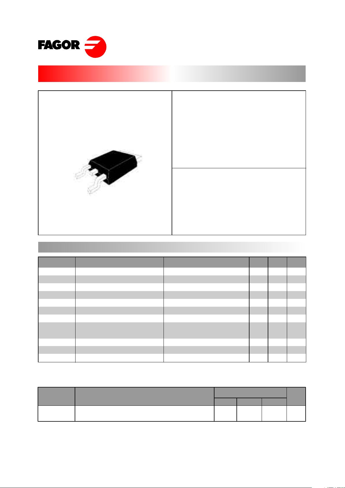
FT08...D
SURFACE MOUNT TRIAC
This series of TRIACs uses a high performance
PNPN technology.
These devices are intended for AC control
applications using surface mount technology.
The high commutation performances combined with
high sensitivity, make them perfect in all applications
like solid state relays, home appliances, power tools,
small motor drives...
Jun - 02
Absolute Maximum Ratings, according to IEC publication No. 134
RMS On-state Current
Non-repetitive On-State Current
Non-repetitive On-State Current
Fusing Current
Peak Gate Current
Peak Gate Dissipation
Gate Dissipation
Critical rate of rise of on-state current
Operating Temperature Range
Storage Temperature Range
Lead Temperature for soldering
I
T(RMS)
PARAMETER CONDITIONS Min. Max. Unit
DPAK
(Plastic)
Gate Trigger Current
< 5 mA to < 50 mA
Off-State Voltage
200 V ÷ 600 V
SYMBOL
I
TSM
I
TSM
I2t
I
GM
P
GM
P
G(AV)
T
j
T
stg
T
L
All Conduction Angle, TC = 110 ºC
Half Cycle, 60 Hz
Half Cycle, 50 Hz
t
p
= 10 ms, Half Cycle
20 µs max.
20 µs max.
20 ms max.
10s max.
8
84
80
36
50
-40
-40
A
A
A
A
2
s
A
W
W
A/µs
ºC
ºC
ºC
4
10
1
+125
+150
260
di/dt
MT1
MT2
G
MT2
Repetitive Peak Off State
Voltage
PARAMETER VOLTAGE UnitSYMBOL
V
DRM
V
RRM
B
200 V
M
600
D
400
Tr ≤ 100 ns, F = 120 Hz
T
j
= 125 ºC
I
G
= 2 x I
GT
Page 2

FT08...D
SURFACE MOUNT TRIAC
Jun - 02
PART NUMBER INFORMATION
FAGOR
SCR
CURRENT
CASE
VOLTAGE
SENSITIVITY
F T 08 08 B D 00
FORMING
TR
PACKAGING
Electrical Characteristics
Gate Trigger Current
Off-State Leakage Current
Threshold Voltage
Dynamic Resistance
On-state Voltage
Gate Trigger Voltage
Gate Non Trigger Voltage
Holding Current
Latching Current
Critical Rate of Voltage Rise
PARAMETER CONDITIONS SENSITIVITY
Unit
SYMBOL
I
GT
(1)
I
DRM
VD = 12 V
DC
, R
L
= 30Ω
mA
1
5
0.85
1.55
1.3
0.2
1.6
70
mA
mA
µA
V
mΩ
V
V
V
mA
mA
V/µs
A/ms
MAX
MAX
MAX
MAX
MAX
MAX
MAX
MIN
MAX
MAX
MAX
MIN
MIN
MIN
MIN
/I
RRM
V
TM
(2)
V
GT
V
GD
I
H
(2)
I
L
dv / dt
(2)
R
th(j-a)
Thermal Resistance
Junction-Ambient
Tj = 25 ºC
V
R
= V
RRM
,
IT = 11 Amp, tp = 380 µs, Tj = 25 ºC
VD = 12 V
DC
, R
L
= 30Ω, T
j
= 25 ºC
I
T
= 100 mA , Gate open, Tj = 25 ºC
I
G
= 1.2 IGT,
Tj
= 25 ºC
V
D
= 0.67 x V
DRM
, Gate open
T
j
= 125 ºC
Quadrant
Q1÷Q3
Q1÷Q3
Q1÷Q3
Q1,Q3
Q2
V
D
= V
DRM
, R
L
= 3.3KΩ, T
j
= 125 ºC
ºC/W
ºC/W
(1) Minimum IGT is guaranted at 5% of IGT max.
(2) For either polarity of electrode MT2 voltage with reference to electrode MT1.
R
th(j-c)
Thermal Resistance
Junction-Case
(dI/dt)c
(2)
Critical Rate of Current Rise
(dv/dt)c= 0.1 V/µs T
j
= 125 ºC
(dv/dt)c= 10 V/µs T
j
= 125 ºC
without snubber Tj = 125 ºC
V
to
(2)
R
d
(2)
Tj = 125 ºC
T
j
= 125 ºC
60
Tj = 125 ºC
Tj = 25 ºC
07
5
7
11
25
16
50
08
10
14
35
10
10
15
20
3.5
1.8
-
15
20
30
100
5.4
2.8
-
25
25
50
200
9
4.5
-
50
80
80
250
9
4.5
4.5
35
50
60
400
9
4.5
4.5
Page 3

10
8
6
4
2
0
Jun - 02
Fig. 1a: Maximum power dissipation versus
RMS on-state current (FT0807.D, FT0808.D).
0 25
50 75 100 125
P (W)
Fig. 2: Correlation between maximum power dissipation
and maximum allowable temperatures (Tamb and Tcase)
for different thermal resistances heatsink + contact.
T case (ºC)
-110
-115
-120
-125
Fig. 3: RMS on-state current versus ambient
temperature
Fig. 5: Relative variation of gate trigger current
and holding current versus junction temperature
(typical values).
IGT, IH (Tj) / IGT, IH (Tj = 25 ºC)
FT08...D
SURFACE MOUNT TRIAC
I
T(RMS)
(A)
0 2
10
8
6
4
2
0
4 6 8
P (W)
Tamb (ºC)
Tj (ºC)
Tamb (ºC)
I
T(RMS)
(A)
1 3 5 7
α = 90 º
α = 60 º
α = 30 º
9
8
7
6
5
4
3
2
1
0
0 25 50 75 100 125
-40 0
2.5
2.0
1.5
1.0
0.5
0.0
40 80 120-20 20 60 100
α
180 º
α
α = 180 º
α = 120 º
Fig. 1b: Maximum power dissipation versus
RMS on-state current (FT0811.D, FT0814.D).
0 2
10
8
6
4
2
0
4 6 8
P (W)
I
T(RMS)
(A)
1 3 5 7
α = 90 º
α = 60 º
α
180 º
α
α = 120 º
α = 180 º
α = 30 º
1.0
K = [Zth(j-c) / Rth (j-c)]
Fig. 4: Relative variation of thermal impedance
junction to case versus pulse duration.
1E-3 1E-2 1E-1 1E+0
tp (s)
0.5
0.2
0.1
Rth=15 ºC/W
Rth=10 ºC/W
Rth=5 ºC/W
Rth=0 ºC/W
α = 180 º
Rth(j-a) = Rth(j-c)
α = 180 º
Rth(j-a) = 55 ºC/W
S(Cu) = 1.75 cm
2
140
I
H
I
GT
Page 4

FT08...D
SURFACE MOUNT TRIAC
500
1 10
I
TSM
(A). I2t (A2s)
Fig. 7: Non repetitive surge peak on-state
current for a sinusoidal pulse with width:
tp < 10 ms, and corresponding value of I
2
t.
tp(ms)
2 5
Fig. 8: On-state characteristics (maximum
values).
1 10 100 1000
Fig. 6: Non repetitive surge peak on-state
current versus number of cycles.
80
70
60
50
40
30
20
10
0
I
TSM
(A)
Number of cycles
Fig. 9: Thermal resistance junction to ambient
versus copper surface under tab (Epoxy printed
circuit board FR4, copper thickness: 35 µm).
Tj initial = 25 ºC
F = 50 Hz
100
10
I2 t
I
TSM
Tj initial = 25 ºC
Jun - 02
0 0.5 1.0 1.5 2.0 2.5 3.0 3.5
ITM(A)
4.0
100.0
VTM(V)
4.5
10.0
1.0
0.1
5.0
Tj = Tj max.
Tj = 25 ºC
R
th(j-a)
(ºC/W)
S(Cu) (cm
2
)
0
100
80
60
40
20
0
2 4 6 8 10 12 14 16 18 20
Tj max
Vto = 0.8 V
Rd = 60 mΩ
Page 5

FT08...D
SURFACE MOUNT TRIAC
PACKAGE MECHANICAL DATA
DPAK TO 252-AA
A
A1
b
c
c1
c2
D
D1
E
E1
e
H
L
L1
L2
L3
L4
REF.
DIMENSIONS
Milimeters
Min. Nominal Max.
2.18
0
0.64
0.46
0.46
5.97
5.21
6.35
5.20
9.40
1.40
2.55
0.46
0.89
0.64
2.3±0.18
0.12
0.75±0.1
0.8±0.013
6.1±0.1
6.58±0.14
5.36±0.1
2.28BSC
9.90±0.15
2.6±0.05
0.5±0.013
1.20±0.05
0.83±0.1
2.39
0.127
0.89
0.61
0.56
6.22
5.52
6.73
5.46
10.41
1.78
2.74
0.58
1.27
1.02
Marking: type number
Weight: 0.2 g
8º
±2º
E
L3
D
be
4.57 Typ.
ø1x0.15
H
1.6
L4
A
c2
8º
±2º
8º
±2º
8º
±2º
8º
±2º
L
L2
A1
1.067
±0.013
E1
D1
Jun - 02
FOOT PRINT
6.7
6.7
3
1.6
2.32.3
1.6
3
 Loading...