

Page 1

On-State Current
4 Amp
FT04...H
LOGIC LEVEL TRIAC
This series of TRIACs uses a high
performance PNPN technology.
These par ts are intended for general
purpose AC switching applications with
highly inductive loads.
Dec - 02
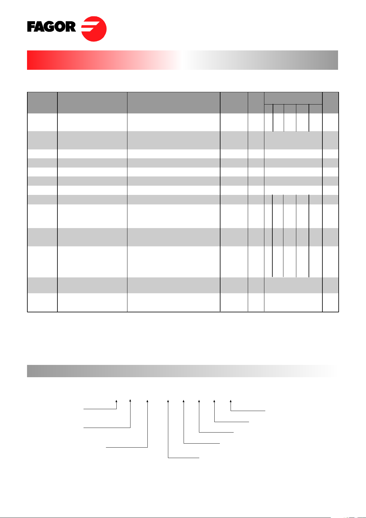
Absolute Maximum Ratings, according to IEC publication No. 134
TO220-AB
Gate Trigger Current
≤ 5 mA to ≤ 10 mA
Off-State Voltage
200 V ÷ 600 V
MT1
MT2
G
MT2
RMS On-state Current
Non-repetitive On-State Current
Non-repetitive On-State Current
Fusing Current
Peak Gate Current
Average Gate Power Dissipation
Critical rate of rise of on-state current
Operating Temperature
Storage Temperature
I
T(RMS)
PARAMETER CONDITIONS Min. Max. UnitSYMBOL
I
TSM
I2t
I
GM
P
G(AV)
T
j
T
stg
All Conduction Angle, TC = 110 ºC
Full Cycle, 60 Hz
Full Cycle, 50 Hz
t
p
= 10 ms, Half Cycle
20 µs max. T
j
=125ºC
T
j
=125ºC
I
G
= 2x IGT, t
r
≤100ns
f= 120 Hz, T
j
=125ºC
50
-40
-40
A
A
A
A
2
s
A
W
A/µs
ºC
ºC
4
33
30
4.5
4
1
+125
+150
di/dt
I
TSM
Repetitive Peak Off State
Voltage
PARAMETER VOLTAGE UnitSYMBOL
V
DRM
V
RRM
B
200 V
M
600
D
400
Page 2
FT04...H
LOGIC LEVEL TRIAC
Dec - 02
Electrical Characteristics
Gate Trigger Current
Off-State Leakage Current
Threshold Voltage
Dynamic Resistance
On-state Voltage
Gate Trigger Voltage
Gate Non Trigger Voltage
Holding Current
Latching Current
Critical Rate of Voltage Rise
PARAMETER CONDITIONS SENSITIVITY
Unit
SYMBOL
I
GT
(1)
I
DRM
VD = 12 V
DC
, R
L
= 33Ω, T
j
= 25 ºC
mA
1
5
0.9
120
1.6
1.3
0.2
2.6
60
mA
mA
µA
V
mΩ
V
V
V
mA
mA
V/µs
A/ms
MAX
MAX
MAX
MAX
MAX
MAX
MAX
MAX
MIN
MAX
MAX
MAX
MIN
MIN
MIN
MIN
/I
RRM
V
TM
(2)
V
GT
V
GD
I
H
(2)
I
L
dv / dt
(2)
R
th(j-a)
Thermal Resistance
Junction-Ambient
VD = V
DRM
,
T
j
= 25 ºC
V
R
= V
RRM
,
IT = 5.5 Amp, tp = 380 µs, Tj = 25 ºC
VD = 12 V
DC
, R
L
= 33Ω, T
j
= 25 ºC
I
T
= 100 mA , Gate open, Tj = 25 ºC
I
G
= 1.2 IGT,
Tj
= 25 ºC
V
D
= 0.67 x V
DRM
, Gate open
T
j
= 125 ºC
Quadrant
Q1÷Q3
Q4
Q1÷Q4
(3)
Q1÷Q4
(3)
Q1,Q3,Q4
(4)
Q2
V
D
= V
DRM
, R
L
= 3.3KΩ, T
j
= 125 ºC
ºC/W
ºC/W
09
10
10
15
25
30
40
2.7
2.0
-
(1) Minimum IGT is guaranted at 5% of IGT max.
(2) For either polarity of electrode MT2 voltage with reference to electrode MT1.
R
th(j-c)
Thermal Resistance
Junction-Case
(di/dt)c
(2)
Critical Rate of Current Rise
(dv/dt)c= 0.1 V/µs T
j
= 125 ºC
(dv/dt)c= 10 V/µs T
j
= 125 ºC
without snubber Tj = 125 ºC
V
to
(2)
R
d
(2)
Tj = 125 ºC
T
j
= 125 ºC
PART NUMBER INFORMATION
FAGOR
TRIAC
CURRENT
CASE
VOLTAGE
SENSITIVITY
F T 04 08 B H 00
FORMING
TU
PACKAGING
05
5
5
15
10
20
10
1.5
-
-
Tj = 125 ºC
07
5
7
08
10
10
10
15
20
1.8
0.9
-
20
20
40
20
2.5
-
-
04
5
15
10
20
10
1.5
-
-
(3) Q4 for 4 Quadrant Triacs
Q3 for 3 Quadrant Triacs
(4) Only for 4 Quadrant Triacs
Page 3

1 10 100 1000
30
25
20
15
10
5
0
I
TSM
(A)
Number of cycles
1E+0
1E-1
1E-2
K=[Zth / Rth]
1E-3 1E-2 1E-1 1E+0 1E+1 1E+2 5E+2
tp (s)
I
T(RMS)
(A)
Dec - 02
Fig. 1: Maximum power dissipation versus
RMS on-state curren (full cycle).
0 25 50 75 100 125
Fig. 2: RMS on-state current versus case
temperature (full cycle).
Fig. 3: : Relative variation of thermal
impedance versus pulse duration.
Fig. 5: Surge peak on-state current versus
number of cycles
Fig. 6: Non-repetitive surge peak on-state
current for a sinusoidal pulse with width
tp<10ms, and corresponding value of I
2
t.
Fig. 4: On-state characteristics (maximum
values)
FT04...H
LOGIC LEVEL TRIAC
P (W)
Tc (ºC)
I
T(RMS)
(A)
0 2 4
0
1
2
3
4
5
0
1.5
2.5
3.5
4.0
4.5
100
10
1
ITM (A)
0.5 1.0 1.5 2.0 2.5 3.0 5.0
VTM (V)
Zth(j-c)
Zth(j-a)
3.5 4.0 4.5
Tj max
Vto = 0.85 V
Rt = 35mΩ
0.01 0.10 1.00 10.00
100
I
TSM
(A), I2 t (A2s)
tp (ms)
Non repetitive
Tj initial = 25 ºC
Repetitive
Tc = 90 ºC
dl/dt limitation
50A/µs
1 3
0.5
1.0
2.0
3.0
Tj max
Tj = 25 ºC
t=20ms
One cycle
I2t
I
TSM
10
1
Tj initial = 25 ºC
Page 4

FT04...H
LOGIC LEVEL TRIAC
PACKAGE MECHANICAL DATA
TO-220AB (Plastic)
A
a1
a2
B
b1
b2
C
c1
c2
e
F
I
I4
L
I2
I3
M
REF.
DIMENSIONS
Milimeters
Min. Nominal Max.
15.20
13.00
10.00
0.61
1.23
4.40
0.49
2.40
2.40
6.20
3.75
15.80
2.65
1.14
1.14
3.75
16.40
2.60
15.90
14.00
10.40
0.88
1.32
4.60
0.70
2.72
2.70
6.60
3.85
16.80
2.95
1.70
1.70
14
a1
L
A
e
a2
b1
12
13
øI
B
c
F
b2
c2
c1
M
0
0.5
2.0
1.0
1.5
2.5
I
GT,IH,IL
[Tj]/I
GT,IH,IL
.[Tj=25ºC]
Fig. 7: Relative variation of gate trigger
current, holding current and latching versus
junction temperature (typical values)
Tj(ºC)
-40 -20 0 20 40 60 80 100120140
I
GT
IH&I
L
Dec - 02
0 25 50 75
Fig. 8: Relative variation of critical rate of
decrease of main current versus junction
temperature
(dI/dt)c [Tj]/(dI/dc)c [Tj specified]
100
6
5
4
3
2
1
0
Tj(ºC)
125
 Loading...