

Datasheet FST6800CW, FST6800WMX, FST6800WM, FST6800QSCX, FST6800QSC Datasheet (Fairchild Semiconductor)
...Page 1
© 1999 Fairchild Semiconductor Corporation DS500022 www.fairchildsemi.com
June 1997
Revised December 1999
FST6800 10-Bit Bus Switch with Pre-Charged Outputs
FST6800
10-Bit Bus Switch with Pre-Charged Outputs
General Description
The Fairchild Switch FST6800 provides 10-bits of highspeed CMOS TTL-comp atible bus switching. The low on
resistance of the switch allows inp uts to be connected to
outputs without adding propagation delay or generating
additional ground bounce noise. The device precharges
the B Port to a sele ctable b ias v oltage (BiasV) to minimi ze
live insertion noise.
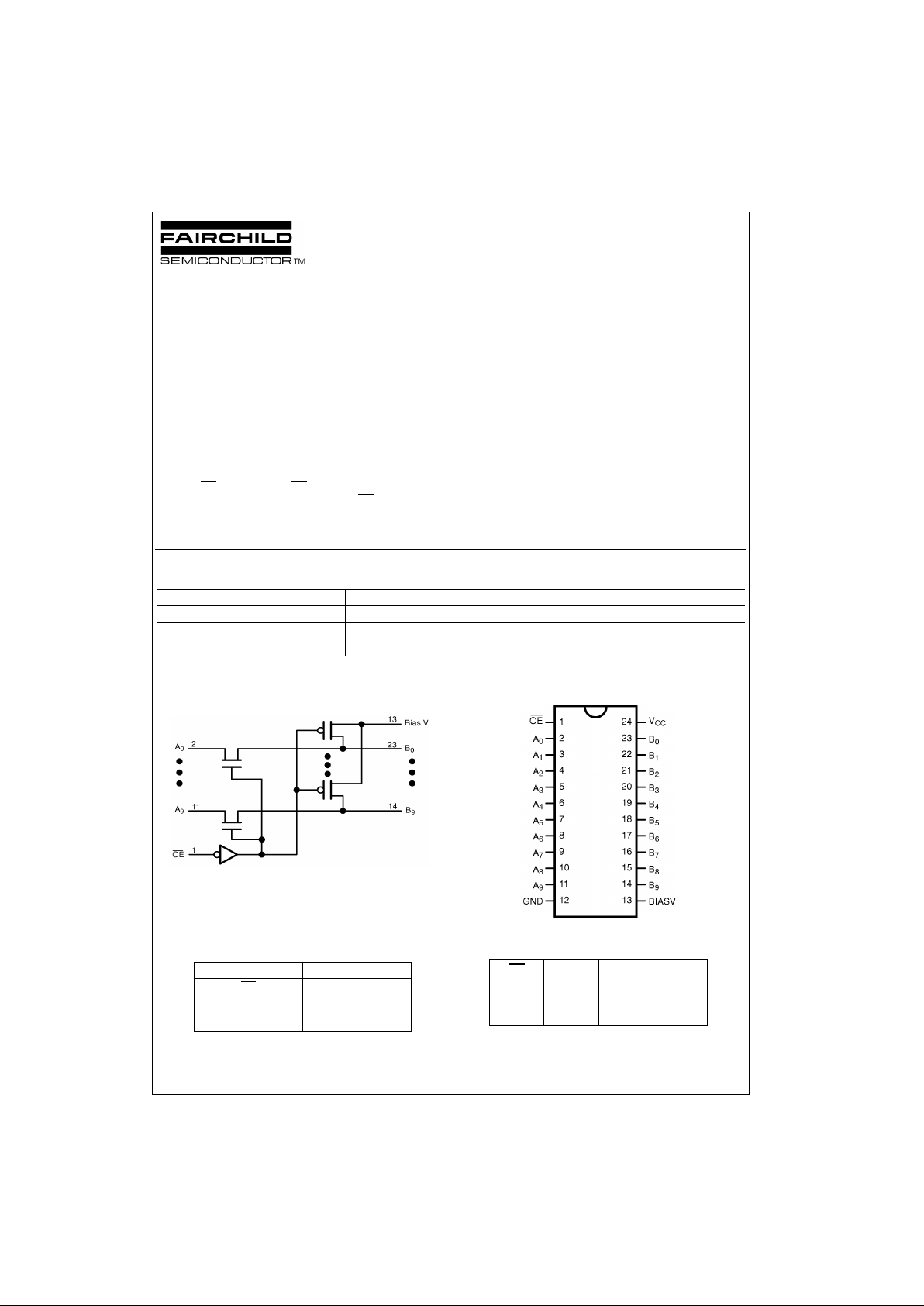
The device is organized as a 10-bit switch with a bus
enable (OE
) signal. When OE is LOW, the switch is ON
and Port A is connect ed to Po rt B. Whe n OE
is HIGH, the
switch is OPEN and the B Port is precharged to BiasV
through an equivalent 10-kΩ resistor.
Features
■ 4Ω switch connection between two ports.
■ Minimal propagation delay through the switch.
■ Low l
CC
.
■ Zero bounce in flow-through mode.
■ Output precharge to minimize live insertion noise.
■ Control inputs compatible with TTL level.
Ordering Code:
Devices also availab le in Tape and Reel. Specify by appending th e s uffix let t er “X” to the ordering code.
Logic Diagram
Pin Descriptions
Connection Diagram
Truth Table
Order Number Package Number Package Description
FST6800WM M24B 24-Lead Small Outline Integrated Circuit (SOIC), JEDEC MS-013, 0.300 Wide
FST6800QSC MQA24 24-Lead Quarter Size Outline Package (QSOP), JEDEC MO-137, 0.150 Wide
FST6800MTC MTC24 24-Lead Thin Shrink Small Outline Package (TSSOP), JEDEC MO-153, 4.4mm Wide
Pin Name Description
OE
Bus Switch Enable
ABus A
BBus B
OE B0–B
9
Function
LA
0–A9
Connect
HBiasV Precharge
Page 2
www.fairchildsemi.com 2
FST6800
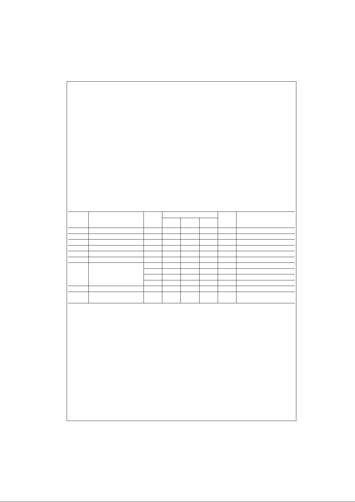
Absolute Maximum Ratings(Note 1) Recommended Operating
Conditions
(Note 3)
Note 1: The Absolute Maximum Ratings are those values beyond which
the safety of the dev ice cannot be guaranteed. T he device sh ould not be
operated at these limit s. The parametric values defin ed in the Electrical
Characteristics tables are not guaranteed at the absolute maximum ratings.
The Recommende d Opera ting Condit ions table s will de fine the co nditions
for actual device operation.
Note 2: The input and output ne gative vo ltage ra tings may be excee ded if
the input and output diode current ratings are observed.
Note 3: Unused control inputs must be held HIGH or LOW. They may not
float.
DC Electrical Characteristics
Note 4: Typi c al values are at VCC = 5.0V and TA= +25°C
Note 5: Measured by the volta ge drop between A and B pi ns at th e indicated current through the switch. On resistance is determined by the lower of the
voltages on the two (A or B) pins.
Supply Voltage (VCC) −0.5V to +7.0V
DC Switch Voltage (V
S
) −0.5V to +7.0V
Bias V Voltage Range −0.5V to +6.0V
DC Input Voltage (V
IN
) (Note 2) −0.5V to +7.0V
DC Input Diode Current (l
IK
) VIN<0V −50mA
DC Output (I
OUT
) Sink Current 128mA
DC V
CC
/GND Current (ICC/I
GND
) +/− 100mA
Storage Temperature Range (T
STG
) −65°C to +150 °C
Power Supply Operating (V
CC
) 4.0V to 5.5V
Precharge Supply (BiasV) 1.5V to V
CC
Input Voltage (VIN)0V to 5.5V
Output Voltage (V
OUT
)0V to 5.5V
Input Rise and Fall Time (t
r
, tf)
Switch Control Input 0nS/V to 5nS/V
Switch I/O 0nS/V to DC
Free Air Operating Temperature (T
A
) −40 °C to +85 °C
Symbol Parameter
V
CC
(V)
TA = −40 °C to +85 °C
Units Conditions
Min
Typ
(Note 4)
Max
V
IK
Clamp Diode Voltage 4.5 −1.2 V IIN = −18mA
V
IH
HIGH Level Input Voltage 4.0–5.5 2.0 V
V
IL
LOW Level Input Voltage 4.0–5.5 0.8 V
I
I
Input Leakage Current 5.5 ±1.0 µA0≤ VIN ≤5.5V
I
O
Output Current 4.5 0.25 mA BiasV = 2.4V, B = 0
I
OZ
OFF-STATE Leakage Current 5.5 ±1.0 µA0 ≤A ≤V
CC
R
ON
Switch On Resistance 4.5 4 7 Ω VIN = 0V, IIN = 64mA
(Note 5) 4.5 4 7 Ω V
IN
= 0V, IIN = 30mA
4.5 8 15 Ω V
IN
= 2.4V, IIN = 15mA
4.0 11 20 Ω VIN = 2.4V, IIN = 15mA
I
CC
Quiescent Supply Current 5.5 3 µAVIN = VCC or GND, I
OUT
= 0
∆ I
CC
Increase in I
CC
per Input 5.5 2.5 mA One input at 3.4V
Other inputs at VCC or GND
Page 3

3 www.fairchildsemi.com
FST6800
AC Electrical Characteristics
Note 6: This par ameter is guaranteed by design but is not test ed. The bus swit c h c ontributes no propagation delay other than the RC delay of the typical On
resistance of the switch and the 50pF load capacitance, when driven by an ideal voltage the source (zero output impedance).
Capacitance (Note 7)
Note 7: TA = +25°C, f = 1 MHz, Ca pacitance is characteriz ed but not tested.
AC Loading and Waveforms
Note: Input driven by 50 Ω source terminated in 50 Ω
Note: C
L
includes load and stray capacitance
Note: Input PRR = 1.0 MHz, t
W
= 500 ns
FIGURE 1. AC Test Circuit
FIGURE 2. AC Waveforms
Symbol Parameter
T
A
= −40 °C to +85 °C,
C
L
= 50pF, RU = RD = 500Ω
Units Conditions Figure No.
V
CC
= 4.5 – 5.5V VCC = 4.0V
Min Max Min Max
t
PHL,tPLH
Prop Delay Bus to Bus (Note 6) 0.25 0.25 ns VI = OPEN Figures 1,
2
t
PZH
Output Enable Time 1.5 6.2 6.5 ns VI = OPEN, BiasV = GND
Figure 1
Figure 2
t
PZL
1.5 6.2 6.5 ns VI = 7V, BiasV = 3V
t
PHZ
Output Disable Time 1.5 6.1 6.5 ns VI = OPEN, BiasV = GND
Figure 1
Figure 2
t
PLZ
1.5 7.3 6.8 ns VI = 7V, BiasV = 3V
Symbol Parameter Typ Max Units Conditions
C
IN
Control Pin Input Capacitance 3 pF VCC = 5.0V
C
I/O
Input/Output Capacitance 5 pF VCC, OE = 5.0V
Page 4

www.fairchildsemi.com 4
FST6800
Physical Dimensions inches (millimeters) unless otherwise noted
24-Lead Small Outline Integrated Circuit (SOIC), JEDEC MS-013, 0.300 Wide
Package Number M24B
24-Lead Quarter Size Outline Package (QSOP), JEDEC MO-137, 0.150 Wide
Package Number MQA24
Page 5

5 www.fairchildsemi.com
FST6800 10-Bit Bus Switch with Pre-Charged Outputs
Physical Dimensions inches (millimeters) unless otherwise noted (Continued)
24-Lead Thin Shrink Sm all Ou tline Pa ck age (TS SO P), JE DE C MO-153, 4.4mm Wide
Package Number MTC24
Technology Description
The Fairchild Switch family derives from and embodies Fairchild’s proven switch t echnology used for several years in it s
74LVX3L384 (FST3384) bus switch product.
Fairchild does not assume any responsibility for use of any circuitry described , no circuit patent licenses are implied and
Fairchild reserves the right at any time without notice to change said circuitry and specifications.
LIFE SUPPORT POLICY
FAIRCHILD’S PRODUCTS ARE NOT AUTHORIZED FOR USE AS CRITICAL COMPONENTS IN LIFE SUPPORT
DEVICES OR SYSTEMS WITHOUT THE EXPRESS WRITTEN APPROVAL OF THE PRESIDENT OF FAIRCHILD
SEMICONDUCTOR CORPORATION. As used herein:
1. Life support devices or systems are dev ices or syste ms
which, (a) are intended for surgical implant into the
body, or (b) support or sustain life, and (c) whose failure
to perform when properly used in accordance with
instructions for use provide d in the labe l ing, can be re asonably expected to result in a significant injury to the
user.
2. A critical component i n any compo nent o f a l ife supp ort
device or system whose failure to perform can be reasonably expected to cause the failure of the l ife support
device or system, or to affect its safety or effectiveness.
www.fairchildsemi.com
 Loading...