

Datasheet FST3383WMX, FST3383WM, FST3383QSCX, FST3383QSC, FST3383MTCX Datasheet (Fairchild Semiconductor)
...Page 1

December 1993
Revised May 1999
FST3383 10-Bit Low Power Bus-Exchange Switch
© 1999 Fairchild Semiconductor Corporation DS011652.prf www.fairchildsemi.com
FST3383
10-Bit Low Power Bus-Exchange Switch
General Description
The FST3383 provides two sets of high-speed CMOS TTLcompatible bus switches. The low on resistance of the
switch allows inputs to be connected to outputs without
adding propagation de lay or generating additi onal ground
bounce noise. The device operates as a 10 -bit bus switch
or a 5-bit bus exchange r. The bus exchange (BX ) signal
provides nibble swapping of the AB and CD pairs of signals. This exchange configur ation allows b yte swappin g of
buses in systems. It can also b e used as a quad 2-to-1
multiplexer and to creat e l ow del a y ba rr el shi f ter s. T he b us
enable (BE
) signal turns the switches ON.
Features
■ 5Ω switch connection between two ports
■ Zero propagation delay
■ Ultra low power with 0.2 µA typical I
CC
■ Zero ground bounce in flow-through mode
■ Control inputs compatible with TTL level
Ordering Code:
Devices also availab le in Tape and Reel. Specify by appending th e s uffix let t er “X” to the ordering cod e.
Logic Diagram
Pin Descriptions
Connection Diagram
Truth Table
Order Number Package Number Package Description
FST3383WM M24B 24-Lead Small Outline Integrated Circuit (SOIC), JEDEC MS-013, 0.300 Wide
FST3383QSC MQA24 24-Lead Quarter Size Outline Package (QSOP), JEDEC MO-137, 0.150 Wide
FST3383MTC MTC24 24-Lead Thin Shrink Small Outline Package (TSSOP), JEDEC MO-153, 4.4mm Wide
Pin Names Description
BE
Bus Switch Enable
BX Bus Exchange
A
0–A4
, B0–B
4
Buses A, B
C
0–C4
, D0–D
4
Buses C, D
BE BX
A
0–A4
B0–B
4
Function
H X High-Z State High-Z State Disconnect
LLC
0–C4
D0– D
4
Connect
LHD
0–D4
C0–C
4
Exchange
Page 2
www.fairchildsemi.com 2
FST3383
Absolute Maximum Ratings(Note 1) Recommended Operating
Conditions
Note 1: The “Absolute Maximum Ratin gs” are those v alues beyon d which
the safety of the dev ice cannot be guaranteed. T he device sh ould not be
operated at these limits. The parametric values defined in the Electrical
Characteristics tables are not guaranteed at the absolute maximum ratings.
The “Recommend ed O peratin g Cond itions” t able w ill defin e the co ndition s
for actual device operation.
Note 2: The input and output negative volt age ratin gs may be exceede d if
the input and output diode current ratings are observed.
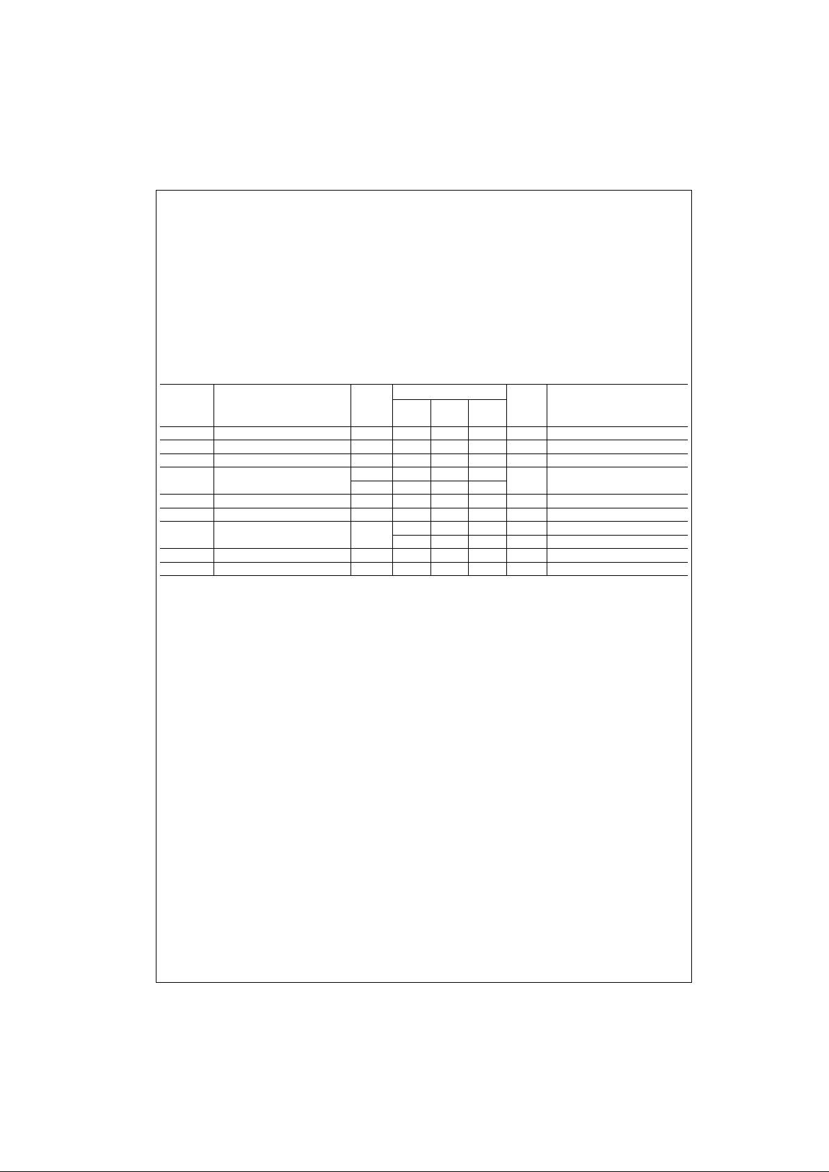
DC Electrical Characteristics
Note 3: All typical va lues are at VCC = 5.0V, TA = 25°C.
Note 4: Measured by v oltage drop between A and B pin at indicated current through the switch. On resistanc e is determined by the lower of the voltages on
the two (A or B) pins.
Note 5: Per TTL driven input (VIN = 3.15V, control inputs only). A and B pins do not contribute t o ICC.
Supply Voltage (VCC) −0.5V to +7.0V
DC Switch Voltage (V
S
) −0.5V to +7.0V
DC Input Voltage (V
I
) (Note 2) −0.5V to +7.0V
DC Input Diode Current (I
IN
)
with V
I
< 0
−20 mA
DC Output (I
O
) Sink Current 120 mA
Storage Temperature Range (T
STG
) −65°C to +150°C
Power Dissipation 0.5W
Supply Voltage (V
CC
) 4.0V to 5.5V
Free Air Operating Temperature (T
A
) −40°C to +85°C
Symbol Parameter
V
CC
(V)
TA = −40°C to +85°C
Units Conditions
Min Typ Max
(Note 3)
V
IK
Maximum Clamp Diode Voltage 4.75 −1.2 V IIN = −18 mA
V
IH
Minimum High Level Input Voltage 4.75–5.25 2.0 V
V
IL
Maximum Low Level Input Voltage 4.75–5.25 0.8 V
I
IN
Maximum Input 0 10 µA0 ≤ VIN ≤ 5.25V
Leakage Current 5.25 ±1
I
OZ
Maximum 3-STATE I/O Leakage 5.25 ±10 µA0 ≤ A, B ≤ V
CC
I
OS
Short Circuit Current 4.75 100 mA VI(A), VI(B) = 0V, VI(B), VI(A) = 4.75V
R
ON
Switch On Resistance (Note 4) 4.75 5 7 Ω VI = 0V, ION = 30 mA
10 15 Ω VI = 2.4V, ION = 15 mA
I
CC
Maximum Quiescent Supply Current 5.25 0.2 10 µAVI = VCC, GND, IO = 0
∆I
CC
Increase in ICC per Input (Note 5) 5.25 2.5 mA VIN = 3.15V, IO = 0, Per Control Input
Page 3

3 www.fairchildsemi.com
FST3383
AC Electrical Characteristics
Note 6: All typical value s are at VCC = 5.0V, TA = 25°C.
Note 7: This paramet er is gua rantee d by desig n but not tested . The bus switch c ontribu tes no pro pagatio n dela y other th an the RC delay of the On resis-
tance of the switch and the load capacitance. The time constant for the switch and alone is of the order of 0.25 ns for 50 pF load. Since this time constant is
much smaller than the rise /fal l time s of typic al d riving sig na ls, it adds ve ry litt le pro pa gati on de lay t o t he s yste m. Pro pa gation delay of the bus switch when
used in a system is determined by the driving circuit on the driving side of the switch and its interaction with the load on the driven side.
Capacitance (Note 8)
Note 8: Capacitance is ch aracterized but not tes te d.
On-Resistance (R
ON
) vs Input Voltage
(V
CC
= 5.0V)
Symbol Parameter
V
CC
(V)
TA = −40°C to +85°C, CL = 50 pF
Units
Min Typ Max
(Note 6)
t
PLH
, Data Propagation Delay 4.75 0.25 ns
t
PHL
An to Cn, Dn or Bn to Dn, Cn (Note 7)
t
PLH
, Switch Exchange Time 4.75 1.5 6.5 ns
t
PHL
BX to An, Bn, Cn, D
n
t
PZL
, Switch Enable Time 4.75 1.5 6.5 ns
t
PZH
BE to An, Bn, Cn or D
n
t
PLZ
, Switch Disable Time 4.75 1.5 5.5 ns
t
PHZ
BE to An, Bn, Cn, or D
n
Symbol Parameter Typ Max Units Conditions
C
IN
Control Input Capacitance 4 6 pF VCC = 5.0V
C
I/O
(OFF) Input/Output Capacitance 9 13 pF VCC = 5.0V
Page 4

www.fairchildsemi.com 4
FST3383
Physical Dimensions inches (millimeters) unless otherwise noted
24-Lead Small Outline Integrated Circuit (SOIC), JEDEC MS-013, 0.300 Wide
Package Number M24B
24-Lead Quarter Size Outline Package (QSOP), JEDEC MO-137, 0.150 Wide
Package Number MQA24
Page 5

Fairchild does not assume any responsibility for use of any circuitry described, no circuit patent licenses are implied and Fairchild reserves the right at any time without notice to change said circuitry and specifications.
FST3383 10-Bit Low Power Bus-Exchange Switch
LIFE SUPPORT POLICY
FAIRCHILD’S PRODUCTS ARE NOT AUTHORIZED FOR USE AS CRITICAL COMPONENTS IN LIFE SUPPORT
DEVICES OR SYSTEMS WITHOUT THE EXPRESS WRITTEN APPROVAL OF THE PRESIDENT OF FAIRCHILD
SEMICONDUCTOR CORPORATION. As used herein:
1. Life support devices or systems are dev ices or syste ms
which, (a) are intended for surgical implant into the
body, or (b) support or sustain life, and (c) whose failure
to perform when properly used in accordance with
instructions for use provided i n the labe li ng, can be re asonably expected to result in a significant injury to the
user.
2. A critical component in any com ponen t of a life s uppor t
device or system whose failu re to perform can b e reasonably expected to c ause th e fa i lure of the li fe s upp or t
device or system, or to affect its safety or effectiveness.
www.fairchildsemi.com
Physical Dimensions inches (millimeters) unless otherwise noted (Continued)
24-Lead Thin Shrink Small Outline Package (TSSOP), JEDEC MO-153, 4.4mm Wide
Package Number MTC24
Technology Description
The Fairchild Switch family derives from a nd embodies Fair child’s proven switch technolo gy used for severa l years in its
74LVX3L384 (FST3384) bus switch product.
 Loading...