

Page 1
查询FST3244供应商
FST3244
Octal Bus Switch
FST3244 Octal Bus Switch
June 1997
Revised December 1999
General Description
The Fairchild Switch FST3244 provides 8-bits of highspeed CMOS TTL-comp atible bus switch ing in a standa rd
’244 pin-out. The low on res istance of the switch allows
inputs to be connect ed to output s with out ad ding prop agation delay or generating additional ground bounce noise.
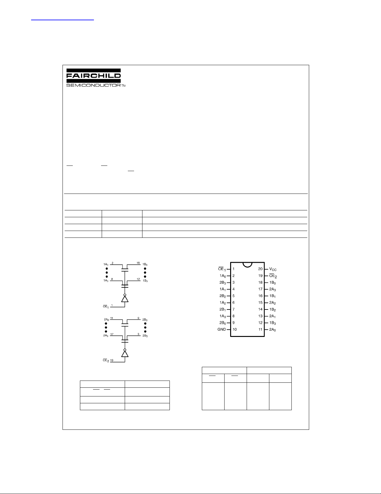
The device is organized as two 4-bit switches with separate
inputs. When OE is LOW, the switch is ON and Port A
OE
is connected to P ort B. When OE
OPEN and a high- impe dan ce state exists betwe en th e tw o
ports.
is HIGH, the switch is
Features
■ 4Ω switch connection between two ports.
■ Minimal propagation delay through the switch.
■ Low l
■ Zero bounce in flow-through mode.
■ Control inputs compatible with TTL level.
.
CC
Ordering Code:
Order Number Package Number Package Description
FST3244WM M20B 20-Lead Small Outline Integrated Circuit (SOIC), JEDEC MS-013, 0.300 Wide
FST3244QSC MQA20 20-Lead Quarter Size Outline Package (QSOP), JEDEC MO-137, 0.150 Wide
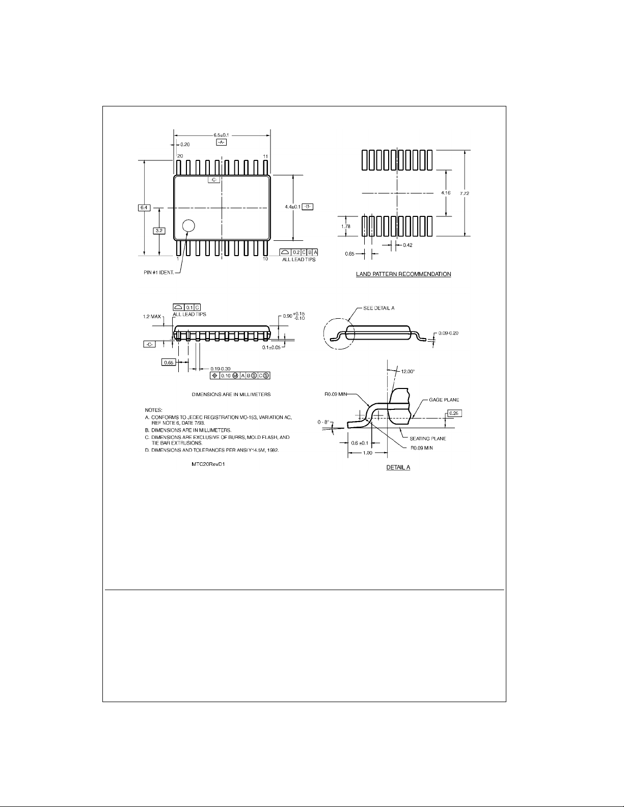
FST3244MTC MTC20 20-Lead Thin Shrink Small Outline Package (TSSOP), JEDEC MO-153, 4.4mm Wide
Devices also availab le in Tape and Reel. Specify by appending th e s uffix let t er “X” to the ordering cod e.
Logic Diagram
Connection Diagram
Truth T able
Pin Descriptions
Pin Name Description
, OE
OE
1
2
1A, 2A Bus A
1B, 2B Bus B
© 1999 Fairchild Semiconductor Corporation DS500021 www.fairchildsemi.com
Bus Switch Enable
Inputs Inputs/Outputs
OE
LL1A = 1B 2A = 2B
LH1A = 1B Z
HLZ2A = 2B
HHZZ
OE
1
1A, 1B 2A, 2B
2
Page 2
Absolute Maximum Ratings(Note 1) Recommended Operating
Supply Voltage (VCC) −0.5V to +7.0V
DC Switch Voltage (V
FST3244
DC Input Voltage (V
DC Input Diode Current (l
DC Output (I
DC V
OUT
/GND Current (ICC/I
CC
Storage Temperature Range (T
) −0.5V to +7.0V
S
) (Note 2) −0.5V to +7.0V
IN
) VIN<0V −50mA
IK
) Sink Current 128mA
) +/− 100mA
GND
) −65°C to +150 °C
STG
Conditions
Power Supply Operating (V
Input Voltage (V
Output Voltage (V
Input Rise and Fall Time (t
Switch Control Input 0nS/V to 5nS/V
Switch I/O 0nS/V to DC
Free Air Operating Temperature (T
Note 1: The Absolute Maximum Ratings are those values beyond which
the safety of the dev ice cannot be guaranteed. T he device sh ould not be
operated at these limits. The parametric values defined in the Electrical
Characteristics tables are not guaranteed at the absolute maximum rating.
The Recommende d Opera ting Condit ions table s will de fine the co nditions
for actual device operation.
Note 2: The input and output negative volt age ratin gs may be exceede d if
the input and output diode current ratings are observed.
Note 3: Unused control inputs must be held HIGH o r LOW. They may no t
float.
(Note 3)
) 4.0V to 5.5V
CC
)0V to 5.5V
IN
)0V to 5.5V
OUT
, tf)
r
) −40 °C to +85 °C
A
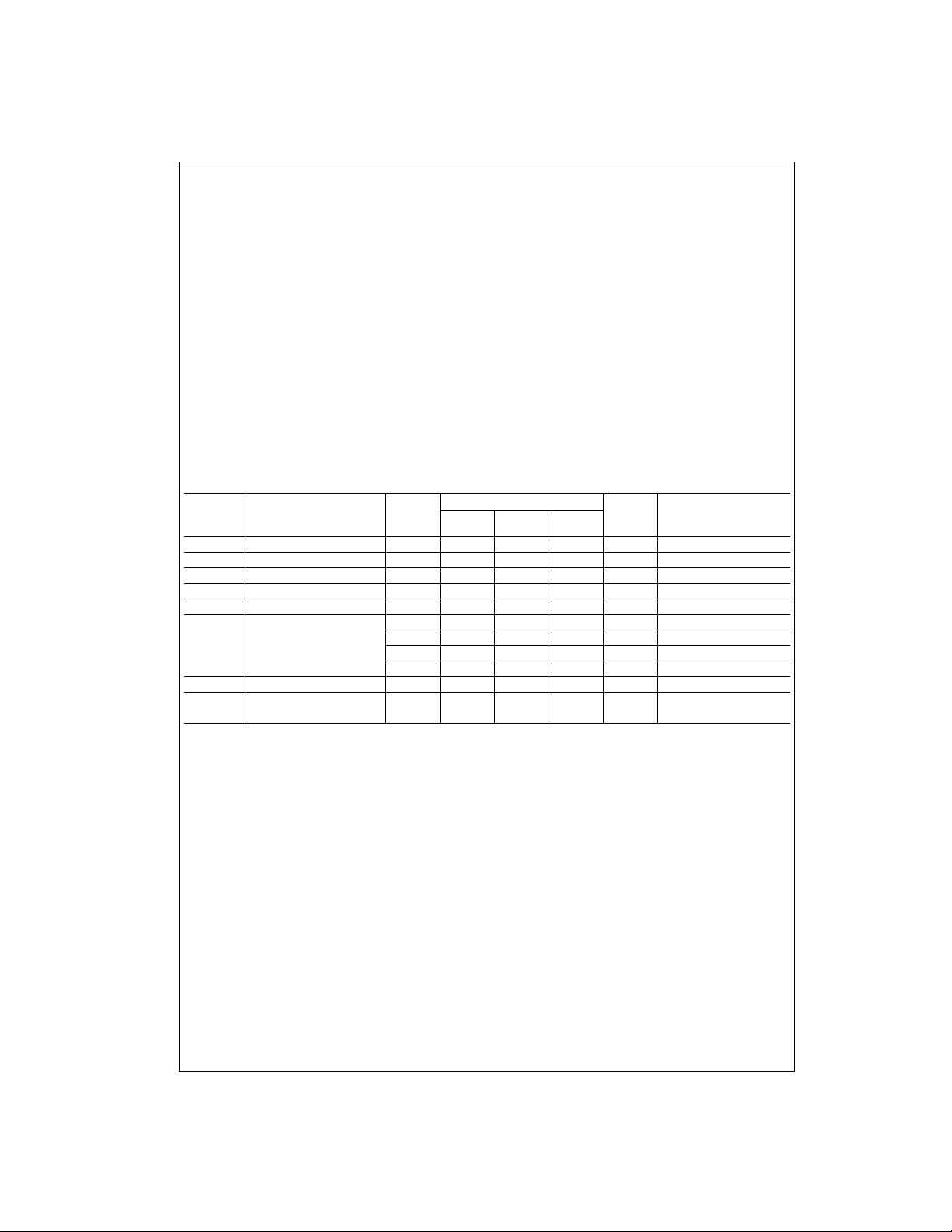
DC Electrical Characteristics
V
Symbol Parameter
V
IK
V
IH
V
IL
I
I
I
OZ
R
ON
I
CC
∆ I
CC
Note 4: Typical values are at VCC = 5.0V and TA = +25°C
Note 5: Measured by th e v olt age drop between A and B pins at the indicate d c urrent through the switch. On resistance is det erm ined by the lower of the
voltages on the two (A or B) pins.
Clamp Diode Voltage 4.5 −1.2 V IIN = −18mA
High Level Input Voltage 4.0–5.5 2.0 V
Low Level Input Voltage 4.0–5.5 0.8 V
Input Leakage Current 5.5 ±1.0 µA0≤ VIN ≤5.5V
OFF-STATE Leakage Current 5.5 ±1.0 µA0 ≤A, B ≤V
Switch On Resistance 4.5 4 7 Ω VIN = 0V, IIN = 64mA
(Note 5) 4.5 4 7 Ω VIN = 0V, IIN = 30mA
Quiescent Supply Current 5.5 3 µAVIN = VCC or GND, I
Increase in I
per Input 5.5 2.5 mA One input at 3.4V
CC
CC
(V)
4.5 8 15 Ω VIN = 2.4V, IIN = 15mA
4.0 11 20 Ω VIN = 2.4V, IIN = 15mA
TA = −40 °C to +85 °C
Min
Typ
(Note 4)
Max
Units Conditions
CC
Other inputs at VCC or GND
OUT
= 0
www.fairchildsemi.com 2
Page 3
AC Electrical Characteristics
TA = −40 °C to +85 °C,
Symbol Parameter
t
PHL,tPLH
t
PZH
t
PHZ
Note 6: This parameter is guaranteed by design but is not test ed. The bus switch contrib ut es no propagation delay oth er th an the RC delay of the typical On
resistance of the switc h and the 50pF load cap ac it ance, when driven by a n ideal voltage the source (z ero output impedan ce ).
Prop Delay Bus to Bus(Note 6) 0.25 0.25 ns VI = OPEN Figure 1
, t
Output Enable Time 1.0 5.6 6.1 ns VI = 7V for t
PZL
, t
Output Disable Time 1.0 6.2 5.6 ns VI = 7V for t
PLZ
CL = 50pF, RU = RD = 500Ω
VCC = 4.5 – 5.5V VCC = 4.0V
Min Max Min Max
Units Conditions Figure No.
Figure 2
PZL Figure 1
VI = OPEN for t
VI = OPEN for t
Figure 2
PZH
PLZ Figure 1
Figure 2
PHZ
Capacitance (Note 7)
Symbol Parameter Typ Max Units Conditions
C
IN
C
I/O
Note 7: TA = +25°C, f = 1 MHz, Capacitance is characterized but not tested.
Control Pin Input Capacitance 3 pF VCC = 5.0V
Input/Output Capacitance 5 pF VCC, OE = 5.0V
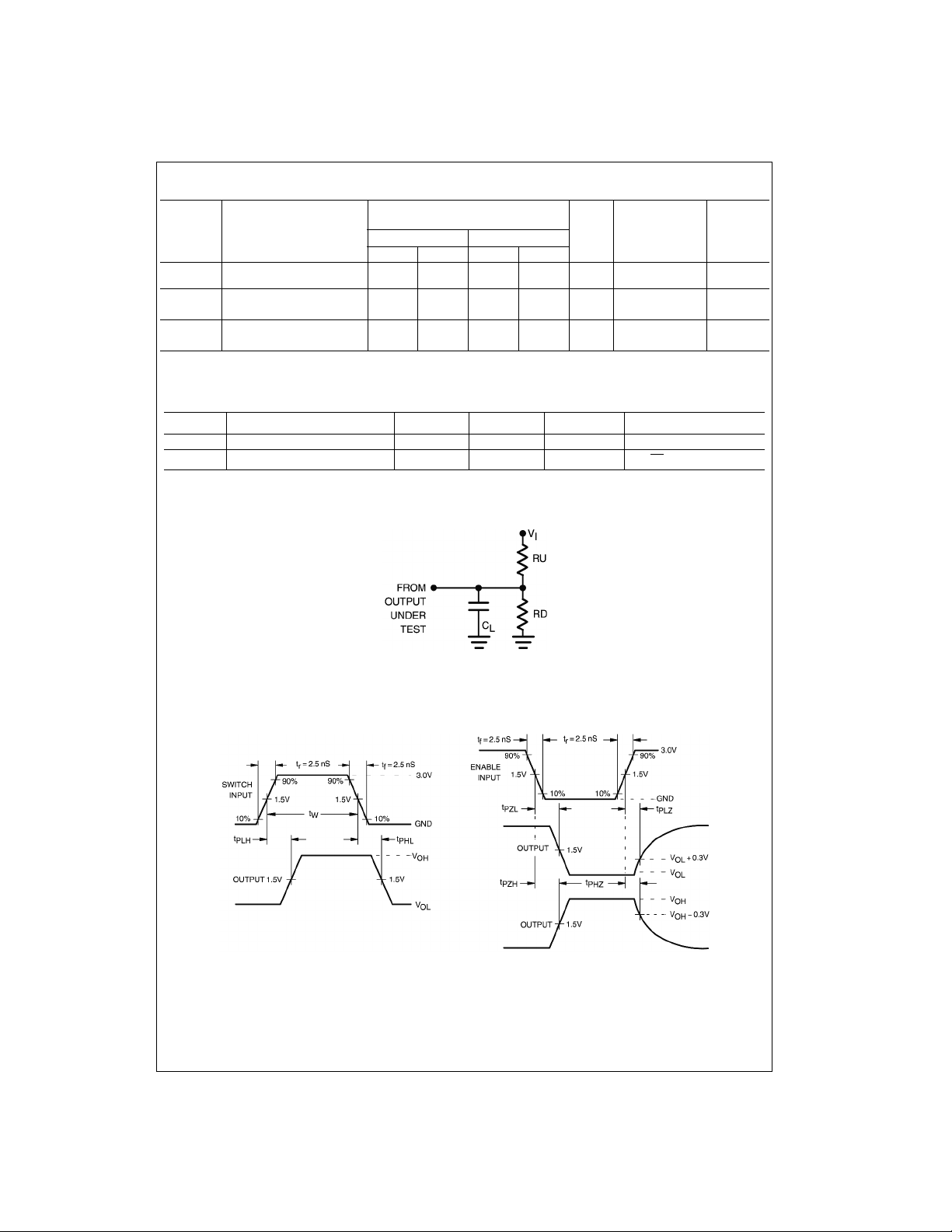
AC Loading and Waveforms
FST3244
Note: Input driven by 50 Ω source terminated in 50 Ω
includes load and stray capacitance
Note: C
L
Note: Input PRR = 1.0 MHz, t
= 500 nS
W
FIGURE 1. AC Test Circuit
FIGURE 2. AC Waveforms
3 www.fairchildsemi.com
Page 4
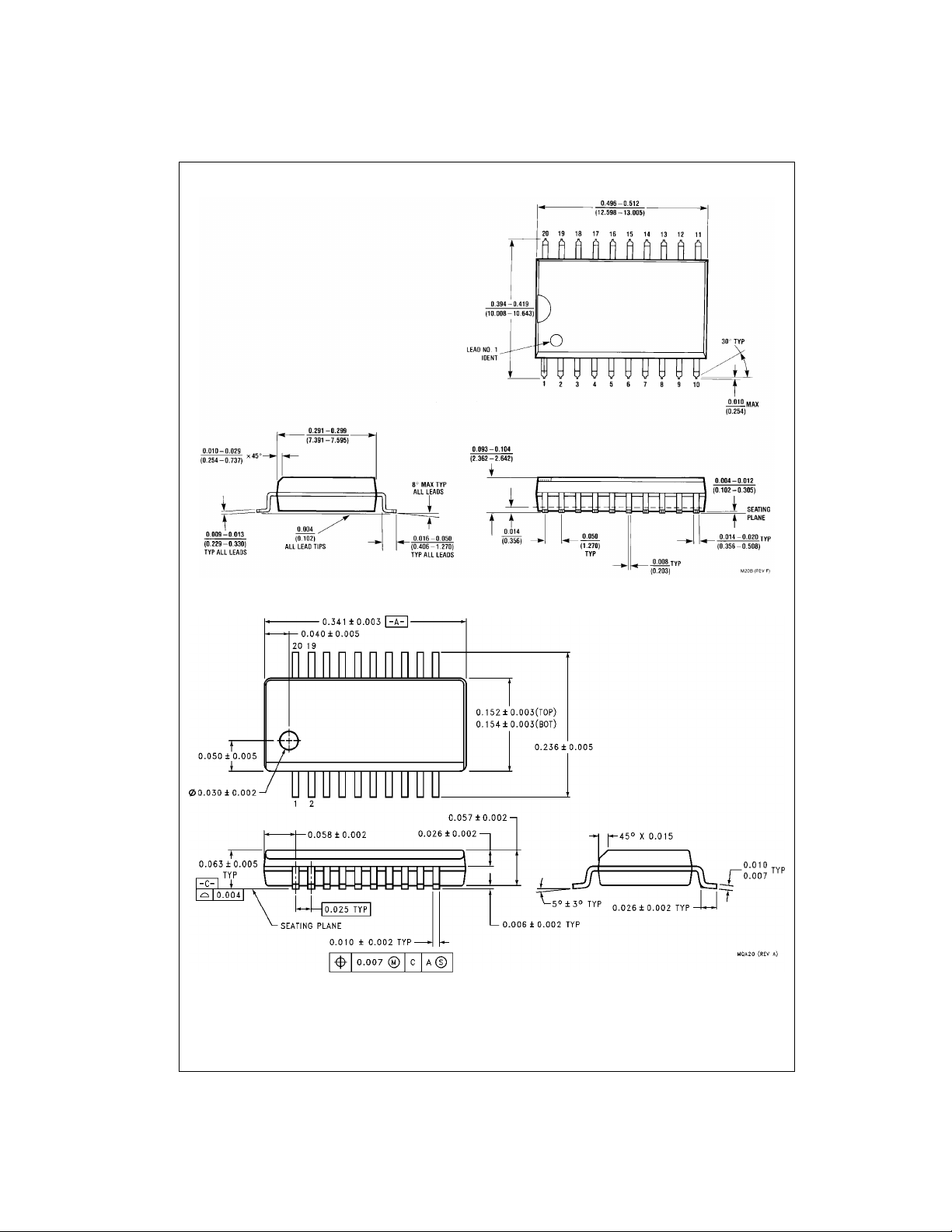
Physical Dimensions inches (millimeters) unless otherwise noted
FST3244
20-Lead Small Outline Integrated Circuit (SOIC), JEDEC MS-013, 0.300 Wide
20-Lead Quarter Size Outline Package (QSOP), JEDEC MO-137, 0.150 Wide
Package Number M20B
Package Number MQA20
www.fairchildsemi.com 4
Page 5
Physical Dimensions inches (millimeters) unless otherwise noted (Continued)
FST3244 Octal Bus Switch
20-Lead Thin Shrink Small Outline Package (TSSOP), JEDEC MO-153, 4.4mm Wide
Package Number MTC20
Technology Description
The Fairchild Switch family derives fro m and embodies Fair child’s proven switch technolo gy used for severa l years in its
74LVX3L384 (FST3384) bus switch product.
Fairchild does not assume any responsibility for use of any circuitry described, no circuit patent license s are implied and
Fairchild reserves the right at any time without notice to change said circuitry and specifications.
LIFE SUPPORT POLICY
FAIRCHILD’S PRODUCTS ARE NOT AUTHORIZED FOR USE AS CRITICAL COMPONENTS IN LIFE SUPPORT
DEVICES OR SYSTEMS WITHOUT THE EXPRESS WRITTEN APPROVAL OF THE PRESIDENT OF FAIRCHILD
SEMICONDUCTOR CORPORATION. As used herein:
1. Life support devices or systems are devices or systems
which, (a) are intended for surgical implant into the
body, or (b) support or sustain life, and (c) whose failure
to perform when properly used in accordance with
instructions for use provide d in the labe l ing, can be re asonably expected to result in a significant injury to the
user.
2. A critical componen t in any com ponen t of a life s upport
device or system whose failu re to perform can b e reasonably expected to cause the failure of the life support
device or system, or to affect its safety or effectiveness.
www.fairchildsemi.com
5 www.fairchildsemi.com
 Loading...