

Page 1
FST162244
Preliminary
FST162244 16-Bit Bus Switch with 25
May 2001
Revised May 2001
16-Bit Bus Switch with 25
Ω Series Resistor in Outputs
(Preliminary)
General Description
The Fairchild Switch FST162244 provid es 16-bits of hig hspeed CMOS TTL-compatible bus switching. The low On
Resistance of the switch allows inputs to be connected to
outputs without adding propagation delay or generating
additional ground bounce noise.
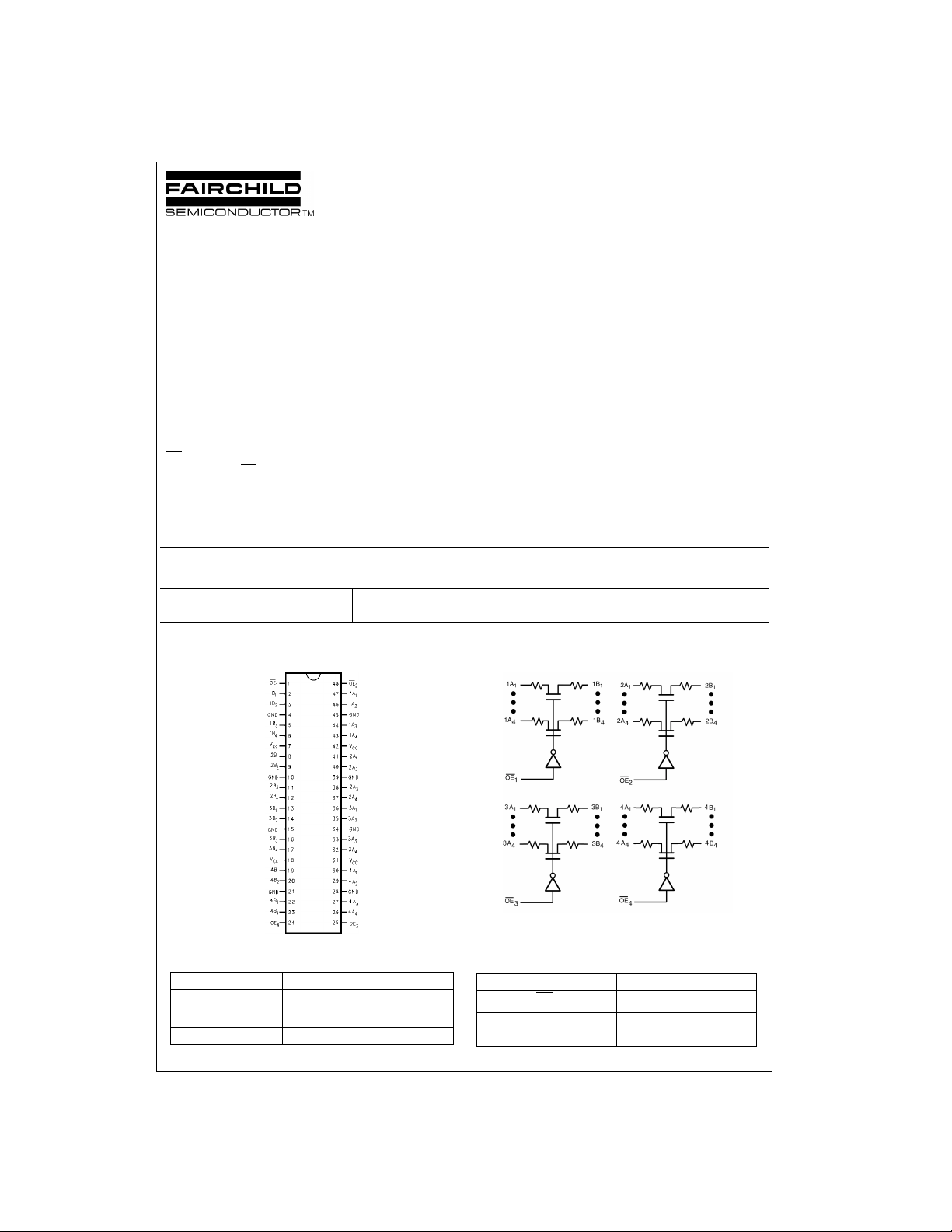
The device is o rganized a s a 16- bit switch . There are fo ur
4-bit switches with separ ate output enable inputs. When
OE
is LOW, the switch in ON and P ort A is connected to
Port B. When OE
impedance state exi sts between the A and B Po rts. The
FST162244 has an equivalent 25
reduce signal-reflection noise, eliminating the need for
external terminating resistors.
is HIGH, the switch OFF and a high
Ω series resistors to
Ordering Code:
Order Number Package Number Package Description
FST162244MTD MTD48 48-Lead Thin Shrink Small Outline Package (TSSOP), JEDEC MO-153, 6.1mm Wide
Devices also availab le in Tape and Reel. Specify by appending the suffix letter “X” to the o rdering code.
Connection Diagram
Features
■ 25Ω switch connection between two ports.
■ Minimal propagation delay through the switch.
■ Low l
■ Zero bounce in flow-through mode.
■ Control inputs compatible with TTL level.
.
CC
Logic Diagram
Ω
Series Resistor in Outputs (Preliminary)
Pin Descriptions
Pin Name Description
OE
n
, 2An, 3An, 4A
1A
n
1B
, 2Bn, 3Bn, 4B
n
© 2001 Fairchild Semiconductor Corporation DS500430 www.fairchildsemi.com
Output Enable Input (Active LOW)
n
n
Bus A
Bus B
Truth Table
Inputs Outputs
OE
x
LA Port
H = HIGH Voltage Level L = LOW Voltage Level Z = High Impedance
HZ
A, B
= B Port
Page 2
Preliminary
Absolute Maximum Ratings(Note 1) Recommended Operating
Supply Voltage (VCC) −0.5V to +7.0V
DC Switch Voltage (V
DC Input Voltage (V
FST162244
DC Input Diode Current (l
DC Output Current (I
DC V
/GND Current (ICC/I
CC
Storage Temperature Range (T
) (Note 2) −0.5V to +7.0V
S
) (Note 3) −0.5V to +7.0V
IN
) V
< 0V −50 mA
IK
IN
) 128 mA
OUT
) ±100 mA
GND
) −65°C to +150 °C
STG
Conditions
Power Supply Operating (V
Input Voltage (V
Output Voltage (V
Input Rise and Fall Time (t
Switch Control Input 0 ns/V to 5 ns/V
Switch I/O 0 ns/V to DC
Free Air Operating Temperature (T
Note 1: The “Absolute Maximum Ratings” are those values bey ond which
the safety of the d evice cannot be guaranteed. The device sh ould not be
operated at these limit s. The parametric values defin ed in the Electrical
Characteristics tables are not guaranteed at the absolute maximum rating.
The “Recomme nded O peratin g Cond itions ” table will defin e the condition s
for actual device operation.
is the voltage observed/applied at either the A or B Ports across
Note 2: V
S
the switch.
Note 3: The input and output ne gative vo ltage ra tings may be excee ded if
the input and output diode current ratings are observed.
Note 4: Unused control inputs must be held HIGH or LOW. They may not
float.
(Note 4)
CC)
)0V to 5.5V
IN
)0V to 5.5V
OUT
, tf)
r
)-40°C to +85°C
A
DC Electrical Characteristics
TA = −40°C to +85°C
Symbol Parameter
V
IK
V
IH
V
IL
I
I
I
OZ
R
ON
I
CC
∆ I
Note 5: Typi c al values are at VCC = 5.0V and TA = +25°C
Note 6: Measured by the volta ge drop between A an d B pins at the indicated c urrent through the switch. On Resistance is determined by the lower of the
voltages on the two (A or B) pins.
Clamp Diode Voltage 4.5 −1.2 V IIN = −18mA
HIGH Level Input Voltage 4.0–5.5 2.0 V
LOW Level Input Voltage 4.0–5.5 0.8 V
Input Leakage Current 5.5 ±1.0 µA0 ≤ VIN ≤ 5.5V
OFF-STATE Leakage Current 5.5 ±1.0 µA0 ≤ A, B ≤ V
Switch On Resistance 4.5 20 26 38 Ω VIN = 0V, IIN = 64 mA
(Note 6) 4.5 20 27 40 Ω V
Quiescent Supply Current 5.5 3 µAVIN = VCC or GND, I
Increase in I
CC
per Input 5.5 2.5 mA One Input at 3.4V
CC
CC
(V) (Note 5)
0 ±10 µAV
4.5 20 28 48 Ω VIN = 2.4V, IIN = 15 mA
4.0 20 30 48 Ω V
Min
Typ
Max
Units ConditionsV
= 5.5V
IN
CC
= 0V, IIN = 30 mA
IN
= 2.4V, IIN = 15 mA
IN
Other Inputs at V
4.0V to 5.5V
= 0
OUT
or GND
CC
www.fairchildsemi.com 2
Page 3

Preliminary
AC Electrical Characteristics
= −40 °C to +85 °C,
T
A
C
= 50pF, RU = RD = 500Ω
Symbol Parameter
L
= 4.5 – 5.5V VCC = 4.0V
V
CC
Units Conditions
Number
Min Max Min Max
t
, t
PHL
t
PZH
t
PHZ
Note 7: This par ameter is guara nt eed by design bu t is not tested. The bus switch contr ibutes no propa gation delay ot her than the RC del a y of the typical On
Resistance of the sw it c h and the 50pF load capa citance, when drive n by an ideal voltage sourc e (zero output impe dance).
Propagation Delay Bus-to-Bus
PLH
(Note 7)
, t
Output Enable Time 1.0 5.1 5.5 ns VI = 7V for t
PZL
, t
Output Disable Time 1.0 5.4 5.2 ns VI = 7V for t
PLZ
1.25 1.25 ns VI = OPEN Figures
VI = OPEN for t
PZL
PLZ
= OPEN for t
V
I
Figures
PZH
Figures
PHZ
Capacitance (Note 8)
Symbol Parameter Typ Max Units Conditions
C
IN
C
I/O
Note 8: TA = +25°C, f = 1 MHz, Ca pacitance is charac te riz ed but not tested.
Control Pin Input Capacitance 3.0 pF VCC = 5.0V, VIN = 0V
Input/Output Capacitance “OFF State” 6pFV
, OE = 5.0V, VIN = 0V
CC
AC Loading and Waveforms
FST162244
Figure
1, 2
1, 2
1, 2
Note: Input driven by 50Ω source terminated in 50Ω
includes load and stray capacitance
Note: C
L
Note: Input PRR = 1.0 MHz, t
= 500 ns
W
FIGURE 1. AC Test Circuit
FIGURE 2. AC Waveforms
3 www.fairchildsemi.com
Page 4

Physical Dimensions inches (millimeters) unless otherwise noted
Series Resistor in Outputs (Preliminary)
Ω
Preliminary
48-Lead Thin Shrink Small Outline Package (TSSOP), JEDEC MO-153, 6.1mm Wide
Package Number MTD48
FST162244 16-Bit Bus Switch with 25
Technology Description
The Fairchild Switch family derives from and embodies Fairchild’s proven s witch technol ogy used for several years i n its
74LVX3L384(FST3384) bus switch product.
Fairchild does not assume any responsibility for use of any circuitr y described, no circuit patent licenses are implied a nd
Fairchild reserves the right at any time without notice to change said circuitry and specifications.
LIFE SUPPORT POLICY
FAIRCHILD’S PRODUCTS ARE NOT AUTHORIZED FOR USE AS CRITICAL COMPONENTS IN LIFE SUPPORT
DEVICES OR SYSTEMS WITHOUT THE EXPRESS WRITTEN APPROVAL OF THE PRESIDENT OF FAIRCHILD
SEMICONDUCTOR CORPORATION. As used herein:
1. Life support devices or systems are devices or systems
which, (a) are intended for surgical implant into the
body, or (b) support or sustain life, and (c) whose failure
to perform when properly used in accordance with
instructions for use provided in the labeling, can be reasonably expected to result in a significant inju ry to the
user.
www.fairchildsemi.com 4
2. A critical component in any compon ent of a l ife supp ort
device or system whose failu re to perform can be reasonably expected to cause the failure of the li fe su pp ort
device or system, or to affect its safety or effectiveness.
www.fairchildsemi.com
 Loading...