

Page 1
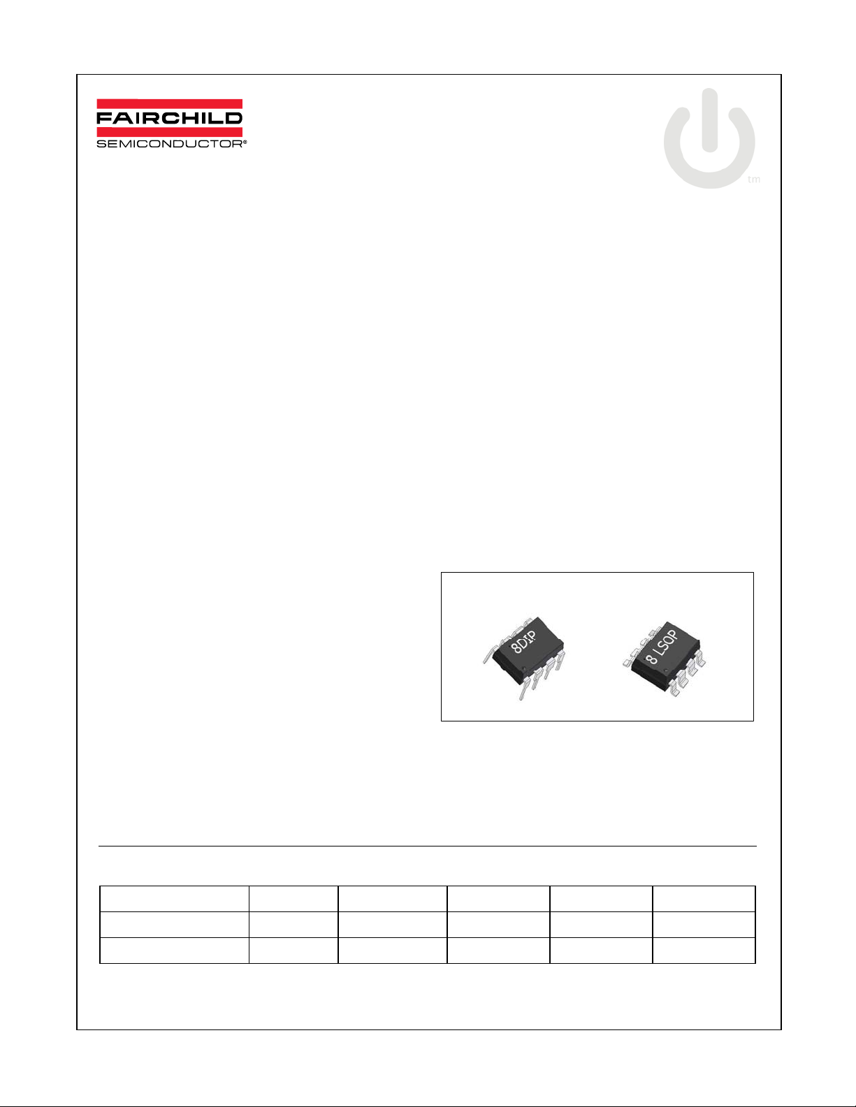
FSQ211
Green Mode Fairchild Power Switch (FPS
FSQ211 ⎯ Green Mode Fairchild Power Switch (FPS
April 2007
TM
)
Features
Internal Avalanche-Rugged SenseFET
Precision Fixed Operating Frequency (67KHz)
Burst-Mode Operation
Internal Start-up Circuit
Pulse-by-Pulse Current Limiting
Overload Protection (OLP)
Internal Thermal Shutdown Function (TSD)
Auto-Restart Mode
Under-Voltage Lockout (UVLO) with Hysteresis
Built-in Soft-Start
Secondary-Side Regulation
Applications
Charger & Adapter for Mobile Phone, PDA, & MP3
Auxiliary Power for White Goods, PC, C-TV, &
Monitor
Related Application Notes
AN-4137 Design Guidelines for Off-line Flyback
Converters using FPS™
AN-4141 Troubleshooting and Design Tips for
Fairchild Power Switch (FPS™) Flyback Applications
AN-4147 Design Guidelines for RCD Snubber of
Flyback
AN-4134Design Guidelines for Off-line Forward
Converters using FPS™
AN-4138Design Considerations for Battery Charger
Using Green Mode Fairchild Power Switch (FPS™)
Description
The FSQ211 consists of an integrated Pulse Width
Modulator (PWM) and SenseFET, specifically designed
for high-performance, off-line Switch Mode Power
Supplies (SMPS) with minimal external components.
This device is an integrated high-voltage power
switching regulator that combines a VDMOS SenseFET
with a voltage mode PWM control block. The integrated
PWM controller features include a fixed oscillator, Under
Voltage Lockout (UVLO) protection, Leading Edge
Blanking (LEB), an optimized gate turn-on/turn-off
driver, Thermal Shutdown (TSD) protection, and
temperature compensated precision-current sources for
loop compensation and fault protection circuitry.
When compared to a discrete MOSFET and controller or
RCC switching converter solution, the FSQ211 device
reduces total component count and design size and
weight, while increasing efficiency, productivity, and
system reliability. This device provides a basic platform
well suited for cost-effective flyback converters.
TM
)
Ordering Information
Part Number Package Top Mark BV
FSQ211 8DIP
FSQ211L 8LSOP
FPSTM is a trademark of Fairchild Semiconductor Corporation
© 2007 Fairchild Semiconductor Corporation www.fairchildsemi.com
FSQ211 Rev. 1.0.0
Q211
Q211L
f
DSS
650V 67KHz
650V 67KHz
R
OSC
DS(ON)
18Ω
18Ω
Page 2
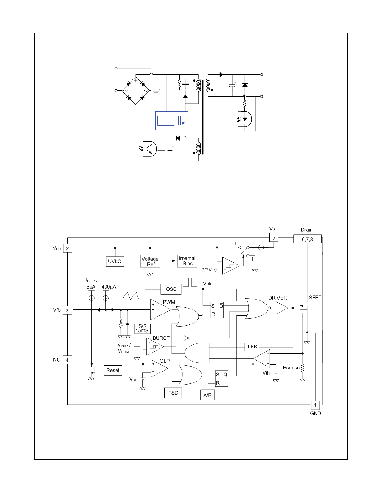
Typical Application
AC
IN
Drain
Vstr
PWM
FSQ211 ⎯ Green Mode Fairchild Power Switch (FPS
DC
OUT
Internal Block Diagram
Vfb Vcc
Figure 1. Typical Flyback Application
GND
TM
)
Figure 2. Functional Block Diagram of FSQ211
© 2007 Fairchild Semiconductor Corporation www.fairchildsemi.com
FSQ211 Rev. 1.0.0 2
Page 3
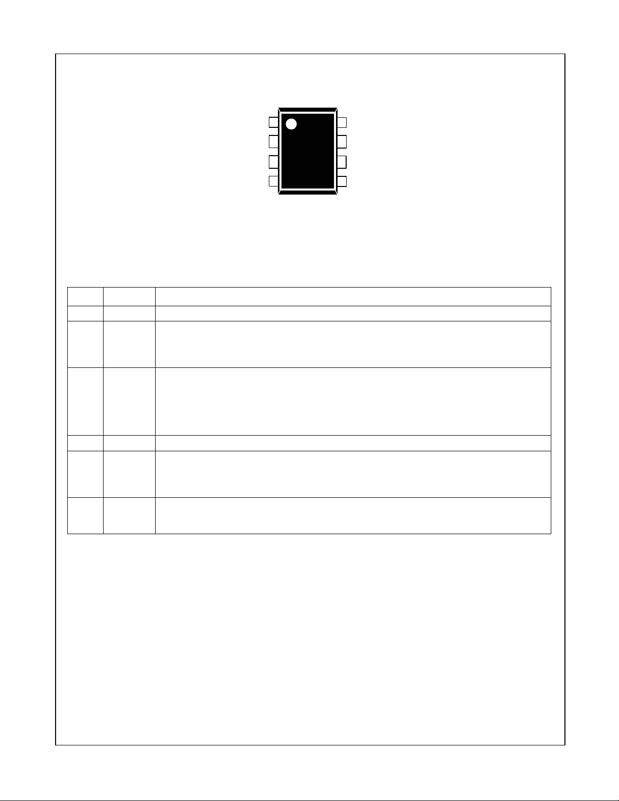
Pin Assignments
FSQ211 ⎯ Green Mode Fairchild Power Switch (FPS
1
2
Vcc
Vfb
3
45
NC
Drain
8GND
Drain
7
6
Drain
Vstr
Figure 3. Pin Configuration (Top View)
Pin Definitions
Pin Name Description
1
2
3
4
5
6,7,8 Drain
GND
V
CC
V
FB
NC
Vstr
Ground. SenseFET source terminal on primary side and internal control ground.
Positive supply voltage input. Although connected to an auxiliary transformer winding,
current is supplied from pin 5 (Vstr) via an internal switch during startup (see Block Diagram). It
is not until V
reaches the UVLO upper threshold (9V), that the internal start-up switch opens
CC
and device power is supplied via the auxiliary transformer winding.
Feedback. Inverts input to the PWM comparator with its normal input level between 0.5V and
2.5V. It has a 0.4mA current source connected internally, while a capacitor and opto-coupler
are typically connected externally. A feedback voltage of 4.5V triggers overload protection
(OLP). There is a time delay while charging external capacitor C
internal 5µA current source. This time delay prevents false triggering under transient
conditions, but allows the protection mechanism to operate under true overload conditions.
No Connection.
Start-up. This pin connects directly to the rectified AC line voltage source. At start-up, the
internal switch supplies internal bias and charges an external storage capacitor placed
between the VCC pin and ground. Once the VCC reaches 9V, the internal switch stops charging
the capacitor.
SenseFET Drain. The drain pins are designed to connect directly to the primary lead of the
transformer and are capable of switching a maximum of 650V. Minimizing the length of the
trace connecting these pins to the transformer decreases leakage inductance.
TM
)
from 3V to 4.5V using an
FB
© 2007 Fairchild Semiconductor Corporation www.fairchildsemi.com
FSQ211 Rev. 1.0.0 3
Page 4
FSQ211 ⎯ Green Mode Fairchild Power Switch (FPS
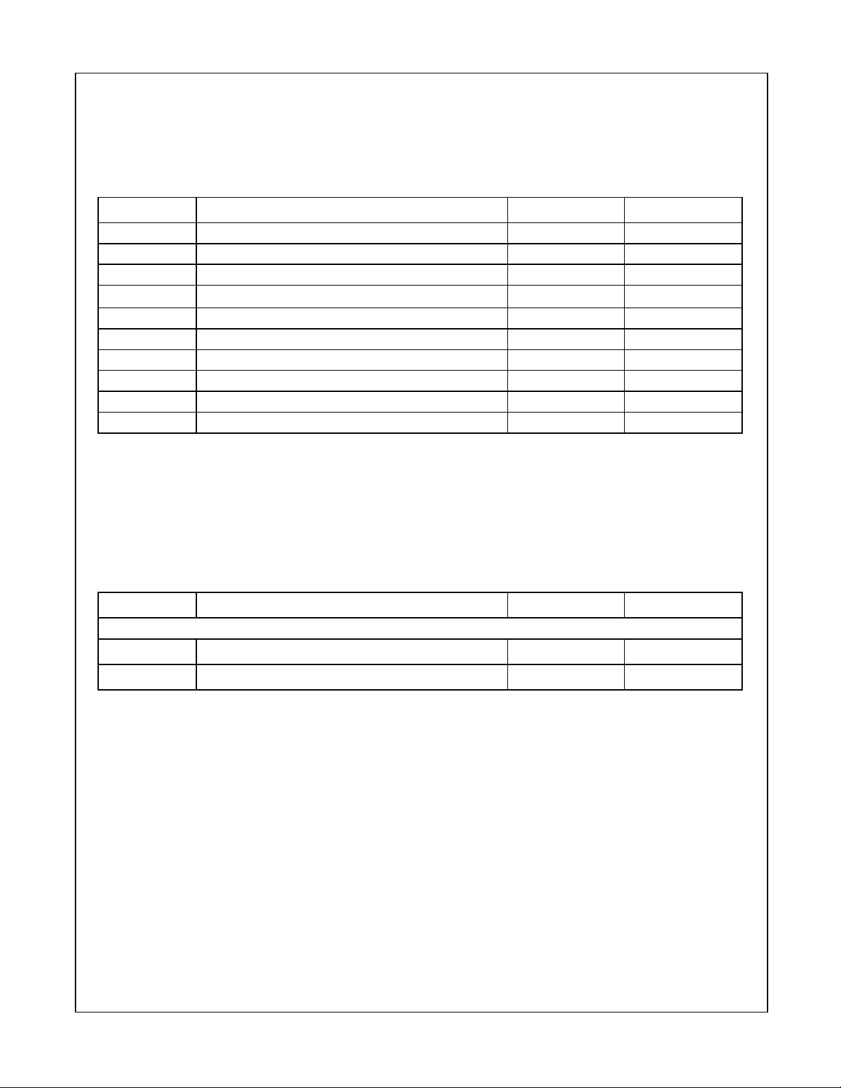
Absolute Maximum Ratings
Stresses exceeding the absolute maximum ratings may damage the device. The device may not function or be
operable above the recommended operating conditions and stressing the parts to these levels is not recommended.
In addition, extended exposure to stresses above the recommended operating conditions may affect device reliability.
The absolute maximum ratings are stress ratings only. T
Symbol Parameter Value Unit
V
Drain Pin Voltage 650 V
DRAIN
V
Vstr Pin Voltage 650 V
STR
VDG Drain-Gate Voltage 650 V
VGS Gate-Source Voltage
VCC Supply Voltage 20 V
VFB Feedback Voltage Range -0.3 to V
PD Total Power Dissipation 1.40 W
TJ Operating Junction Temperature Internally limited °C
TA Operating Ambient Temperature -25 to +85 °C
T
Storage Temperature -55 to +150 °C
STG
Notes:
1. Repetitive rating: Pulse width is limited by maximum junction temperature.
2. L = 24mH, starting T
= 25°C.
J
=25°C unless otherwise specified.
A
±20
STOP
V
V
TM
)
Thermal Impedance
TA=25°C unless otherwise specified.
Symbol Parameter Value Unit
8DIP
θJA
θJC
Notes:
3. Free standing with no heatsink; without copper clad. Measurement condition – Just before junction temperature
T
enters into OTP.
J
4. Measured on the DRAIN pin close to plastic interface.
5. All items are tested with the JEDEC standards: JESD 51-2 and 51-10 (DIP).
Junction-to-Ambient Thermal Impedance
Junction-to-Case Thermal Impedance
(3)
(4)
89 °C/W
14 °C/W
© 2007 Fairchild Semiconductor Corporation www.fairchildsemi.com
FSQ211 Rev. 1.0.0 4
Page 5
FSQ211 ⎯ Green Mode Fairchild Power Switch (FPS
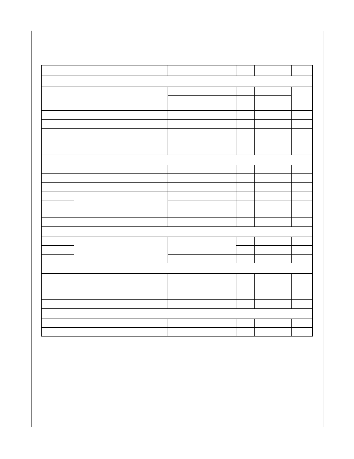
Electrical Characteristics
TA=25°C unless otherwise specified,
Symbol Parameter Conditions Min. Typ. Max. Unit
SENSEFET SECTION
VDS=650V, VGS=0V 25
I
Zero-Gate-Voltage Drain Current
DSS
R
Drain-Source On-State Resistance
DS(ON)
VDS=520V, VGS=0V,
=125°C
T
C
(6)
VGS=10V, ID=0.2A 18 25 Ω
200
gfs Forward Trans-Conductance VDS=50V, ID=0.2A 1.0 1.3 S
C
Input Capacitance 162
ISS
C
Output Capacitance 18
OSS
C
Reverse Transfer Capacitance
RSS
VGS=0V, VDS=25V,
f=1MHz
3.8
CONTROL SECTION
f
Switching Frequency 61 67 73 KHz
OSC
Δf
Switching Frequency Variation
OSC
D
Maximum Duty Cycle 60 67 74 %
MAX
V
V
START
V
STOP
UVLO Threshold Voltage
(7)
-25°C ≤ TA ≤ 85°C ±5 ±10 %
=GND 8 9 10 V
FB
VFB=GND 6 7 8 V
IFB Feedback Source Current 0V ≤ VFB ≤ 3V 0.35 0.40 0.45 mA
t
Internal Soft-Start Time 10 15 20 ms
S/S
BURST-MODE SECTION
V
0.6 0.7 0.8 V
BURH
V
BURL
V
BUR(HYS)
Burst-Mode Voltage
=25°C
T
J
0.45 0.55 0.65 V
Hysteresis 150 mV
PROTECTION SECTION
I
Peak Current Limit di/dt= 65mA/µs 0.32 0.38 0.44 A
LIM
TSD Thermal Shutdown Temperature
(8)
125 145 °C
VSD Shutdown Feedback Voltage 4.0 4.5 5.0 V
I
Shutdown Delay Current 3V ≤ VFB ≤ VSD 4 5 6 µA
DELAY
TOTAL DEVICE SECTION
IOP Operating Supply Current
(control part only)
ICH Start-Up Charging Current VCC=0V , V
VCC ≤ 16V 1.5 3.0 mA
=50V 450 550 650 µA
STR
Notes:
6. Pulse test: Pulse width ≤ 300us, duty ≤ 2%.
7. These parameters, although guaranteed, are tested in EDS (wafer test) process.
8. These parameters, although guaranteed, are not 100% tested in production.
µA
pF
TM
)
© 2007 Fairchild Semiconductor Corporation www.fairchildsemi.com
FSQ211 Rev. 1.0.0 5
Page 6
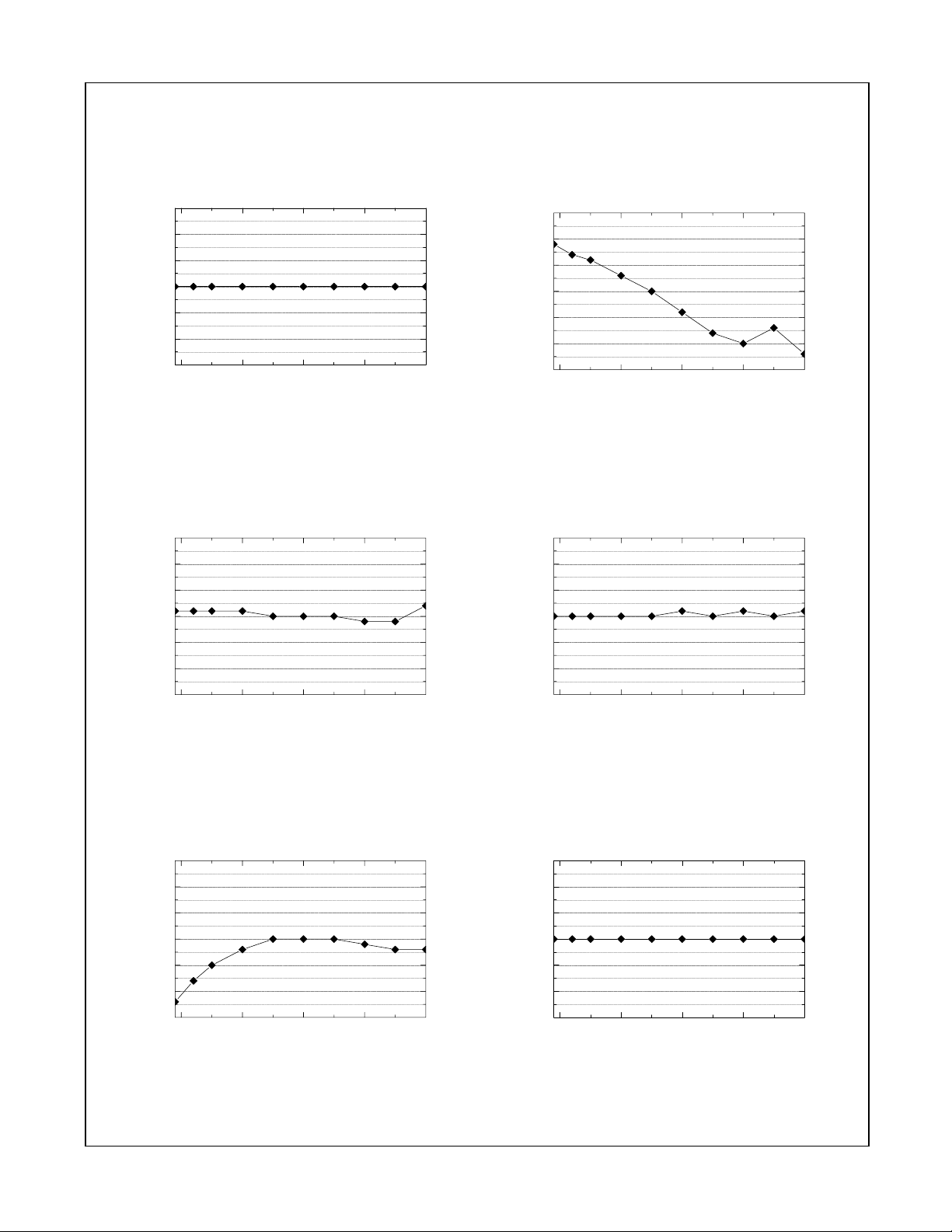
Typical Performance Characteristics
These characteristic graphs are normalized at T
= 25°C.
A
FSQ211 ⎯ Green Mode Fairchild Power Switch (FPS
1.15
1.10
1.05
1.00
REF
V
0.95
0.90
0.85
-50 0 50 100 150
Temperature [°C]
Figure 4. Reference Voltage (V
1.15
1.10
1.05
1.00
OP
I
0.95
0.90
0.85
-50 0 50 100 150
) vs. TA Figure 5. Operating Supply Current (IOP) vs. TA
REF
Temperature [°C]
1.15
1.10
1.05
1.00
STAART
V
0.95
0.90
0.85
-50 0 50 100 150
1.15
1.10
1.05
1.00
STOP
V
0.95
0.90
0.85
-50 0 50 100 150
TM
)
Temperature [°C]
Figure 6. Start Threshold Voltage (V
) vs. TA Figure 7. Stop Threshold Voltage (V
START
Temperature [°C]
STOP
) vs. TA
1.15
1.10
1.05
1.00
OSC
f
0.95
0.90
0.85
-50 0 50 100 150
Temperature [°C]
1.15
1.10
1.05
1.00
MAX
D
0.95
0.90
0.85
-50 0 50 100 150
Temperature [°C]
Figure 8. Operating Frequency (f
© 2007 Fairchild Semiconductor Corporation www.fairchildsemi.com
FSQ211 Rev. 1.0.0 6
) vs. TA Figure 9. Maximum Duty Cycle (D
OSC
) vs. TA
MAX
Page 7
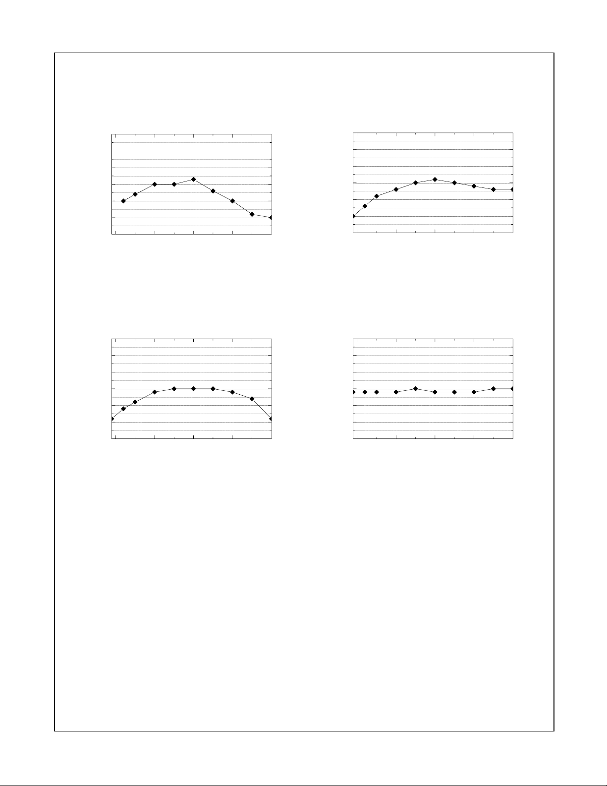
Typical Performance Characteristics (Continued)
These characteristic graphs are normalized at T
= 25°C.
A
FSQ211 ⎯ Green Mode Fairchild Power Switch (FPS
1.15
1.10
1.05
1.00
LIM
I
0.95
0.90
0.85
-50 0 50 100 150
Temperature [°C]
Figure 10. Peak Current Limit (I
1.15
1.10
1.05
1.00
FB
I
0.95
0.90
0.85
-50 0 50 100 150
Temperature [°C]
) vs. TA Figure 11. Feedback Source Current (IFB) vs. TA
LIM
1.15
1.10
1.05
1.00
DELAY
I
0.95
0.90
0.85
-50 0 50 100 150
1.15
1.10
1.05
SD
1.00
V
0.95
0.90
0.85
-50 0 50 100 150
TM
)
Temperature [°C]
Figure 12. Shutdown Delay Current (I
) vs. TA Figure 13. Shutdown Feedback Voltage (VSD) vs. TA
DELAY
Temperature [°C]
© 2007 Fairchild Semiconductor Corporation www.fairchildsemi.com
FSQ211 Rev. 1.0.0 7
Page 8
FSQ211 ⎯ Green Mode Fairchild Power Switch (FPS
Functional Description
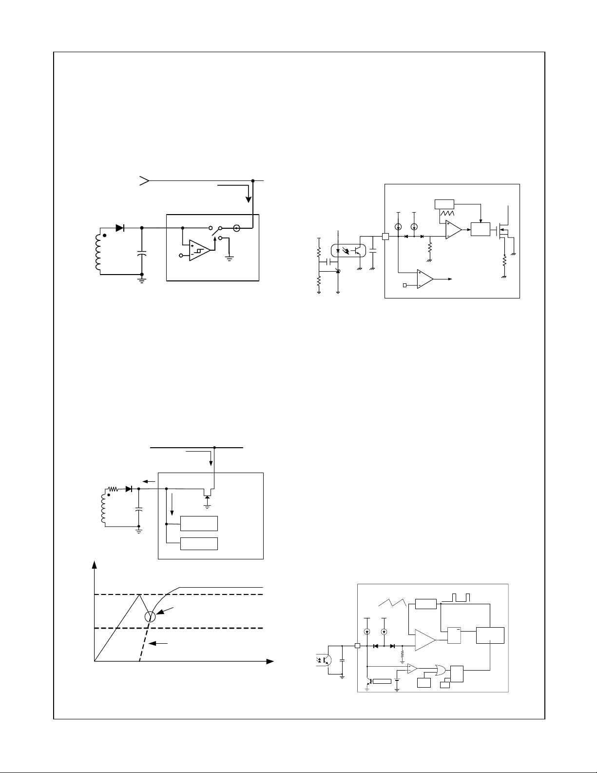
1. Start-up: At start-up, the internal high-voltage current
source supplies the internal bias and charges the
external V
case of the FSQ211, when V
starts switching and the internal high-voltage current
source stops charging the capacitor. The device is in
normal operation provided V
After start-up, the bias is supplied from the auxiliary
transformer winding.
Calculating the V
design with the FSQ211. At initial start-up, the maximum
value of start operating current I
which supplies current to UVLO and V
charging current I
– 100µA. After V
the bias winding supplies V
When the bias winding voltage is not sufficient, the V
level decreases to the UVLO stop voltage and the
internal current source is activated again to charge the
V
capacitor. To prevent this VCC fluctuation
CC
(charging/discharging), the V
chosen with a value between 10µF and 47µF.
V
CC
V
START
V
STOP
Figure 15. Charging V
capacitor, as shown in Figure 14. In the
CC
reaches 9V, the device
CC
does not drop below 7V.
CC
VIN,dc
I
STR
Vstr
V
cc
9V/7V
L
H
Figure 14. Internal Start-up Circuit
capacitor is an important step in a
CC
is about 100µA,
VCC
CC
VIN, dc
I
Vcc=ISTR-ISTART
I
Vcc=ISTR-ISTART
UVLO
STR
of the VCC capacitor is equal to I
reaches the UVLO start voltage, only
current to the device.
CC
capacitor should be
CC
I
STR
V
CC
I
START
UVLO
V
REF
VCCmust not dr op
below V
STOP
Bias winding
volt age
Capacitor Through Vstr
CC
blocks. The
REF
Vst r
J-F ET
t
STR
CC
2. Feedback Control: The FSQ211 is a voltage-mode
controlled device, as shown in Figure 16. Usually, an
opto-coupler and shunt regulator, like KA431, are used
to implement the feedback network. The feedback
voltage is compared with an internally generated
sawtooth waveform. This directly controls the duty cycle.
When the shunt regulator reference pin voltage exceeds
the internal reference voltage of 2.5V, the opto-coupler
LED current increases, the feedback voltage V
pulled down, and it reduces the duty cycle. This
happens when the input voltage increases or the output
load decreases.
VccV
5µA 0 .40mA
KA431
V
fb
4
+
C
fb
V
FB
-
V
SD
V
o
OSC
ref
Gate
driver
R
OLP
Figure 16. PWM and Feedback Circuit
3. Leading Edge Blanking (LEB): The instant the
internal SenseFET is turned on, the primary-side
capacitance and secondary-side rectifier diode reverse
recovery typically cause a high-current spike through the
SenseFET. Excessive voltage across the R
leads to incorrect pulse-by-pulse current limit protection.
To avoid this, a leading edge blanking (LEB) circuit
SENSE
disables the pulse-by-pulse current limit protection block
for a fixed time (t
) after the SenseFET turns on.
LEB
4. Protection Circuit: The FSQ211 has several
protective functions, such as overload protection (OLP),
under-voltage lockout (UVLO), and thermal shutdown
(TSD). Because these protection circuits are fully
integrated inside the IC without external components,
reliability is improved without increasing costs. Once a
fault condition occurs, switching is terminated and the
SenseFET remains off. This causes V
V
reaches the UVLO stop voltage V
CC
to fall. When
CC
(7V), the
STOP
protection is reset and the internal high-voltage current
source charges the V
V
reaches the UVLO start voltage V
CC
capacitor via the Vstr pin. When
CC
START
(9V), the
device resumes normal operation. In this manner, the
auto-restart can alternately enable and disable the
switching of the power SenseFET until the fault
condition is eliminated.
OSC
5µA 400µA
V
fb
4
C
fb
RESET
+
-
R
OLP
4.5V
TSD
SRQ
SRQ
A/R
GATE
DRIVE R
OLP, TSD
Protec tion Block
Figure 17. Protection Block
is
FB
resistor
TM
)
© 2007 Fairchild Semiconductor Corporation www.fairchildsemi.com
FSQ211 Rev. 1.0.0 8
Page 9
FSQ211 ⎯ Green Mode Fairchild Power Switch (FPS
4.1 Overload Protection (OLP): Overload is defined as
the load current exceeding a pre-set level due to an
unexpected event. In this situation, the protection circuit
should be activated to protect the SMPS. However,
even when the SMPS is operating normally, the overload protection (OLP) circuit can be activated during the
load transition. To avoid this undesired operation, the
OLP circuit is designed to be activated after a specified
time to determine whether it is a transient situation or an
overload situation. If the output consumes more than the
maximum power determined by I
(V
) decreases below its rating voltage. This reduces
O
, the output voltage
LIM
the current through the opto-coupler LED, which also
reduces the opto-coupler transistor current, thus
increasing the feedback voltage (V
). If VFB exceeds
FB
3V, the feedback input diode is blocked and the 5µA
current source (I
V
. In this condition, VFB increases until it reaches
CC
) starts to charge CFB slowly up to
DELAY
4.5V, when the switching operation is terminated, as
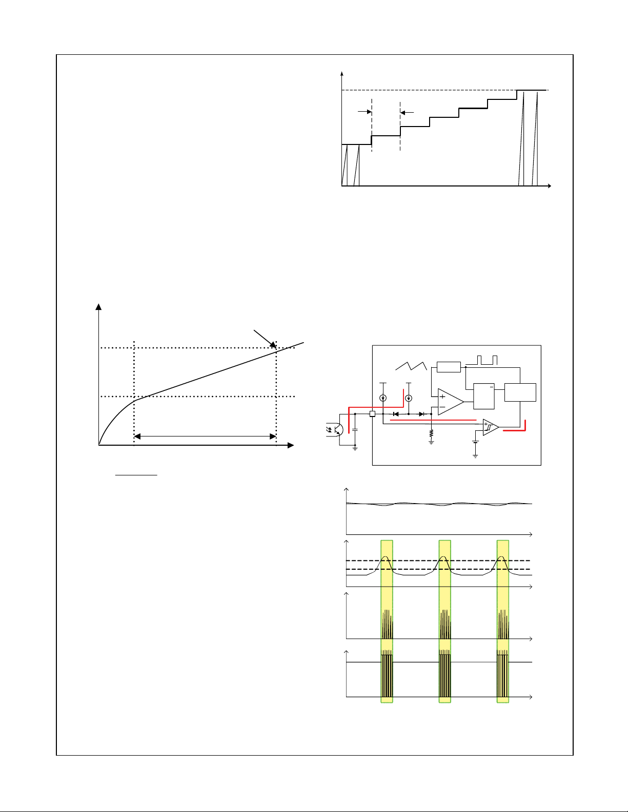
shown in Figure 18. Shutdown delay is the time required
to charge C
V
FB
from 3V to 4.5V with 5µA current source.
FB
Overload Protection
4.5V
3V
t12=CFB×(V(t2)-V(t1)) /I
t
1
tVtV
)()(
•
Ct
=m
FB
12
12
I
DELAY
DELAY
DELA Y
t
t
2
VtVVtVAI
5.4)(,3)(,5;
===
21
Figure 18. Overload Protection (OLP)
4.2 Thermal Shutdown (TSD): The SenseFET and the
control IC are integrated, making it easier for the control
IC to detect the temperature of the SenseFET. When
the temperature exceeds approximately 145°C, thermal
shutdown is activated.
5. Soft-Start: The FPS has an internal soft-start circuit
that slowly increases the feedback voltage, together with
the SenseFET current, right after it starts up. The typical
soft-start time is 15ms, as shown in Figure 19, where
progressive increment of the SenseFET current is
allowed during the start-up phase. Soft-start circuit
progressively increases current limits to establish proper
working conditions for transformers, inductors,
capacitors, and switching device. It also helps prevent
transformer saturation and reduces the stress on the
secondary diode.
Drain current
I
LIM
2.14ms
7steps
Figure 19. Internal Soft-Start
6. Burst Operation: To minimize the power dissipation
in standby mode, the FSQ211 enters burst mode
operation. As the load decreases, the feedback voltage
decreases. The device automatically enters burst mode
when the feedback voltage drops below V
BURL
(0.55V).
At this point, switching stops and the output voltages
start to drop. This causes the feedback voltage to rise.
Once is passes V
(0.70V), switching starts again.
BURH
The feedback voltage falls and the process repeats.
Burst mode operation alternately enables and disables
switching of the power MOSFET to reduce the switching
loss in the standby mode.
OSC
GATE
DR IVE R
on/off
Burs t Oper ation Bloc k
V
fb
4
5µA 4 00µA
SRQ
0.70V
/0.55V
Figure 20. Burst Operation Block
V
o
set
Vo
V
FB
0.7V
0.55V
I
ds
V
ds
t
Figure 21. Burst Operation Function
TM
)
© 2007 Fairchild Semiconductor Corporation www.fairchildsemi.com
FSQ211 Rev. 1.0.0 9
Page 10
FSQ211 ⎯ Green Mode Fairchild Power Switch (FPS
Application Tips
Methods of Reducing Audible Noise
Switching mode power converters have electronic and
magnetic components that generate audible noises
when the operating frequency is in the range of
20~20,000Hz. Even though they operate above 20kHz,
they can make noise depending on the load condition.
Designers can employ several methods to reduce noise.
Glue or Varnish
The most common method involves using glue or
varnish to tighten magnetic components. The motion of
core, bobbin and coil, and the chattering or
magnetostriction of core, can cause the transformer to
produce audible noise. The use of rigid glue and varnish
helps reduce the transformer noise, but can crack the
core. This is because sudden changes in the ambient
temperature cause the core and the glue to expand or
shrink at a different rate.
Ceramic Capacitor
Using a film capacitor instead of a ceramic capacitor as
a snubber capacitor is another noise-reduction option.
Some dielectric materials show a piezoelectric effect,
depending on the electric field intensity. Therefore, a
snubber capacitor becomes one of the most significant
sources of audible noise. It is possible to use a Zener
clamp circuit instead of an RCD snubber for higher
efficiency as well as lower audible noise.
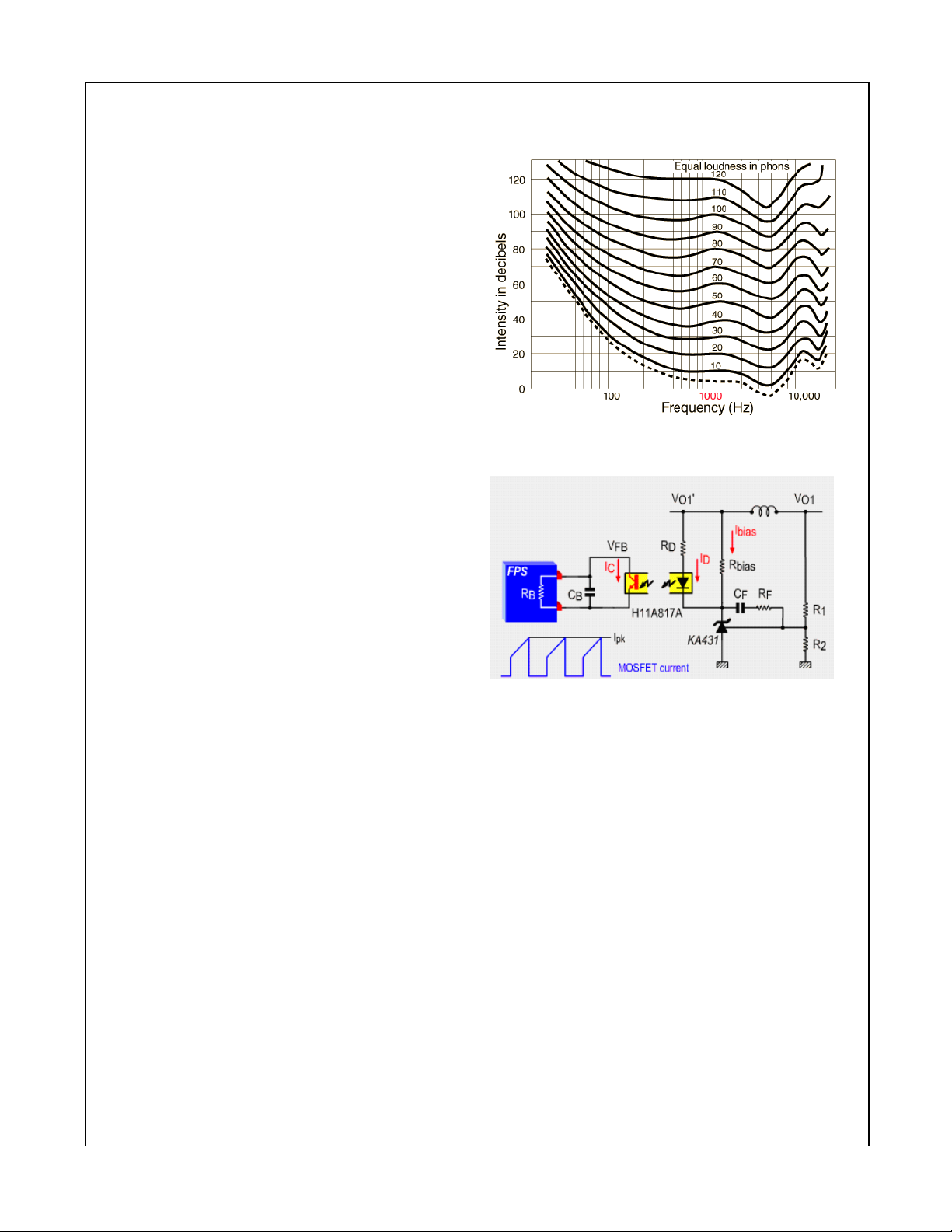
Figure 22. Equal Loudness Curves
TM
)
Adjusting Sound Frequency
Moving the fundamental frequency of noise out of
2~4kHz range is the third method. Generally, humans
are more sensitive to noise in the range of 2~4kHz.
When the fundamental frequency of noise is located in
this range, the noise is perceived as louder, although
the noise intensity level is identical (refer to Figure 22
Equal Loudness Curves).
When FPS acts in burst mode and the burst operation is
suspected to be a source of noise, this method may be
helpful. If the frequency of burst-mode operation lies in
the range of 2~4kHz, adjusting the feedback loop can
shift the burst operation frequency. To reduce the burst
operation frequency, increase a feedback gain capacitor
(C
), opto-coupler supply resistor (RD), and feedback
F
capacitor (C
(R
), as shown in Figure 23.
F
), and decrease a feedback gain resistor
B
Figure 23. Typical Feedback Network of FPS™
Other Reference Materials
AN-4134: Design Guidelines for Off-line Forward
Converters Using Fairchild Power Switch
(FPS™)
AN-4137: Design Guidelines for Off-line Flyback
Converters Using Fairchild Power Switch
(FPS™)
AN-4138: Design Considerations for Battery Charger
Using Green Mode Fairchild Power Switch
(FPS™)
AN-4140: Transformer Design Consideration for Off-line
Flyback Converters Using Fairchild Power
Switch (FPS™)
AN-4141: Troubleshooting and Design Tips for Fairchild
Power Switch (FPS™) Flyback Applications
AN-4147: Design Guidelines for RCD Snubber of
Flyback
AN-4148: Audible Noise Reduction Techniques for
FPS™ Application
© 2007 Fairchild Semiconductor Corporation www.fairchildsemi.com
FSQ211 Rev. 1.0.0 10
Page 11
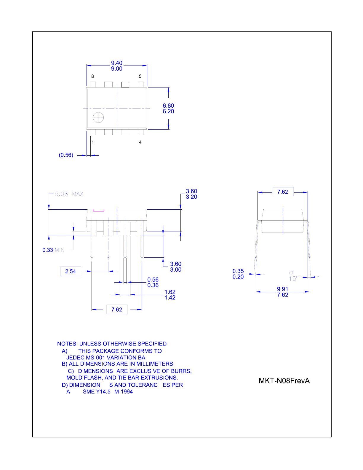
Physical Dimensions
Dimensions are in millimeters unless otherwise noted.
FSQ211 ⎯ Green Mode Fairchild Power Switch (FPS
TM
)
Figure 24. 8-Lead Dual In-line Package (DIP)
© 2007 Fairchild Semiconductor Corporation www.fairchildsemi.com
FSQ211 Rev. 1.0.0 11
Page 12
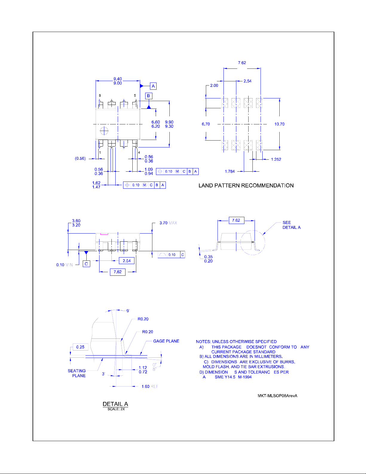
Physical Dimensions (Continued)
Dimensions are in millimeters unless otherwise noted.
FSQ211 ⎯ Green Mode Fairchild Power Switch (FPS
TM
)
Figure 25. 8-Lead LSOP
© 2007 Fairchild Semiconductor Corporation www.fairchildsemi.com
FSQ211 Rev. 1.0.0 12
Page 13
FSQ211 ⎯ Green Mode Fairchild Power Switch (FPS
TM
)
© 2007 Fairchild Semiconductor Corporation www.fairchildsemi.com
FSQ211 Rev. 1.0.0 13
 Loading...