

Page 1

FSL136MR
Green Mode Fairchild Power Switch (FPS™)
FSL136MR — Green Mode Fairchild Power Switch (FPS™)
June 2010
Features
Internal Avalanche-Rugged SenseFET (650V)
Under 50mW Standby Power Consumption at
, No-load Condition with Burst Mode
265V
AC
Precision Fixed Operating Frequency with
Frequency Modulation for Attenuating EMI
Internal Startup Circuit
Built-in Soft-Start: 15ms
Pulse-by-Pulse Current Limiting
Various Protections: Over-Voltage Protection
(OVP), Overload Protection (OLP), Output-Short
Protection (OSP), Abnormal Over-Current
Protection (AOCP), Internal Thermal Shutdown
Function with Hysteresis (TSD)
Auto-Restart Mode
Under-Voltage Lockout (UVLO)
Low Operating Current: 1.8mA
Adjustable Peak Current Limit
Applications
SMPS for VCR, STB, DVD, & DVCD Players
SMPS for Home Appliance
Adapter
Related Resources
AN-4137 — Design Guidelines for Off-line Flyback
Converters using FPS™
AN-4141 — Troubleshooting and Design Tips for
Fairchild Power Switch (FPS™) Flyback
Applications
AN-4147 — Design Guidelines for RCD Snubber of
Flyback
Description
The FSL136MR integrated Pulse Width Modulator
(PWM) and SenseFET is specifically designed for highperformance offline Switch-Mode Power Supplies
(SMPS) with minimal external components. FSL136MR
includes integrated high-voltage power switching
regulators that combine an avalanche-rugged
SenseFET with a current-mode PWM control block.
The integrated PWM controller includes: Under-Voltage
Lockout (UVLO) protection, Leading-Edge Blanking
(LEB), a frequency generator for EMI attenuation, an
optimized gate turn-on/turn-off driver, Thermal
Shutdown (TSD) protection, and temperaturecompensated precision current sources for loop
compensation and fault protection circuitry. The
FSL136MR offers good soft-start performance. When
compared to a discrete MOSFET and controller or RCC
switching converter solution, the FSL136MR reduces
total component count, design size, and weight; while
increasing efficiency, productivity, and system reliability.
This device provides a basic platform that is well suited
for the design of cost-effective flyback converters.
Maximum Output Power
230VAC ± 15%
Adapter
Notes:
1. The junction temperature can limit the maximum
2. 230V
3. Typical continuous power in a non-ventilated
(3)
19W 26W 14W 20W
output power.
or 100/115VAC with doubler.
AC
enclosed adapter measured at 50°C ambient.
(2)
85-265VAC
Open
Frame
Adapter
(1)
(3)
Open
Frame
Ordering Information
Part Number
FSL136MR -40 to +105°C FSL136MR 8-Lead, Dual Inline Package (DIP) Rail
© 2009 Fairchild Semiconductor Corporation www.fairchildsemi.com
FSL136MR • Rev. 1.0.7
Operating
Temperature Range
Top Mark Package Packing Method
Page 2
n
V
V
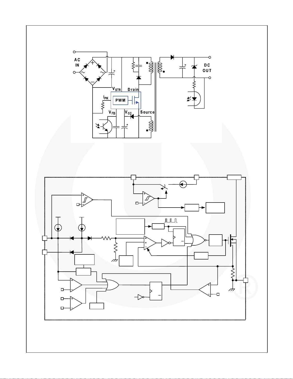
Typical Application Diagram
FSL136MR — Green Mode Fairchild Power Switch (FPS™)
Figure 1. Typical Application
Internal Block Diagram
V
BURL/VBURH
DELAY
V
CC
I
FB
On-Time
Detector
OSP
TSD
V
CC
I
3
FB
I
PK
4
V
SD
V
CC
V
OVP
2.5R
8V/12V
Frequenc y
Generator
R
Start
VCCGood
V
CC
2 6,7,8
VCCGood
STR
5
I
CH
V
REF
Int ernal
Bias
Ra ndom
OSC
SQQ
Soft
PWM
S
R
Q
Gate
Driver
LEB
AOCP
R
Q
V
AOCP
Drai
1
GND
Figure 2. Internal Block Diagram
© 2009 Fairchild Semiconductor Corporation www.fairchildsemi.com
FSL136MR • Rev. 1.0.7 2
Page 3
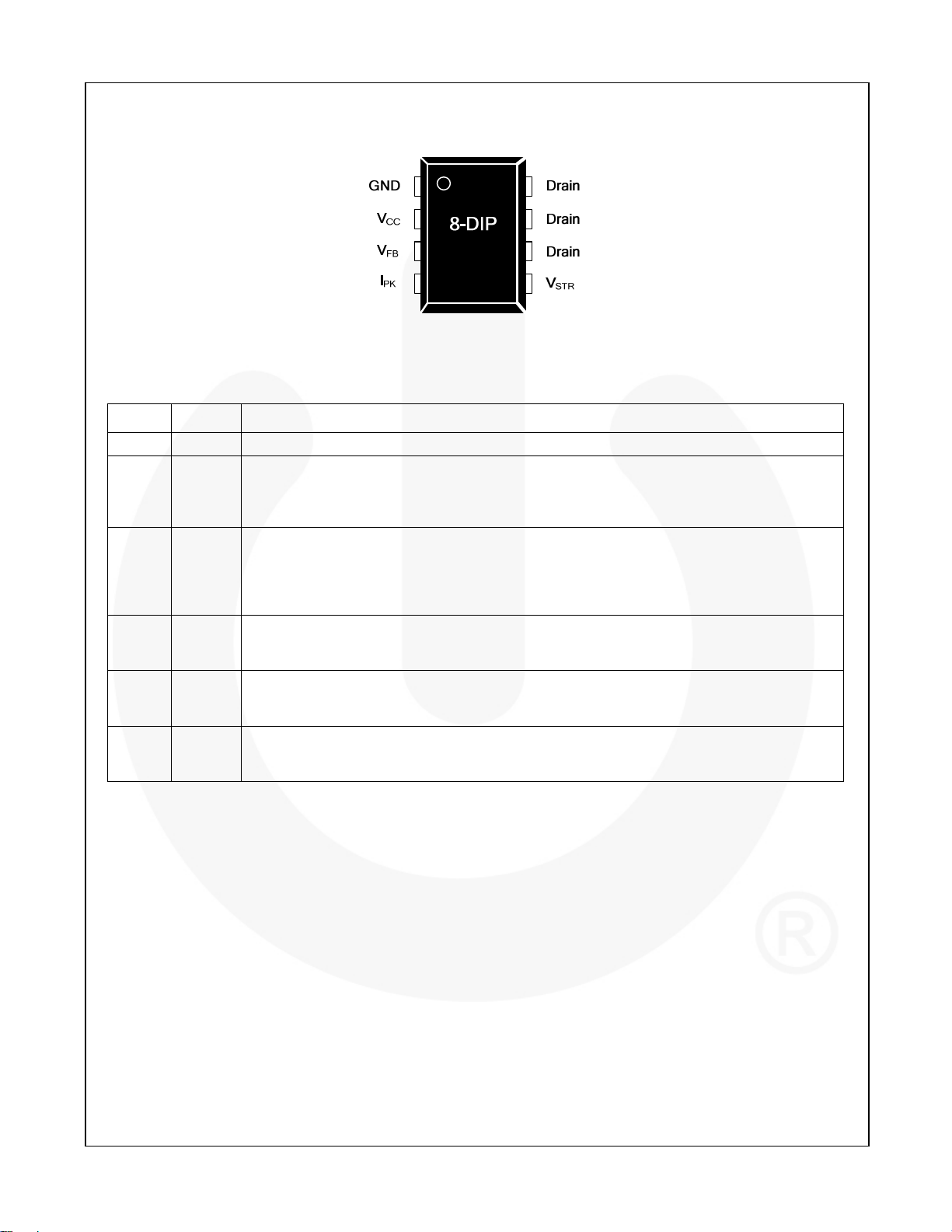
Pin Configuration
Pin Definitions
FSL136MR — Green Mode Fairchild Power Switch (FPS™)
Figure 3. Pin Configuration
Pin # Name
1 GND
2 VCC
3 VFB
4 IPK
5 V
6, 7, 8 Drain
STR
Description
Ground. SenseFET source terminal on the primary side and internal control ground.
Positive Supply Voltage Input. Although connected to an auxiliary transformer winding,
current is supplied from pin 5 (V
reaches the UVLO upper threshold (12V), the internal startup switch opens and device
V
CC
) via an internal switch during startup (see Figure 2). Once
STR
power is supplied via the auxiliary transformer winding.
Feedback Voltage. The non-inverting input to the PWM comparator, it has a 0.4mA current
source connected internally, while a capacitor and opto-coupler are typically connected
externally. There is a delay while charging external capacitor CFB from 2.4V to 6V using an
internal 5µA current source. This delay prevents false triggering under transient conditions, but
still allows the protection mechanism to operate under true overload conditions.
Peak Current Limit. Adjusts the peak current limit of the SenseFET. The feedback 0.4mA
current source is diverted to the parallel combination of an internal 6k resistor and any
external resistor to GND on this pin to determine the peak current limit.
Startup. Connected to the rectified AC line voltage source. At startup, the internal switch
supplies internal bias and charges an external storage capacitor placed between the VCC pin
and ground. Once V
reaches 12V, the internal switch is opened.
CC
Drain. Designed to connect directly to the primary lead of the transformer and capable of
switching a maximum of 650V. Minimizing the length of the trace connecting these pins to the
transformer decreases leakage inductance.
© 2009 Fairchild Semiconductor Corporation www.fairchildsemi.com
FSL136MR • Rev. 1.0.7 3
Page 4

FSL136MR — Green Mode Fairchild Power Switch (FPS™)
Absolute Maximum Ratings
Stresses exceeding the absolute maximum ratings may damage the device. The device may not function or be
operable above the recommended operating conditions and stressing the parts to these levels is not recommended.
In addition, extended exposure to stresses above the recommended operating conditions may affect device
reliability. The absolute maximum ratings are stress ratings only. T
Symbol Parameter Min. Max. Unit
V
V
STR
VDS Drain Pin Voltage -0.3 650.0 V
VCC Supply Voltage 26 V
VFB Feedback Voltage Range -0.3 12.0 V
ID Continuous Drain Current 3 A
IDM Drain Current Pulsed
EAS Single Pulsed Avalanche Energy
PD Total Power Dissipation 1.5 W
TJ Operating Junction Temperature Internally Limited °C
TA Operating Ambient Temperature -40 +105 °C
T
Storage Temperature -55 +150 °C
STG
ESD
ΘJA
ΘJC
ΘJT
Notes:
4. Repetitive rating: pulse width limited by maximum junction temperature.
5. L=51mH, starting T
6. Meets JEDEC standards JESD 22-A114 and JESD 22-C101.
7. All items are tested with the standards JESD 51-2 and JESD 51-10.
8. Θ
9. Θ
free-standing, with no heat-sink, under natural convection.
JA
junction-to-lead thermal characteristics under ΘJA test condition. TC is measured on the source #7 pin closed
JC
to plastic interface for Θ
10. Θ
junction-to-top of thermal characteristic under ΘJA test condition. Tt is measured on top of package. Thermo-
JT
couple is mounted in epoxy glue.
Pin Voltage -0.3 650.0 V
STR
(4)
12 A
(5)
230 mJ
Human Body Model, JESD22-A114
Charged Device Model, JESD22-C101
Junction-to-Ambient Thermal Resistance
Junction-to-Case Thermal Resistance
Junction-to-Top Thermal Resistance
=25°C.
J
thermo-couple mounted on soldering.
JA
(6)
5.0
(6)
1.5
(7,8)
(7,9)
19 °C/W
(7,10)
33.7 °C/W
= 25°C, unless otherwise specified.
J
KV
80 °C/W
© 2009 Fairchild Semiconductor Corporation www.fairchildsemi.com
FSL136MR • Rev. 1.0.7 4
Page 5
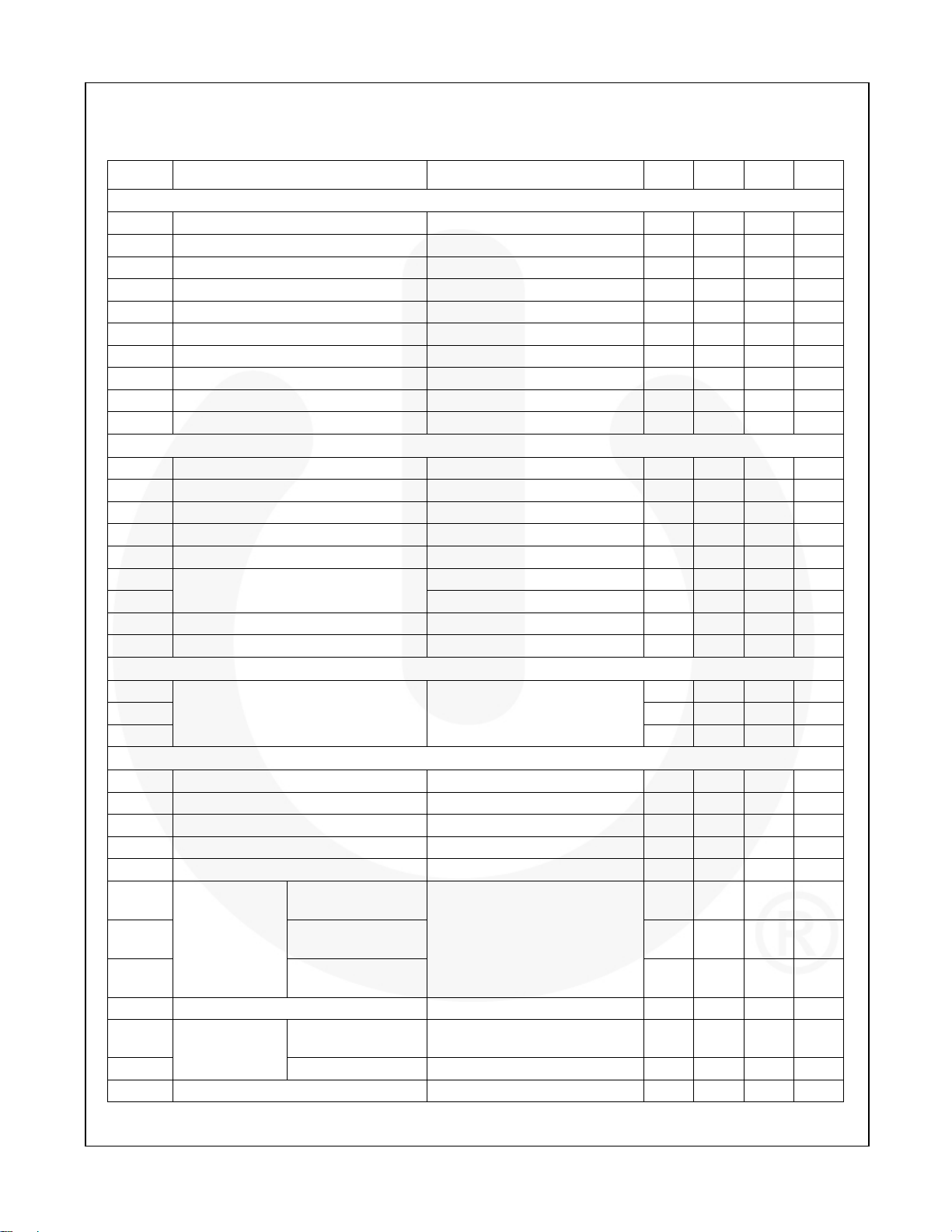
Electrical Characteristics
TA = 25°C unless otherwise specified.
Symbol Parameter Conditions Min. Typ. Max. Units
SenseFET Section
BV
Drain-Source Breakdown Voltage VCC = 0V, ID = 250µA 650 V
DSS
I
Zero Gate Voltage Drain Current VDS = 650V, VGS = 0V 250 µA
DSS
R
Drain-Source On-State Resistance VGS = 10V, VGS = 0V, TC = 25°C 3.5 4.0
DS(ON)
C
Input Capacitance VGS = 0V, VDS = 25V, f = 1MHz 290 pF
ISS
C
Output Capacitance VGS = 0V, VDS = 25V, f = 1MHz 45 pF
OSS
C
Reverse Transfer Capacitance VGS = 0V, VDS = 25V, f = 1MHz 5.5 pF
RSS
t
Turn-On Delay VDD = 350V, ID = 3.5A 12 ns
d(ON)
tr Rise Time VDD = 350V, ID = 3.5A 22 ns
t
Turn-Off Delay VDD = 350V, ID = 3.5A 20 ns
d(OFF)
tf Fall Time VDD = 350V, ID = 3.5A 19 ns
Control Section
f
Switching Frequency VDS = 650V, VGS = 0V 61 67 73 KHz
OSC
f
Switching Frequency Variation VGS = 10V, VGS = 0V, TC = 125°C ±5 ±10 %
OSC
fFM Frequency Modulation ±3 KHz
D
Maximum Duty Cycle VFB = 4V 71 77 83 %
MAX
D
Minimum Duty Cycle VFB = 0V 0 0 0 %
MIN
V
START
V
UVLO Threshold Voltage
After Turn-On 7 8 9 V
STOP
IFB Feedback Source Current VFB = 0V 320 400 480 µA
t
Internal Soft-Start Time VFB = 4V 10 15 20 ms
S/S
Burst Mode Section
V
BURH
V
0.25 0.35 0.45 V
Burst Mode Voltage T
BURL
V
150 mV
BUR(HYS)
Protection Section
I
Peak Current Limit TJ = 25°C, di/dt = 300mA/µs 1.89 2.15 2.41 A
LIM
t
Current Limit Delay Time
CLD
(11)
200 ns
VSD Shutdown Feedback Voltage VCC = 15V 5.5 6.0 6.5 V
I
Shutdown Delay Current VFB = 5V 3.5 5.0 6.5 µA
DELAY
V
Over-Voltage Protection Threshold VFB = 2V 22.5 24.0 25.5 V
OVP
11 12 13 V
0.4 0.5 0.6 V
= 25°C
J
FSL136MR — Green Mode Fairchild Power Switch (FPS™)
t
OSP
V
t
OSP_FB
V
TSD
HYS
t
© 2009 Fairchild Semiconductor Corporation www.fairchildsemi.com
FSL136MR • Rev. 1.0.7 5
Output-Short
OSP
Protection
(11)
AOCP Voltage
AOCP
Thermal
Shutdown
Hysteresis 60 °C
TSD
Leading-Edge Blanking Time
LEB
(11)
Threshold Time
T
= 25°C
J
Threshold Feedback
Voltage
Feedback Blanking
OSP Triggered When t
V
FB>VOSP
t
OSP_FB
and Lasts Longer than
Time
(11)
T
Shutdown
Temperature
(11)
300 ns
= 25°C 0.85 1.00 1.15 V
J
125 137 150 °C
ON<tOSP
1.00 1.35 µs
,
1.44 1.60 V
2.0 2.5 µs
Continued on the following page…
Page 6

Electrical Characteristics (Continued)
TA = 25°C unless otherwise specified.
Symbol Parameter Conditions Min. Typ. Max. Units
Total Device Section
I
I
Operating Supply Current
OP1
(While Switching)
Operating Supply Current
OP2
(Control Part Only)
ICH Startup Charging Current VCC = 0V 0.90 1.10 1.30 mA
V
Minimum V
STR
Supply Voltage VCC = VFB = 0V, V
STR
Note:
11. Though guaranteed by design, it is not 100% tested in production.
(11)
VCC = 14V, VFB > V
VCC = 14V, VFB < V
2.5 3.5 mA
BURH
1.8 2.5 mA
BURL
Increase 35 V
STR
FSL136MR — Green Mode Fairchild Power Switch (FPS™)
© 2009 Fairchild Semiconductor Corporation www.fairchildsemi.com
FSL136MR • Rev. 1.0.7 6
Page 7
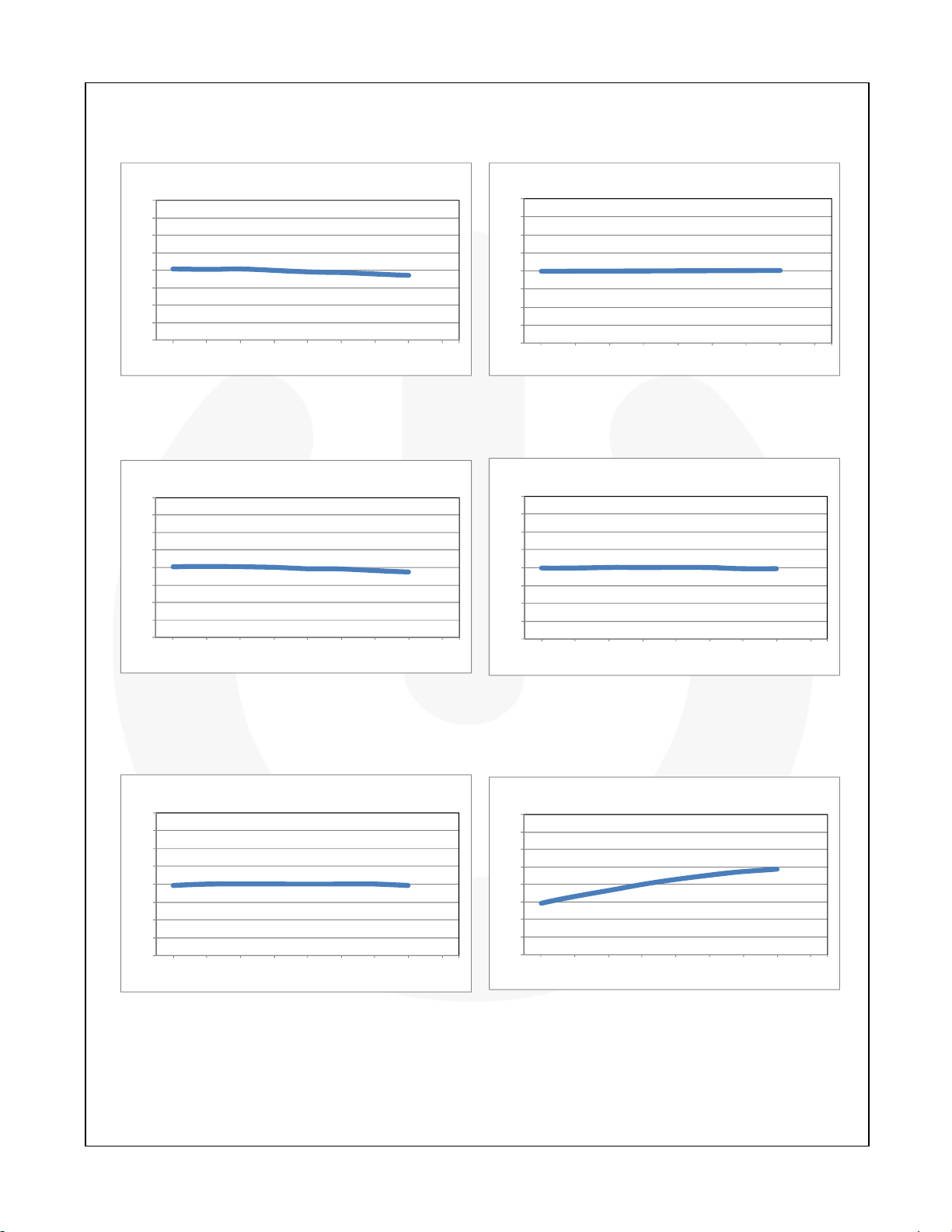
Typical Performance Characteristics
These characteristic graphs are normalized at TA=25.
FSL136MR — Green Mode Fairchild Power Switch (FPS™)
OperatingFrequency(f
1.4
1.3
1.2
1.1
1
0.9
0.8
0.7
0.6
‐40Ԩ ‐25Ԩ 0 Ԩ 25Ԩ 50Ԩ 75Ԩ 100Ԩ 120Ԩ 140Ԩ
OSC
)
1.4
1.3
1.2
1.1
1
0.9
0.8
0.7
0.6
‐40Ԩ ‐25Ԩ 0Ԩ 25Ԩ 50Ԩ 75Ԩ 100Ԩ 120Ԩ 140Ԩ
MaximumDutyCycle(D
MAX
)
Figure 4. Operating Frequency vs. Temperature Figure 5. Maximum Duty Cycle vs. Temperature
OperatingSupplyCurrent(I
1.4
1.3
1.2
1.1
1.0
0.9
0.8
0.7
0.6
‐40 ‐25 0 255075100120140
op2
)
StartThresholdVoltage(V
1.4
1.3
1.2
1.1
1.0
0.9
0.8
0.7
0.6
‐40 ‐25 0 25 50 75 100 120 140
START
)
Figure 6. Operating Supply Current vs. Temperature Figure 7. Start Threshold Voltage vs. Temperature
StopThresholdVoltage(V
1.4
1.3
1.2
1.1
1.0
0.9
0.8
0.7
0.6
‐40 ‐25 0 25 50 75 100 120 140
STOP
)
1.4
1.3
1.2
1.1
1
0.9
0.8
0.7
0.6
‐40
FeedbackSourceCurrent(IFB)
Ԩ
‐25Ԩ0Ԩ25Ԩ50Ԩ75Ԩ100Ԩ120Ԩ140
Ԩ
Figure 8. Stop Threshold Voltage vs. Temperature Figure 9. Feedback Source Current vs. Temperature
© 2009 Fairchild Semiconductor Corporation www.fairchildsemi.com
FSL136MR • Rev. 1.0.7 7
Page 8
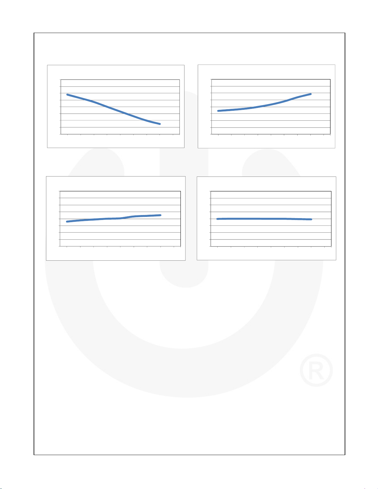
Typical Performance Characteristics (Continued)
These characteristic graphs are normalized at TA=25.
FSL136MR — Green Mode Fairchild Power Switch (FPS™)
StartupChargingCurrent(ICH)
1.4
1.3
1.2
1.1
1
0.9
0.8
0.7
0.6
‐40Ԩ ‐25Ԩ 0Ԩ 25Ԩ 50Ԩ 75Ԩ 100Ԩ 120Ԩ 14 0 Ԩ
PeakCurrentLimit(I
1.4
1.3
1.2
1.1
1
0.9
0.8
0.7
0.6
‐40Ԩ ‐25Ԩ 0Ԩ 25Ԩ 50Ԩ 75Ԩ 100Ԩ 120Ԩ 140Ԩ
LIM
)
Figure 10. Startup Charging Current vs. Temperature Figure 11. Peak Current Limit vs. Temperature
BurstOperatingSupplyCurrent(I
1.4
1.3
1.2
1.1
1.0
0.9
0.8
0.7
0.6
‐40 ‐25 0 255075100120140
Figure 12. Burst Operating Supply Current
vs. Temperature
op1
)
1.4
1.3
1.2
1.1
1
0.9
0.8
0.7
0.6
‐40Ԩ ‐25Ԩ 0 Ԩ 25Ԩ 50Ԩ 75Ԩ 100Ԩ 120Ԩ 140Ԩ
Over‐VoltageProtection(V
OVP
)
Figure 13. Over-Voltage Protection
vs. Temperature
© 2009 Fairchild Semiconductor Corporation www.fairchildsemi.com
FSL136MR • Rev. 1.0.7 8
Page 9
Functional Description
FSL136MR — Green Mode Fairchild Power Switch (FPS™)
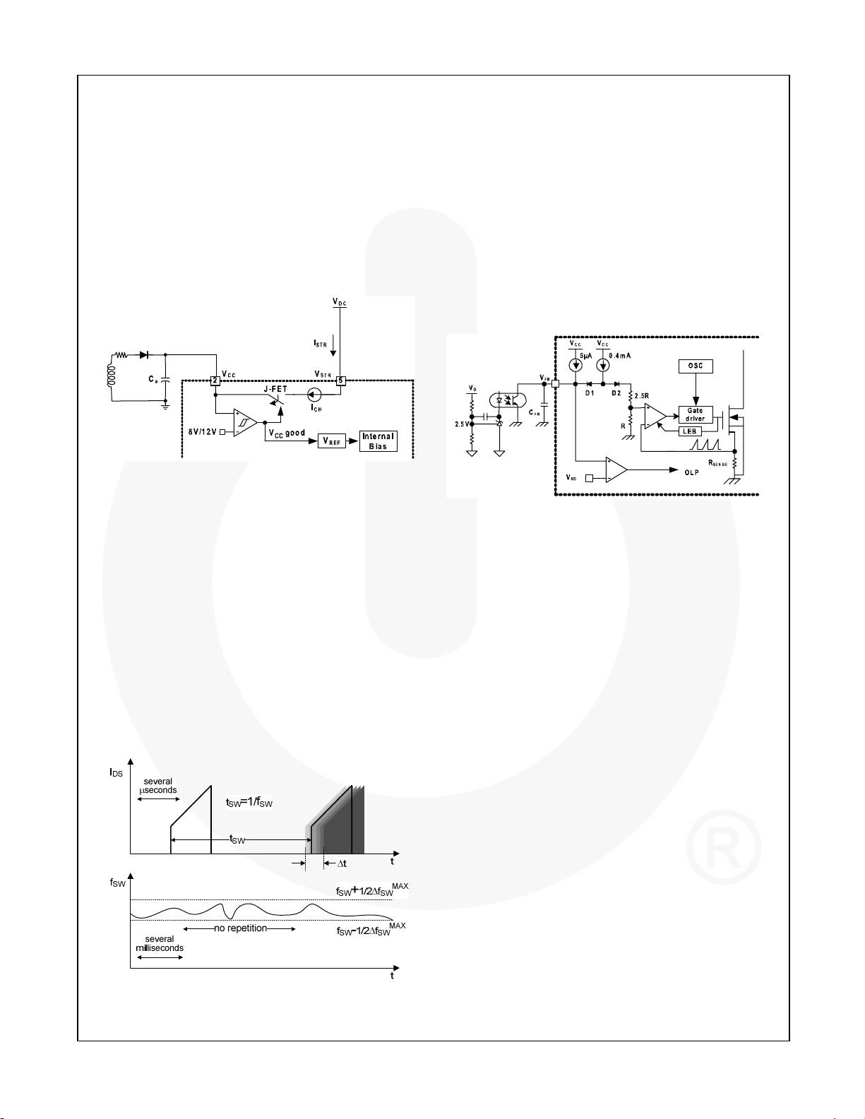
Startup
At startup, an internal high-voltage current source
supplies the internal bias and charges the external
capacitor (C
in Figure 14. When V
) connected with the VCC pin, as illustrated
A
reaches the start voltage of
CC
12V, the FPS™ begins switching and the internal highvoltage current source is disabled. The FPS continues
normal switching operation and the power is provided
from the auxiliary transformer winding unless V
goes
CC
below the stop voltage of 8V.
Figure 14. Startup Circuit
Oscillator Block
The oscillator frequency is set internally and the FPS
has a random frequency fluctuation function.
Fluctuation of the switching frequency of a switched
power supply can reduce EMI by spreading the energy
over a wider frequency range than the bandwidth
measured by the EMI test equipment. The amount of
EMI reduction is directly related to the range of the
frequency variation. The range of frequency variation is
fixed internally; however, its selection is randomly
chosen by the combination of external feedback voltage
and internal free-running oscillator. This randomly
chosen switching frequency effectively spreads the EMI
noise nearby switching frequency and allows the use of
a cost-effective inductor instead of an AC input line filter
to satisfy the world-wide EMI requirements.
Figure 15. Frequency Fluctuation Waveform
Feedback Control
FSL136MR employs current-mode control, as shown in
Figure 16. An opto-coupler (such as the FOD817A) and
shunt regulator (such as the KA431) are typically used
to implement the feedback network. Comparing the
feedback voltage with the voltage across the R
SENSE
resistor makes it possible to control the switching duty
cycle. When the shunt regulator reference pin voltage
exceeds the internal reference voltage of 2.5V, the
opto-coupler LED current increases, the feedback
voltage V
is pulled down, and the duty cycle is
FB
reduced. This typically occurs when the input voltage is
increased or the output load is decreased.
Figure 16. Pulse-Width-Modulation Circuit
Leading-Edge Blanking (LEB)
At the instant the internal SenseFET is turned on, the
primary-side capacitance and secondary-side rectifier
diode reverse recovery typically cause a high-current
spike through the SenseFET. Excessive voltage across
the R
operation in the current-mode PWM control. To counter
this effect, the FPS employs a leading-edge blanking
(LEB) circuit (see the Figure 16). This circuit inhibits the
PWM comparator for a short time (t
SenseFET is turned on.
Protection Circuits
The FPS has several protective functions, such as
overload protection (OLP), over-voltage protection
(OVP), output-short protection (OSP), under-voltage
lockout (UVLO), abnormal over-current protection
(AOCP), and thermal shutdown (TSD). Because these
various protection circuits are fully integrated in the IC
without external components, the reliability is improved
without increasing cost. Once a fault condition occurs,
switching is terminated and the SenseFET remains off.
This causes V
stop voltage, V
internal high-voltage current source charges the V
capacitor via the V
start voltage, V
operation. In this manner, the auto-restart can
alternately enable and disable the switching of the
power SenseFET until the fault condition is eliminated.
resistor leads to incorrect feedback
SENSE
) after the
LEB
to fall. When VCC reaches the UVLO
CC
(8V), the protection is reset and the
STOP
pin. When VCC reaches the UVLO
STR
(12V), the FPS resumes normal
START
CC
© 2009 Fairchild Semiconductor Corporation www.fairchildsemi.com
FSL136MR • Rev. 1.0.7 9
Page 10
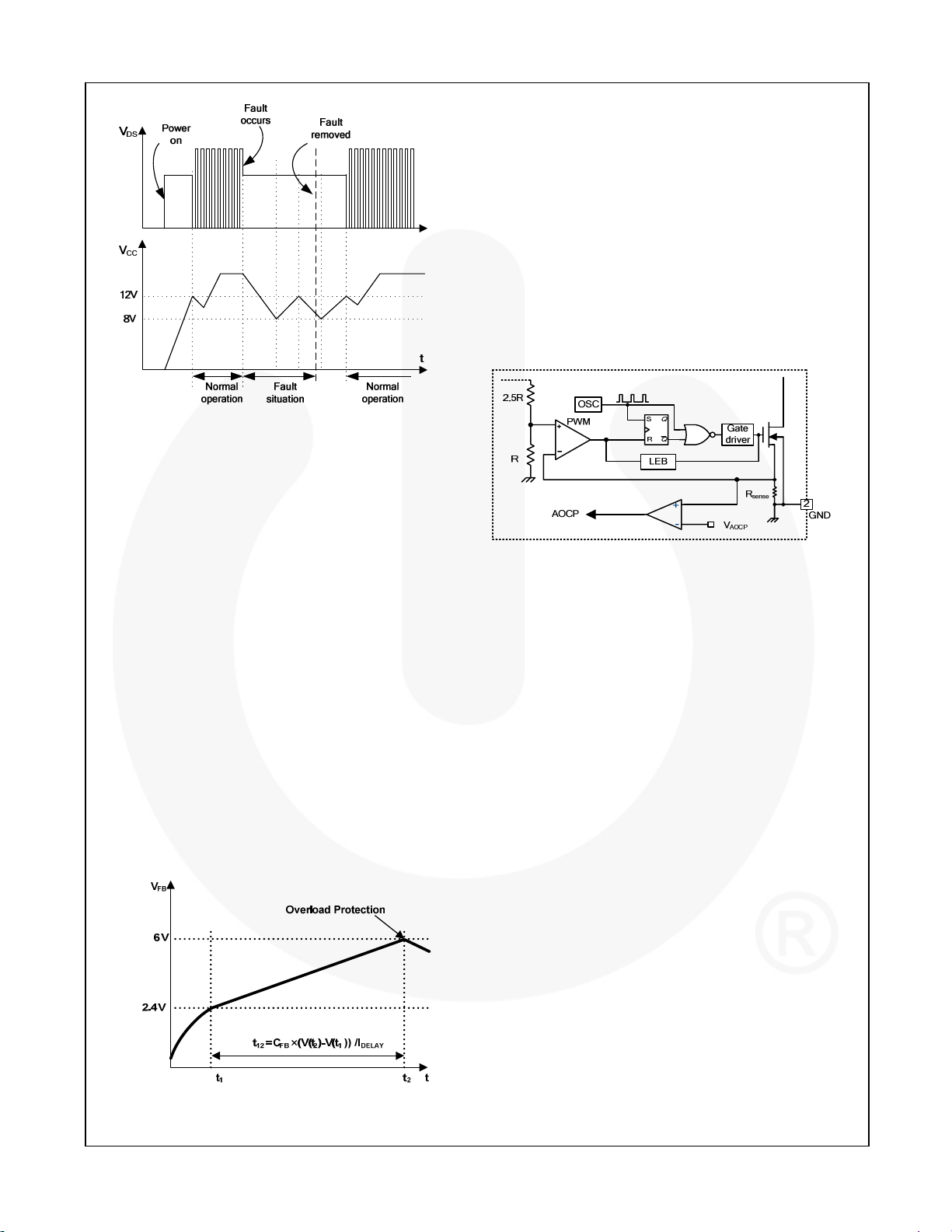
Figure 17. Auto-Restart Protection Waveforms
Overload Protection (OLP)
Overload is defined as the load current exceeding a
pre-set level due to an unexpected event. In this
situation, the protection circuit should be activated to
protect the SMPS. However, even when the SMPS is
operating normally, the overload protection (OLP) circuit
can be activated during the load transition or startup. To
avoid this undesired operation, the OLP circuit is
designed to be activated after a specified time to
determine whether it is a transient situation or a true
overload situation.
In conjunction with the I
current limit pin (if used), the
PK
current-mode feedback path limits the current in the
SenseFET when the maximum PWM duty cycle is
attained. If the output consumes more than this
maximum power, the output voltage (V
) decreases
O
below its rating voltage. This reduces the current
through the opto-coupler LED, which also reduces the
opto-coupler transistor current, thus increasing the
feedback voltage (V
). If VFB exceeds 2.4V, the
FB
feedback input diode is blocked and the 5µA current
source (I
condition, V
) slowly starts to charge CFB. In this
DELAY
increases until it reaches 6V, when the
FB
switching operation is terminated, as shown in Figure
18. The shutdown delay is the time required to charge
C
from 2.4V to 6V with 5µA current source.
FB
Abnormal Over-Current Protection (AOCP)
When the secondary rectifier diodes or the transformer
pin are shorted, a steep current with extremely high
di/dt can flow through the SenseFET during the LEB
time. Even though the FPS has OLP (Overload
Protection), it is not enough to protect the FPS in that
abnormal case, since severe current stress is imposed
on the SenseFET until OLP triggers. The FPS includes
the internal AOCP (Abnormal Over-Current Protection)
circuit shown in Figure 19. When the gate turn-on signal
is applied to the power SenseFET, the AOCP block is
enabled and monitors the current through the sensing
resistor. The voltage across the resistor is compared
with a preset AOCP level. If the sensing resistor voltage
is greater than the AOCP level, the set signal is applied
to the latch, resulting in the shutdown of the SMPS.
Figure 19. Abnormal Over-Current Protection
Thermal Shutdown (TSD)
The SenseFET and the control IC are integrated,
making it easier to detect the temperature of the
SenseFET. When the temperature exceeds
approximately 137°C, thermal shutdown is activated.
Over-Voltage Protection (OVP)
In the event of a malfunction in the secondary-side
feedback circuit or an open feedback loop caused by a
soldering defect, the current through the opto-coupler
transistor becomes almost zero. Then, V
climbs up in
FB
a similar manner to the overload situation, forcing the
preset maximum current to be supplied to the SMPS
until the overload protection is activated. Because
excess energy is provided to the output, the output
voltage may exceed the rated voltage before the
overload protection is activated, resulting in the
breakdown of the devices in the secondary side. To
prevent this situation, an over-voltage protection (OVP)
circuit is employed. In general, V
output voltage and the FPS uses V
monitoring the output voltage. If V
is proportional to the
CC
instead of directly
CC
exceeds 24V, OVP
CC
circuit is activated, resulting in termination of the
switching operation. To avoid undesired activation of
OVP during normal operation, V
should be designed
CC
to be below 24V.
FSL136MR — Green Mode Fairchild Power Switch (FPS™)
Output-Short Protection (OSP)
If the output is shorted, the steep current with extremely
high di/dt can flow through the SenseFET during the
LEB time. Such a steep current brings high-voltage
Figure 18. Overload Protection (OLP)
© 2009 Fairchild Semiconductor Corporation www.fairchildsemi.com
FSL136MR • Rev. 1.0.7 10
stress on the drain of SenseFET when turned off. To
protect the device from such an abnormal condition,
OSP detects V
V
is higher than 1.6V and the SenseFET turn-on time
FB
and SenseFET turn-on time. When the
FB
Page 11
A
=
is lower than 1.0µs, the FPS recognizes this condition
as an abnormal error and shuts down PWM switching
until V
reaches V
CC
again. An abnormal condition
START
output is shown in Figure 20.
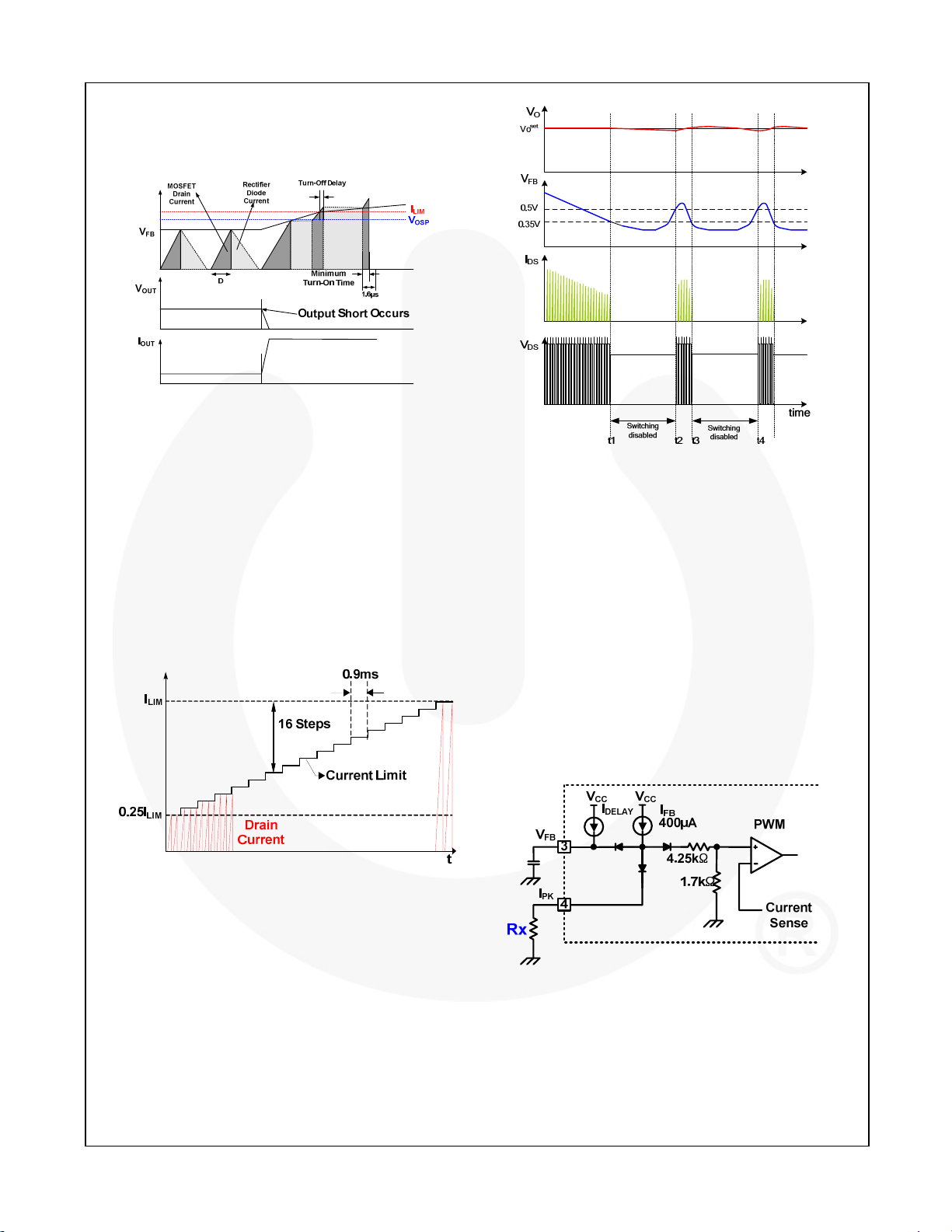
Figure 20. Output Short Waveforms (OSP)
FSL136MR — Green Mode Fairchild Power Switch (FPS™)
Soft-Start
The FPS has an internal soft-start circuit that slowly
increases the feedback voltage, together with the
SenseFET current, after it starts. The typical soft-start
time is 15ms, as shown in Figure 21, where progressive
increments of the SenseFET current are allowed during
the startup phase. The pulse width to the power
switching device is progressively increased to establish
the correct working conditions for transformers,
inductors, and capacitors. The voltage on the output
capacitors is progressively increased with the intention
of smoothly establishing the required output voltage.
Soft-start helps prevent transformer saturation and
reduce the stress on the secondary diode.
Figure 21. Internal Soft-Start
Figure 22. Burst-Mode Operation
Adjusting Peak Current Limit
As shown in Figure 23, a combined 6k internal
resistance is connected to the non-inverting lead on the
PWM comparator. An external resistance of Rx on the
current limit pin forms a parallel resistance with the 6k
when the internal diodes are biased by the main current
source of 400µA. For example, FSL136MR has a typical
SenseFET peak current limit (I
adjusted to 1.5A by inserting Rx between the I
the ground. The value of the Rx can be estimated by
the following equations:
XkΩ:6kΩ1.5A:2.15
=
6kΩ||RxX
where X is the resistance of the parallel network.
) of 2.15A. I
LIM
can be
LIM
pin and
PK
(1)
(2)
Burst Operation
To minimize power dissipation in standby mode, the
FPS enters burst mode. As the load decreases, the
feedback voltage decreases. As shown in Figure 22,
the device automatically enters burst mode when the
feedback voltage drops below V
continues until the feedback voltage drops below V
. Switching
BURH
BURL
.
Figure 23. Peak Current Limit Adjustment
At this point, switching stops and the output voltages
drop at a rate dependent on standby current load. This
causes the feedback voltage to rise. Once it passes
V
, switching resumes. The feedback voltage then
BURH
falls and the process repeats. Burst mode alternately
enables and disables switching of the SenseFET and
reduces switching loss in standby mode.
© 2009 Fairchild Semiconductor Corporation www.fairchildsemi.com
FSL136MR • Rev. 1.0.7 11
Page 12
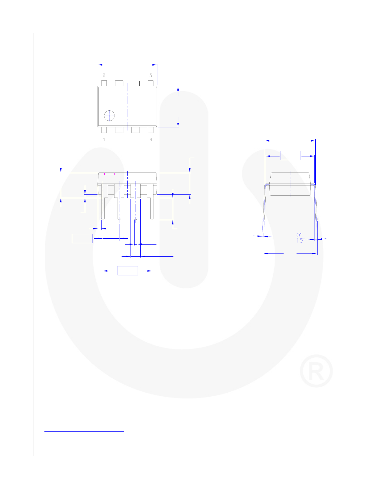
Physical Dimensions
FSL136MR — Green Mode Fairchild Power Switch (FPS™)
9.83
9.00
6.67
6.096
8.255
7.61
5.08 MAX
0.33 MIN
(0.56)
2.54
7.62
0.56
0.355
3.60
3.00
1.65
1.27
3.683
3.20
0.356
0.20
7.62
9.957
7.87
NOTES: UNLESS OTHERWISE SPECIFIED
A) THIS PACKAGE CONFORMS TO
JEDEC MS-001 VARIATION BA
B) ALL DIMENSIONS ARE IN MILLIMETERS.
C) DIMENSIONS ARE EXCLUSIVE OF BURRS,
MOLD FLASH, AND TIE BAR EXTRUSIONS.
D) DIMENSIONS AND TOLERANC
ES PER
ASME Y14.5M-1994
E) DRAWING FILENAME AND REVSION: MKT-N08FREV2.
Figure 24. 8-Lead, Dual Inline Package (DIP)
Package drawings are provided as a service to customers considering Fairchild components. Drawings may change in any manner
without notice. Please note the revision and/or date on the drawing and contact a Fairchild Semiconductor representative to verify
or obtain the most rece nt re vision. Package specifications do not expand the terms of Fairchild’s worldwide terms and conditions, specifically
the warranty therein, which covers Fairchild products.
Always visit Fairchild Semiconductor’s online packaging area for the most recent package drawings:
http://www.fairchildsemi.com/packaging/
.
© 2009 Fairchild Semiconductor Corporation www.fairchildsemi.com
FSL136MR • Rev. 1.0.7 12
Page 13
FSL136MR — Green Mode Fairchild Power Switch (FPS™)
© 2009 Fairchild Semiconductor Corporation www.fairchildsemi.com
FSL136MR • Rev. 1.0.7 13
 Loading...