

Page 1
Power Switch for
Half-Bridge Resonant
Converters
DATA SHEET
www.onsemi.com
FSFR-XS Series
Description
The FSFR−XS series includes highly integrated power switches
designed for high−efficiency half−bridge resonant converters.
Offering everything necessary to build a reliable and robust resonant
converter, the FSFR−XS series simplifies designs while improving
productivity and performance. The FSFR−XS series combines power
MOSFETs with fast−recovery type body diodes, a high−side
gate−drive circuit, an accurate current controlled oscillator, frequency
limit circuit, soft−start, and built−in protection functions. The
high−side gate−drive circuit has common−mode noise cancellation
capability, which guarantees stable operation with excellent noise
immunity. The fast−recovery body diode of the MOSFETs improves
reliability against abnormal operation conditions, while minimizing
the effect of reverse recovery. Using the zero−voltage−switching
(ZVS) technique dramatically reduces the switching losses and
significantly improves efficiency. The ZVS also reduces the switching
noise noticeably, which allows a small−sized Electromagnetic
Interference (EMI) filter.
The FSFR−XS series can be applied to resonant converter
topologies such as series resonant, parallel resonant, and LLC resonant
converters.
Features
• Variable Frequency Control with 50% Duty Cycle for Half−Bridge
Resonant Converter Topology
• High Efficiency through Zero Voltage Switching (ZVS)
• Internal UniFETt with Fast−Recovery Body Diode
• Fixed Dead Time (350 ns) Optimized for MOSFETs
• Up to 300 kHz Operating Frequency
• Auto−Restart Operation for All Protections with External LV
• Protection Functions: Over−Voltage Protection (OVP), Over−Current
Protection (OCP), Abnormal Over−Current Protection (AOCP),
Internal Thermal Shutdown (TSD)
CC
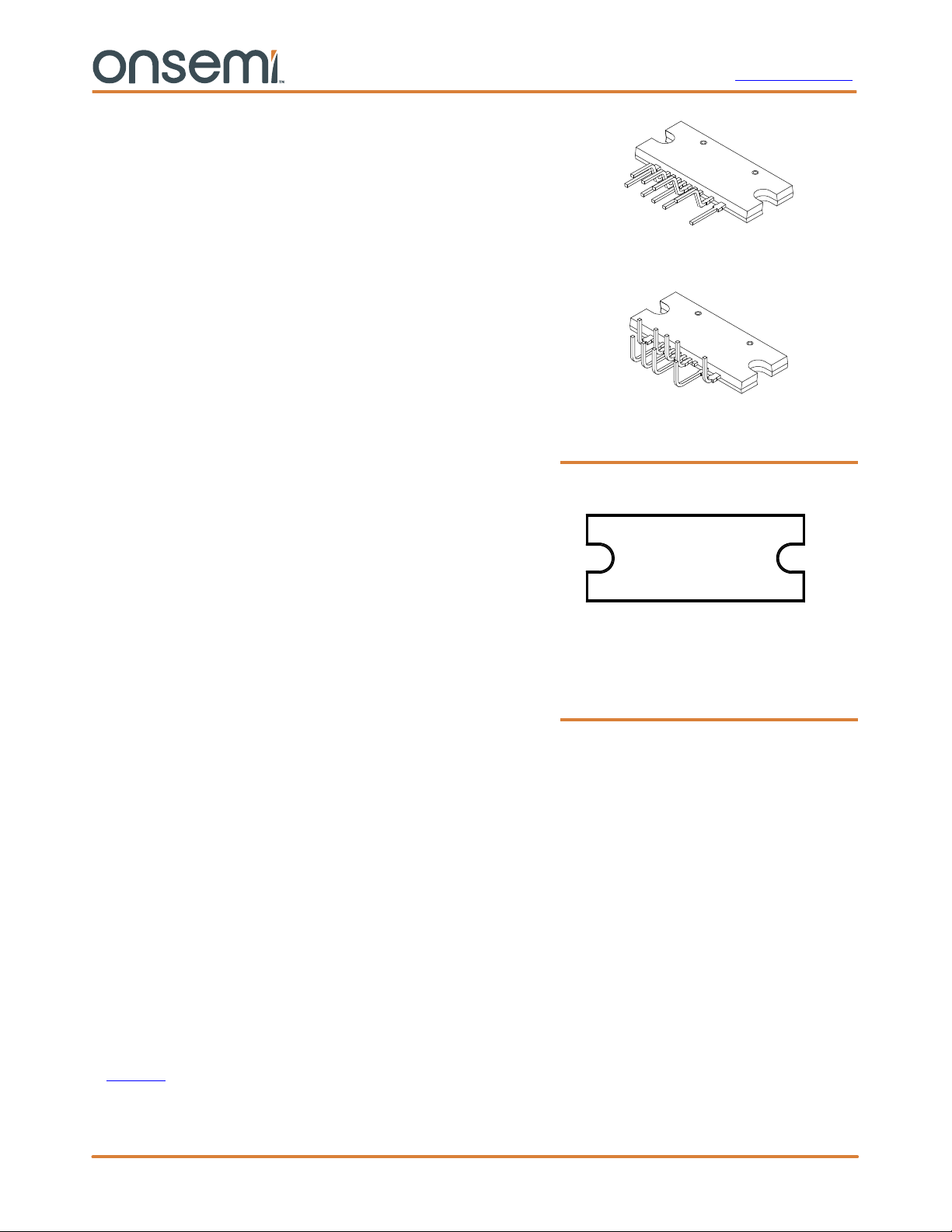
SIP9 26x10.5
CASE 127EM
SIP9 26x10.5
CASE 127EN
MARKING DIAGRAM
$Y&Z &3&K
XXXXXXXXXX
$Y = onsemi Logo
&Z = Assembly Plant Code
&3 = 3−Digit Date Code
&K = 2−Digits Lot Run Traceability Code
XXXXXXXXXX= Device Code
ORDERING INFORMATION
See detailed ordering and shipping information on page 2 of
this data sheet.
Applications
• PDP and LCD TVs
• Desktop PCs and Servers
• Adapters
• Telecom Power Supplies
Related Resources
AN−4151 − Half−Bridge LLC Resonant Converter Design Using
FSFR−Series Power Switch
© Semiconductor Components Industries, LLC, 2010
January, 2022 − Rev. 2
1 Publication Order Number:
FSFR2100XS/D
Page 2
FSFR−XS Series
ORDERING INFORMATION
Operating
Junction
Part Number Package
FSFR2100XS
9−SIP −40 to +130°C
FSFR1800XS
FSFR1700XS
FSFR1600XS
FSFR2100XSL
FSFR1800XSL
9−SIP
L−Forming
FSFR1700XSL
FSFR1600XSL
Temperature
R
DS(ON_MAX)
0.51 W
0.95 W
1.25 W
1.55 W
0.51 W
0.95 W
1.25 W
1.55 W
1. The junction temperature can limit the maximum output power.
2. Maximum practical continuous power in an open−frame design at 50°C ambient.
APPLICATION CIRCUIT DIAGRAM
Maximum Output Power
= 350~400 V) (Note 1, 2)
(V
IN
without Heatsink
Power with Heatsink
(V
IN
180 W 400 W
120 W 260 W
100 W 200 W
80 W 160 W
180 W 400 W
120 W 260 W
100 W 200 W
80 W 160 W
Maximum Output
= 350~400 V) (Note 1, 2)
Cr
V
IN
V
CC
V
O
LV
R
MIN
R
MAX
R
SS
R
T
AR
C
SS
CS
SG
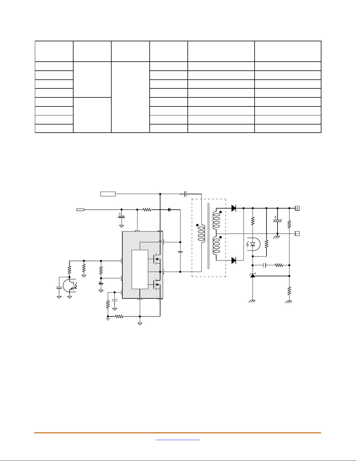
Figure 1. Typical Application Circuit (LLC Resonant Half−Bridge Converter)
CC
FSFR−XS
V
Series
PG
DL
HV
CC
V
CTR
www.onsemi.com
2
Page 3
FSFR−XS Series
BLOCK DIAGRAM
AR
LV
CC
V
REF
I
RT
V
REF
I
RT
2I
RT
3 V
1 V
S
Q
R
2 V
3
R
T
7
LUV+ / LUV−
LV
Time
Delay
CC
good
Internal
V
REF
Bias
HUV+ / HUV−
Level
Shifter
High−Side
Gate Driver
350 ns
V
DL
1
9
HV
CC
10
V
CTR
Divider
2
V
/ V
CssH
5 k
CssL
LVCC good
Time
Delay
350 ns
S
R
Q
Balancing
Delay
Shutdown
Low−Side
Gate Driver
TSD
V
LV
CC
V
OVP
Delay
50 ns
Delay
1.5 ms
AOCP
6
V
OCP
−1
PG
5
SG
4
CS
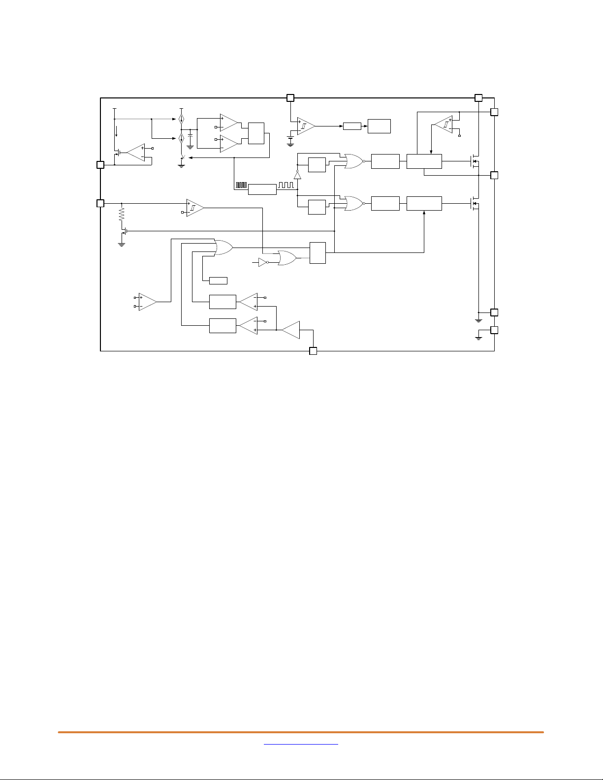
Figure 2. Internal Block Diagram
www.onsemi.com
3
Page 4
FSFR−XS Series
PIN CONFIGURATION
1
234567 9 108
V
DL
R
T
AR
CSSGPG
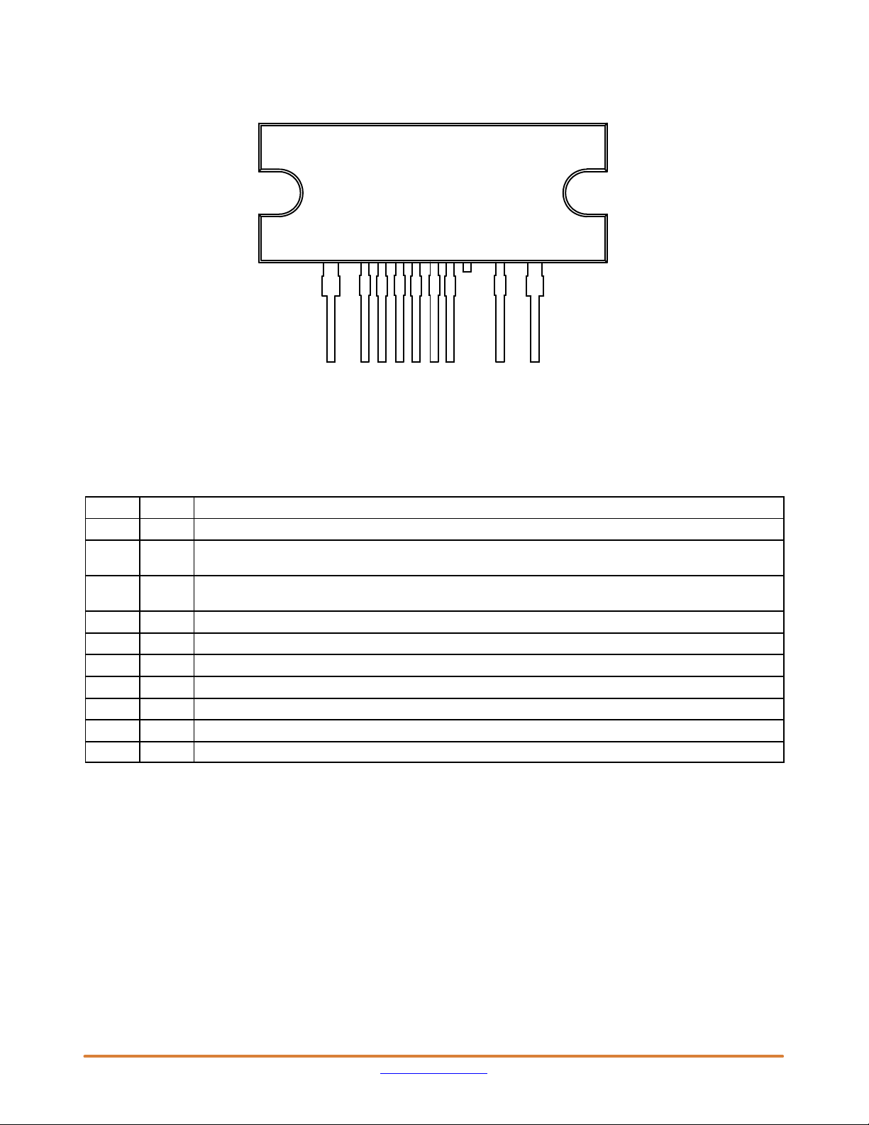
Figure 3. Package Diagram
LVcc
V
HVcc
PIN DESCRIPTION
Pin # Name Description
1 V
2 AR This pin is for discharging the external soft−start capacitor when any protections are triggered. When the voltage of
3 R
4 CS This pin senses the current flowing through the low−side MOSFET. Typically, negative voltage is applied on this pin.
5 SG This pin is the control ground.
6 PG This pin is the power ground. This pin is connected to the source of the low−side MOSFET.
7 LV
8 NC No connection.
9 HV
10 V
This is the drain of the high−side MOSFET, typically connected to the input DC link voltage.
DL
this pin drops to 0.2 V, all protections are reset and the controller starts to operate again.
This pin programs the switching frequency. Typically, an opto−coupler is connected to control the switching
T
frequency for the output voltage regulation.
This pin is the supply voltage of the control IC.
CC
This is the supply voltage of the high−side gate−drive circuit IC.
CC
This is the drain of the low−side MOSFET. Typically, a transformer is connected to this pin.
CTR
www.onsemi.com
4
Page 5
FSFR−XS Series
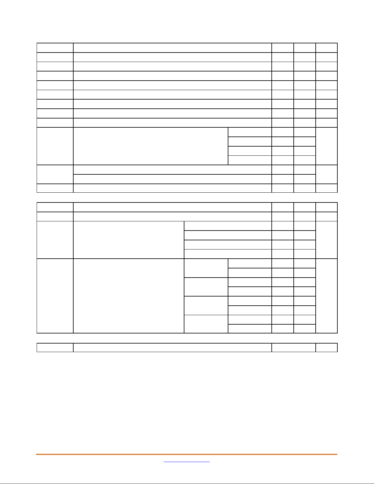
ABSOLUTE MAXIMUM RATINGS (T
Symbol
HV
CC
dV
V
LV
HV
V
V
V
DS
to V
AR
CS
RT
CTR
P
CC
CC
D
Maximum Drain−to−Source Voltage (VDL−V
Low−Side Supply Voltage −0.3 25.0 V
High−Side VCC Pin to Low−Side Drain Voltage −0.3 25.0 V
CTR
High−Side Floating Supply Voltage −0.3 525.0 V
Auto−Restart Pin Input Voltage −0.3 LV
Current−Sense (CS) Pin Input Voltage −5.0 1.0 V
RT Pin Input Voltage −0.3 5.0 V
/dt Allowable Low−Side MOSFET Drain Voltage Slew Rate − 50 V/ns
Total Power Dissipation (Note 3)
= 25°C unless otherwise specified)
A
Parameter Min Max Unit
and V
CTR
CTR
−PG) 500 − V
CC
FSFR2100XS/L − 12.0
V
W
FSFR1800XS/L − 11.7
FSFR1700XS/L − 11.6
FSFR1600XS/L − 11.5
°C
T
T
J
STG
Maximum Junction Temperature (Note 4) − +150
Recommended Operating Junction Temperature (Note 4) −40 +130
Storage Temperature Range −55 +150 °C
MOSFET SECTION
V
DGR
V
I
DM
GS
Drain Gate Voltage (R
GS
= 1 MW)
Gate Source (GND) Voltage − ±30 V
Drain Current Pulsed (Note 5)
FSFR2100XS/L − 32
500 − V
A
FSFR1800XS/L − 23
FSFR1700XS/L − 20
FSFR1600XS/L − 18
I
D
Continuous Drain Current FSFR2100XS/L
FSFR1800XS/L
FSFR1700XS/L
FSFR1600XS/L
T
= 25°C − 10.5
C
T
= 100°C − 6.5
C
T
= 25°C − 7.0
C
T
= 100°C − 4.5
C
T
= 25°C − 6.0
C
T
= 100°C − 3.9
C
T
= 25°C − 4.5
C
T
= 100°C − 2.7
C
A
PACKAGE SECTION
Torque
Recommended Screw Torque 5~7 kgf·cm
Stresses exceeding those listed in the Maximum Ratings table may damage the device. If any of these limits are exceeded, device functionality
should not be assumed, damage may occur and reliability may be affected.
3. Per MOSFET when both MOSFETs are conducting.
4. The maximum value of the recommended operating junction temperature is limited by thermal shutdown.
5. Pulse width is limited by maximum junction temperature.
www.onsemi.com
5
Page 6
FSFR−XS Series
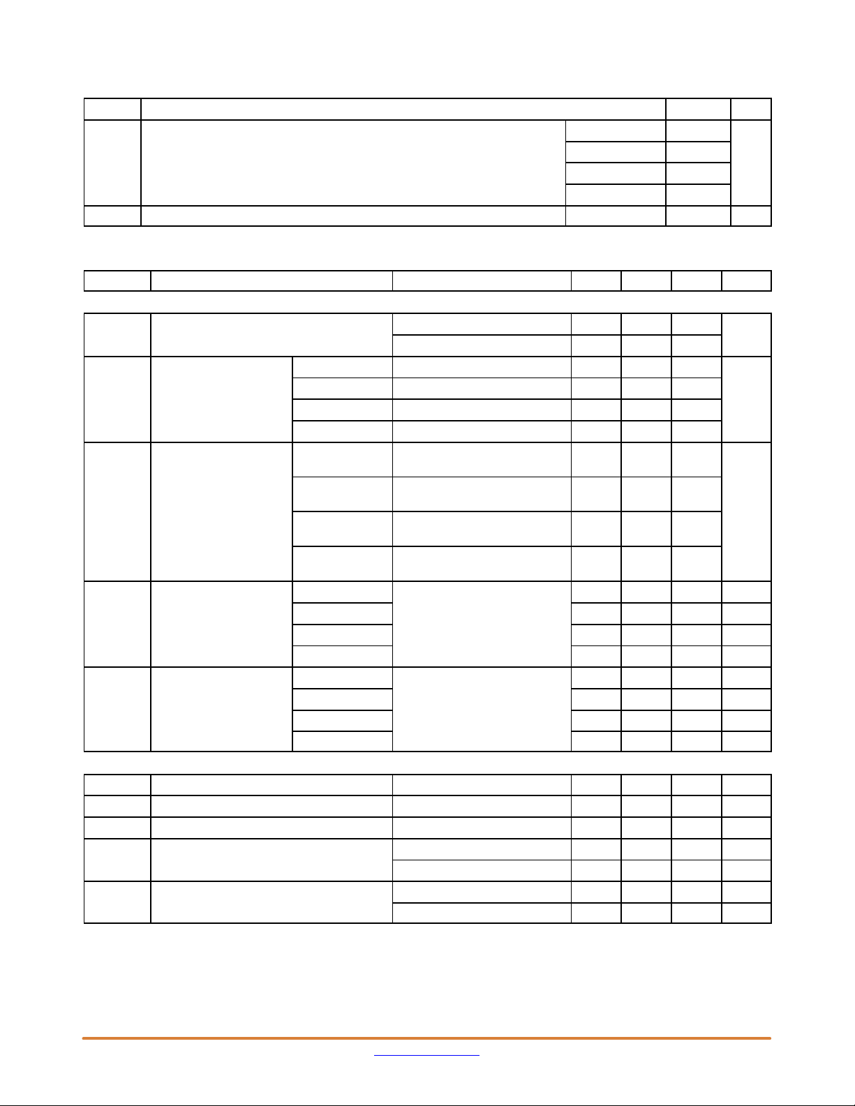
THERMAL IMPEDANCE (T
Symbol
q
Junction−to−Case Center Thermal Impedance (Both MOSFETs Conducting)
JC
= 25°C unless otherwise specified)
A
Parameter Value Unit
FSFR2100XS/L 10.44
FSFR1800XS/L 10.68
FSFR1700XS/L 10.79
FSFR1600XS/L 10.89
q
ELECTRICAL CHARACTERISTICS (T
Junction−to−Ambient Thermal Impedance FSFR XS Series 80 °C/W
JA
= 25°C unless otherwise noted)
A
Symbol Parameter Test Condition Min Ty p Max Unit
MOSFET SECTION
BV
R
DS(ON)
DSS
Drain−to−Source Breakdown Voltage
On−State Resistance
FSFR2100XS/L VGS = 10 V, ID = 6.0 A − 0.41 0.51 W
ID = 200 mA, TA = 25°C
ID = 200 mA, TA = 125°C
500 − −
− 540 −
FSFR1800XS/L VGS = 10 V, ID = 3.0 A − 0.77 0.95
FSFR1700XS/L VGS = 10 V, ID = 2.0 A − 1.00 1.25
FSFR1600XS/L VGS = 10 V, ID = 2.25 A − 1.25 1.55
t
rr
C
ISS
Body Diode Reverse
Recovery Time (Note 6)
Input Capacitance
(Note 6)
FSFR2100XS/L VGS = 0 V, I
/dt = 100A/ms
dI
Diode
FSFR1800XS/L VGS = 0 V, I
/dt = 100 A/ms
dI
Diode
FSFR1700XS/L VGS = 0 V, I
/dt = 100 A/ms
dI
Diode
FSFR1600XS/L VGS = 0 V, I
/dt = 100 A/ms
dI
Diode
FSFR2100XS/L
FSFR1800XS/L − 639 − pF
VDS = 25 V, VGS = 0 V,
f = 1.0 MHz
Diode
Diode
Diode
Diode
= 10.5 A,
= 7.0 A,
= 6.0 A,
= 4.5 A,
− 120 −
− 160 −
− 160 −
− 90 −
− 1175 − pF
FSFR1700XS/L − 512 − pF
FSFR1600XS/L − 412 − pF
C
OSS
Output Capacitance
(Note 6)
FSFR2100XS/L
FSFR1800XS/L − 82.1 − pF
VDS = 25 V, VGS = 0 V,
f = 1.0 MHz
− 155 − pF
FSFR1700XS/L − 66.5 − pF
FSFR1600XS/L − 52.7 − pF
SUPPLY SECTION
I
IQHV
IQLV
IOHV
LK
Offset Supply Leakage Current HVCC = V
Quiescent HVCC Supply Current (HVCCUV+) − 0.1 V − 50 120
CC
Quiescent LVCC Supply Current (LVCCUV+) − 0.1 V − 100 200
CC
Operating HVCC Supply Current (RMS Value)
CC
f
= 100 kHz − 6 9 mA
OSC
= 500 V − − 50
CTR
No Switching − 100 200
IOLV
Operating LVCC Supply Current (RMS Value)
CC
f
= 100 kHz − 7 11 mA
OSC
No Switching − 2 4 mA
°C/W
V
ns
mA
mA
mA
mA
www.onsemi.com
6
Page 7
FSFR−XS Series
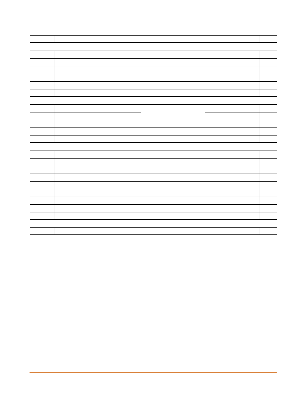
ELECTRICAL CHARACTERISTICS (T
= 25°C unless otherwise noted) (continued)
A
Symbol UnitMaxTypMinTest ConditionParameter
UVLO SECTION
UV+ LVCC Supply Under−Voltage Positive Going Threshold (LVCC Start) 11.2 12.5 13.8 V
LV
CC
LVCCUV− LVCC Supply Under−Voltage Negative Going Threshold (LVCC Stop) 8.9 10.0 11.1 V
LVCCUVH LVCC Supply Under−Voltage Hysteresis − 2.50 − V
HVCCUV+ HVCC Supply Under−Voltage Positive Going Threshold (HVCC Start) 8.2 9.2 10.2 V
HVCCUV− HVCC Supply Under−Voltage Negative Going Threshold (HVCC Stop) 7.8 8.7 9.6 V
HVCCUVH HVCC Supply Under−Voltage Hysteresis − 0.5 − V
OSCILLATOR & FEEDBACK SECTION
V
f
OSC
RT
V−I Converter Threshold Voltage RT = 5.2 kW 1.5 2.0 2.5 V
Output Oscillation Frequency 94 100 106 kHz
DC Output Duty Cycle 48 50 52 %
f
SS
t
SS
Internal Soft−Start Initial Frequency
fSS = f
+ 40 kHz, RT = 5.2 kW
OSC
− 140 − kHz
Internal Soft−Start Time 2 3 4 ms
PROTECTION SECTION
V
V
V
V
AOCP
t
V
T
CssH
CssL
OVP
BAO
OCP
t
BO
t
DA
SD
Beginning Voltage to Discharge C
SS
Beginning Voltage to Charge CSS and Restart 0.16 0.20 0.24 V
LVCC Over−Voltage Protection LVCC > 21 V 21 23 25 V
AOCP Threshold Voltage −1.0 −0.9 −0.8 V
AOCP Blanking Time (Note 6) V
CS
< V
AOCP
OCP Threshold Voltage −0.64 −0.58 −0.52 V
OCP Blanking Time (Note 6) V
Delay Time (Low Side) Detecting from V
AOCP
< V
CS
OCP
to Switch Off (Note 6) − 250 400 ns
Thermal Shutdown Temperature (Note 6) 120 135 150 °C
0.9 1.0 1.1 V
− 50 − ns
1.0 1.5 2.0
ms
DEAD−TIME CONTROL SECTION
D
Dead Time (Note 7) − 350 − ns
T
Product parametric performance is indicated in the Electrical Characteristics for the listed test conditions, unless otherwise noted. Product
performance may not be indicated by the Electrical Characteristics if operated under different conditions.
6. This parameter, although guaranteed, is not tested in production.
7. These parameters, although guaranteed, are tested only in EDS (wafer test) process.
www.onsemi.com
7
Page 8
FSFR−XS Series
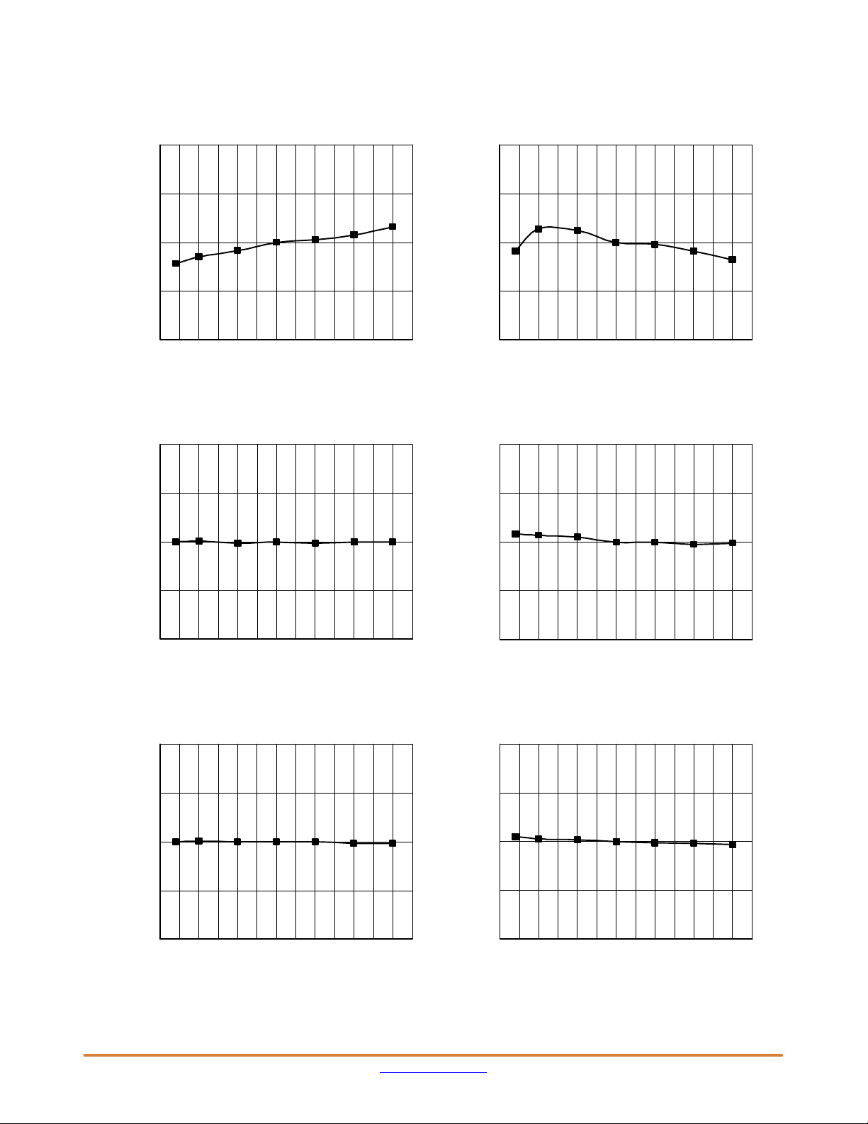
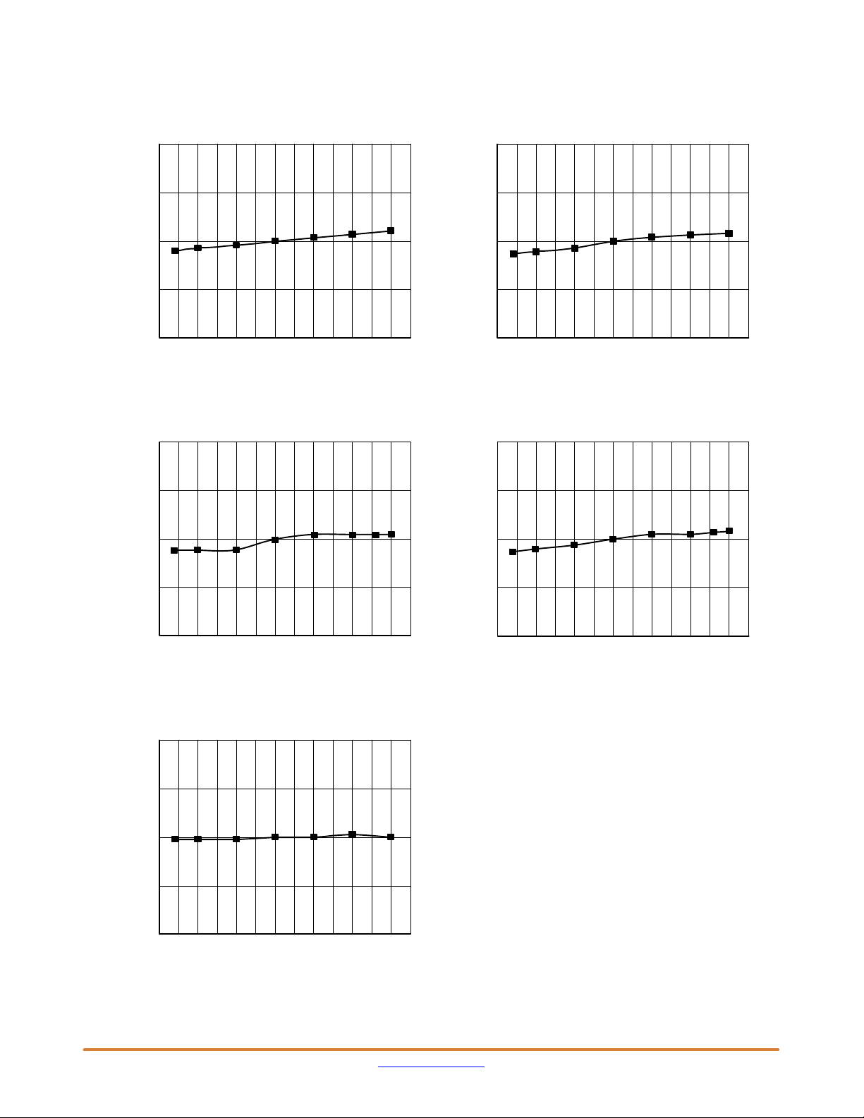
TYPICAL PERFORMANCE CHARACTERISTICS
(These characteristic graphs are normalized at TA = 25°C)
1.1
1.05
1
0.95
0.9
−50 −25 0 25 50 75 100
Temp (°C) Temp (°C)
Figure 4. Low−Side MOSFET Duty Cycle vs.
Temperature
1.1
1.05
1
1.1
1.05
1
Normalized at 25°C
0.95
0.9
−50 −25 0 25 50 75 100
Figure 5. Switching Frequency vs. Temperature
1.1
1.05
1
Normalized at 25°C Normalized at 25°C
0.95
0.9
−50 −250255075100
Temp (°C) Temp (°C)
Figure 6. High−Side V
(HVCC) Start vs.
CC
Temperature
1.1
1.05
1
Normalized at 25°C
0.95
0.9
−50 −25 0 25 50 75 100
Temp (°C) Temp (°C)
Normalized at 25°C
0.95
0.9
−50 −25 0 25 50 75 100
Figure 7. High−Side VCC (HVCC) Stop vs.
Temperature
1.1
1.05
1
Normalized at 25°C
0.95
0.9
−50 −250 255075100
Figure 8. Low−Side V
Temperature
(LVCC) Start vs.
CC
Figure 9. Low−Side VCC (LVCC) Stop vs.
Temperature
www.onsemi.com
8
Page 9
FSFR−XS Series
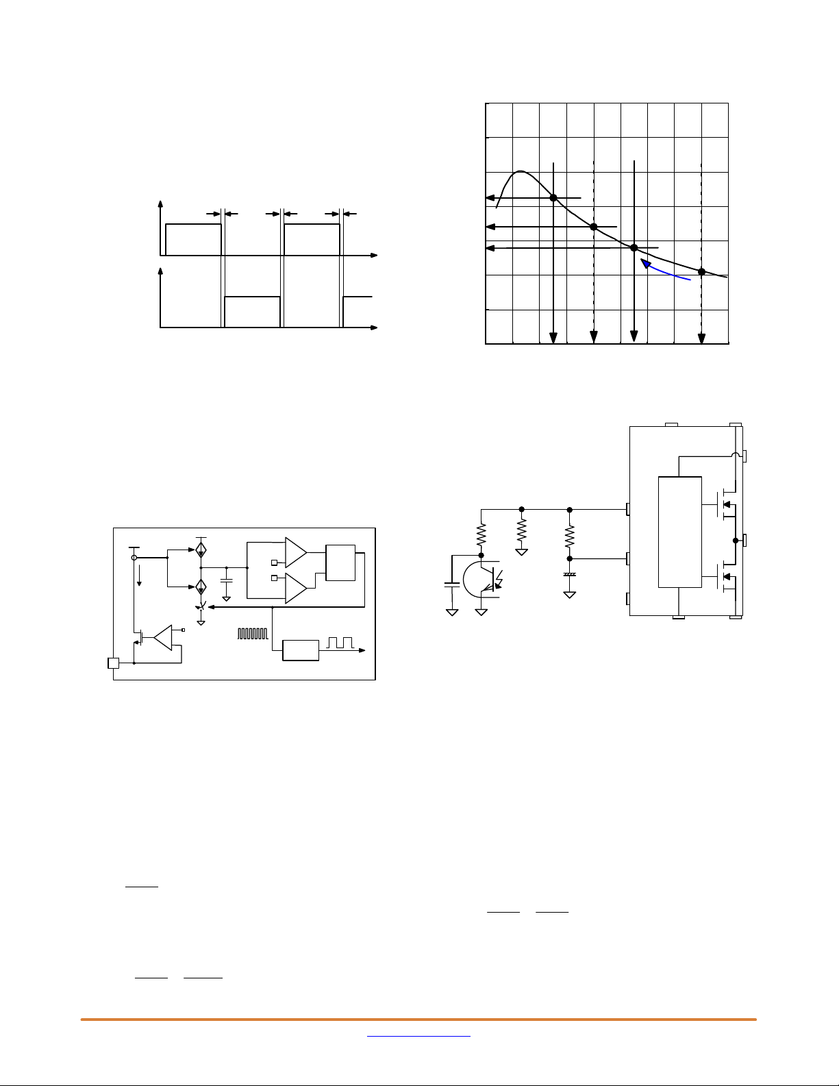
TYPICAL PERFORMANCE CHARACTERISTICS (continued)
(These characteristic graphs are normalized at T
= 25°C)
A
1.1
1.05
1
0.95
0.9
−50 −25 0 25 50 75 100
Temp (°C) Temp (°C)
Figure 10. LVCC OVP Voltage vs.
Temperature
1.1
1.05
1
1.1
1.05
1
Normalized at 25°C
0.95
0.9
−50 −25 0 25 50 75 100
Figure 11. RT Voltage vs. Temperature
1.1
1.05
1
Normalized at 25°C Normalized at 25°C
0.95
0.9
−50 −250255075100
Temp (°C) Temp (°C)
Figure 12. V
1.1
1.05
1
Normalized at 25°C
0.95
0.9
−50 −25 0 25 50 75 100
vs. Temperature Figure 13. V
CssL
Temp (°C)
Normalized at 25°C
0.95
0.9
−50 −25 0 25 50 75 100
vs. Temperature
CssH
Figure 14. OCP Voltage vs. Temperature
www.onsemi.com
9
Page 10
FSFR−XS Series
FUNCTIONAL DESCRIPTION
Basic Operation
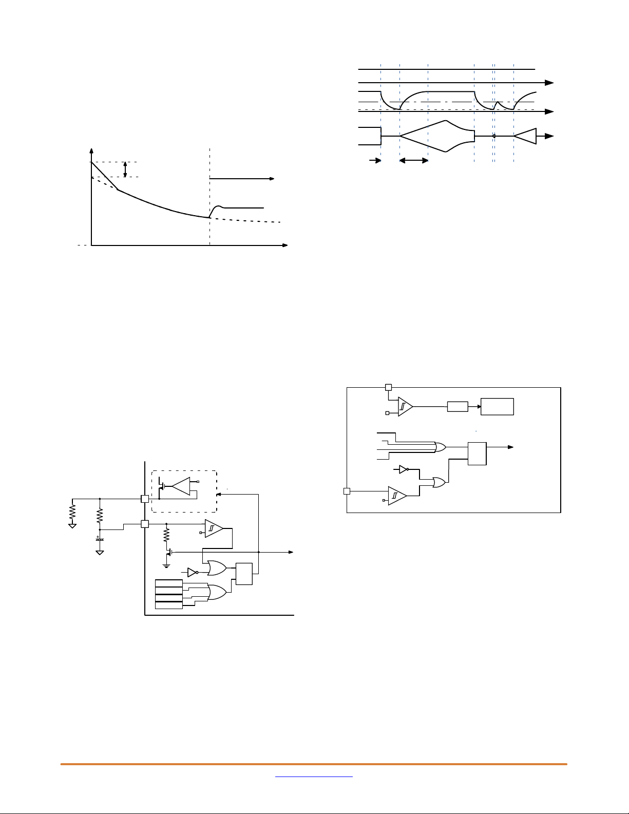
FSFR−XS series is designed to drive high−side and
low−side MOSFETs complementarily with 50% duty cycle.
A fixed dead time of 350 ns is introduced between
consecutive transitions, as shown in Figure 15.
Dead−Time
High−Side
MOSFET
Gate Drive
Low−Side
MOSFET
Gate Drive
Time
Figure 15. MOSFETs Gate Drive Signal
Internal Oscillator
FSFR−XS series employs a current−controlled oscillator,
as shown in Figure 16. Internally, the voltage of R
pin is
T
regulated at 2 V and the charging / discharging current for
the oscillator capacitor, C
current flowing out of the R
mirror. Therefore, the switching frequency increases as I
, is obtained by copying the
T
pin (I
T
) using a current
CTC
CTC
increases.
V
I
REF
CTC
I
CTC
2I
CTC
C
T
3 V
1 V
+
−
+
−
S
−QQR
F/F
Gain
1.8
1.6
1.4
1.2
1.0
0.8
0.6
min
f
normal
f
Frequency (kHz)
max
f
Soft−Start
ISS
f
140 15060 70 80 90 100 110 120 130
Figure 17. Resonant Converter Typical Gain Curve
LV
R
T
R
max
R
min
R
ss
+
C
ss
AR
CS
CC
VDL
FSFR−XS
+
2 V
R
T
3
−
Divider
Gate Drive
Figure 16. Current−Controlled Oscillator
Frequency Setting
Figure 17 shows the typical voltage gain curve of a resonant
converter, where the gain is inversely proportional to the
switching frequency in the ZVS region. The output voltage
can be regulated by modulating the switching frequency.
Figure 18 shows the typical circuit configuration for the R
pin, where the opto−coupler transistor is connected to the R
pin to modulate the switching frequency.
The minimum switching frequency is determined as:
5.2 kW
min
f
+
R
min
100 (kHz)
(eq. 1)
Assuming the saturation voltage of opto−coupler
transistor is 0.2 V, the maximum switching frequency is
determined as:
f
max
5.2 kW
ǒ
+
R
min
4.68 kW
)
Ǔ
max
100 (kHz)
R
(eq. 2)
SG
Figure 18. Frequency Control Circuit
To prevent excessive inrush current and overshoot of
output voltage during startup, increase the voltage gain of
the resonant converter progressively. Since the voltage gain
of the resonant converter is inversely proportional to the
switching frequency, the soft−start is implemented by
sweeping down the switching frequency from an initial high
frequency (f
ISS
) until the output voltage is established. The
soft−start circuit is made by connecting R−C series network
T
on the R
T
has a 3 ms internal soft−start to reduce the current overshoot
pin, as shown in Figure 18. FSFR−XS series also
T
during the initial cycles, which adds 40 kHz to the initial
frequency of the external soft−start circuit, as shown in
Figure 19. The initial frequency of the soft−start is given as:
min
)
5.2 kW
R
SS
Ǔ
100 ) 40 (kHz)
5.2 kW
ISS
ǒ
f
+
R
PG
(eq. 3)
www.onsemi.com
10
Page 11
FSFR−XS Series
It is typical to set the initial frequency of soft−start two to
three times the resonant frequency (f
) of the resonant
O
network. The soft−start time is three to four times the RC
time constant. The RC time constant is:
t + RSS@ C
ISS
f
Figure 19. Frequency Sweeping of Soft−Start
Self Auto−Restart
SS
f
s
(eq. 4)
40 kHz
Control Loop
Take Over
Time
The FSFR−XS series can restart automatically even
though any built−in protections are triggered with external
supply voltage. As can be seen in Figure 20 and Figure 21,
once any protections are triggered, the M1 switch turns on
and the V−I converter is disabled. C
until V
across CSS drops to V
Css
starts to discharge
SS
. Then, all protections
CssL
are reset, M1 turns off, and the V−I converter resumes at the
same time. The FSFR−XS starts switching again with
soft−start. If the protections occur while V
and V
V
Css
level, the switching is terminated immediately,
CssH
continues to increase until reaching V
is under V
Css
CssH
CssL
, then CSS is
discharged by M1.
+
2 V
+
−
‘H’ = disable
R
Q
S
Switching
Shutdown
V−I Converter
V
/ V
good
CC
OVP
OCP
AOCP
TSD
−
CssH
CssL
R
T
3
R
min
R
AR
ss
2
C
ss
5k
M1
LV
Figure 20. Internal Block of AR Pin
After protections trigger, FSFR−XS is disabled during the
stop−time, t
, where V
stop
decreases and reaches to V
Css
CssL
The stop−time of FSFR−XS can be estimated as:
t
+ CSS@ {(RSS) R
STOP
The soft−start time, t
) ø 5kW}
MIN
can be set as Equation (4).
s/s
(eq. 5)
LV
(a) (a)(b)
CC
V
AR
I
Cr
t
stoptS/S
(b)(a) (b)
(a) Protections are triggered, (b) FSFR−US restarts
Figure 21. Self Auto−Restart Operation
Protection Circuits
The FSFR−XS series has several self−protective
functions, such as Over−Current Protection (OCP),
Abnormal Over−Current Protection (AOCP), Over−Voltage
Protection (OVP), and Thermal Shutdown (TSD). These
protections are auto−restart mode protections, as shown in
Figure 22.
Once a fault condition is detected, switching is terminated
and the MOSFETs remain off. When LV
falls to the LV
CC
stop voltage of 10 V or AR signal is HIGH, the protection is
reset. The FSFR−XS resumes normal operation when LV
reaches the start voltage of 12.5 V.
LV
CC
7
+
LV
good
AR
10 / 12.5 V
2
V
CssH
OCP
AOCP
OVP
TSD
LVCC good
/ V
CssL
+
−
−
AR Signal
CC
V
REF
Auto−Restart
Protection
S
−QQR
F/F
Internal
Bias
Figure 22. Protection Blocks
Over−Current Protection (OCP)
When the sensing pin voltage drops below −0.58 V, OCP
is triggered and the MOSFETs remain off. This protection
has a shutdown time delay of 1.5 ms to prevent premature
shutdown during startup.
Abnormal Over−Current Protection (AOCP)
If the secondary rectifier diodes are shorted, large current
with extremely high di/dt can flow through the MOSFET
before OCP is triggered. AOCP is triggered without
shutdown delay if the sensing pin voltage drops below
.
−0.9 V.
Over−Voltage Protection (OVP)
When the LV
reaches 23 V, OVP is triggered. This
CC
protection is used when auxiliary winding of the transformer
to supply V
to the power switch is utilized.
CC
V
V
Switching
Shutdown
CssH
CssL
CC
CC
www.onsemi.com
11
Page 12
FSFR−XS Series
Thermal Shutdown (TSD)
The MOSFETs and the control IC in one package makes
it easier for the control IC to detect the abnormal
over−temperature of the MOSFETs. If the temperature
exceeds approximately 130°C, thermal shutdown triggers.
Current Sensing Using a Resistor
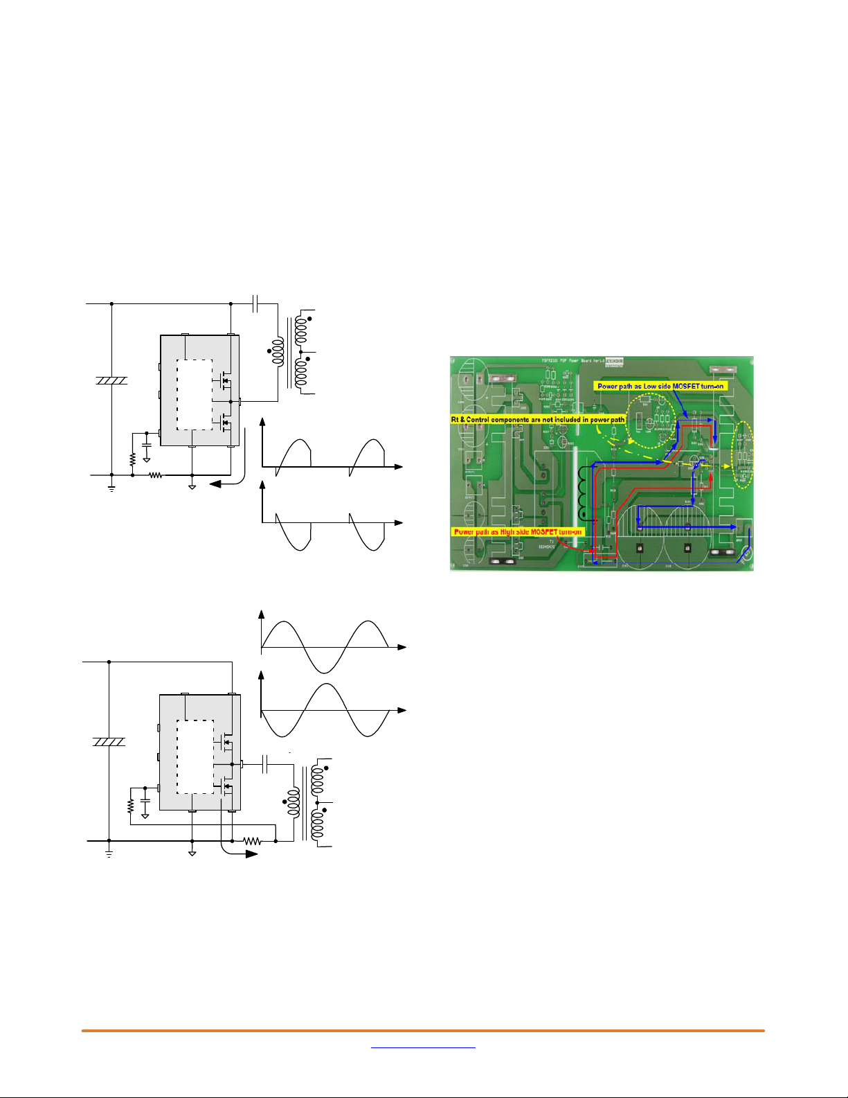
FSFR−XS series senses drain current as a negative
voltage, as shown in Figure 23 and Figure 24. Half−wave
sensing allows low power dissipation in the sensing resistor,
while full−wave sensing has less switching noise in the
sensing signal.
Cr
Np
+
Control
V
CS
IC
CS
SG
R
sense
+−
PG
Ids
Ns
Ns
I
ds
V
CS
PCB Layout Guidelines
Duty imbalance problems may occur due to the radiated
noise from the main transformer, the inequality of the
secondary side leakage inductances of main transformer,
and so on. This is one of the reasons that the control
components in the vicinity of R
pin are enclosed by the
T
primary current flow pattern on PCB layout. The direction
of the magnetic field on the components caused by the
primary current flow is changed when the high− and
low−side MOSFET turn on by turns. The magnetic fields
with opposite directions induce a current through, into, or
out of the R
pin, which makes the turn−on duration of each
T
MOSFET different. It is strongly recommended to separate
the control components in the vicinity of R
pin from the
T
primary current flow pattern on PCB layout. Figure 25
shows an example for the duty−balanced case.
Figure 23. Half−Wave Sensing
Figure 25. Example for Duty Balancing
I
ds
V
CS
+
PG
R
sense
+ −
Cr
Np
Ns
Ns
Control
V
CS
IC
CS
SG
Ids
Figure 24. Full−Wave Sensing
UniFET is trademark of Semiconductor Components Industries, LLC dba “onsemi” or its affiliates and/or subsidiaries in the United States and/or other
countries.
www.onsemi.com
12
Page 13
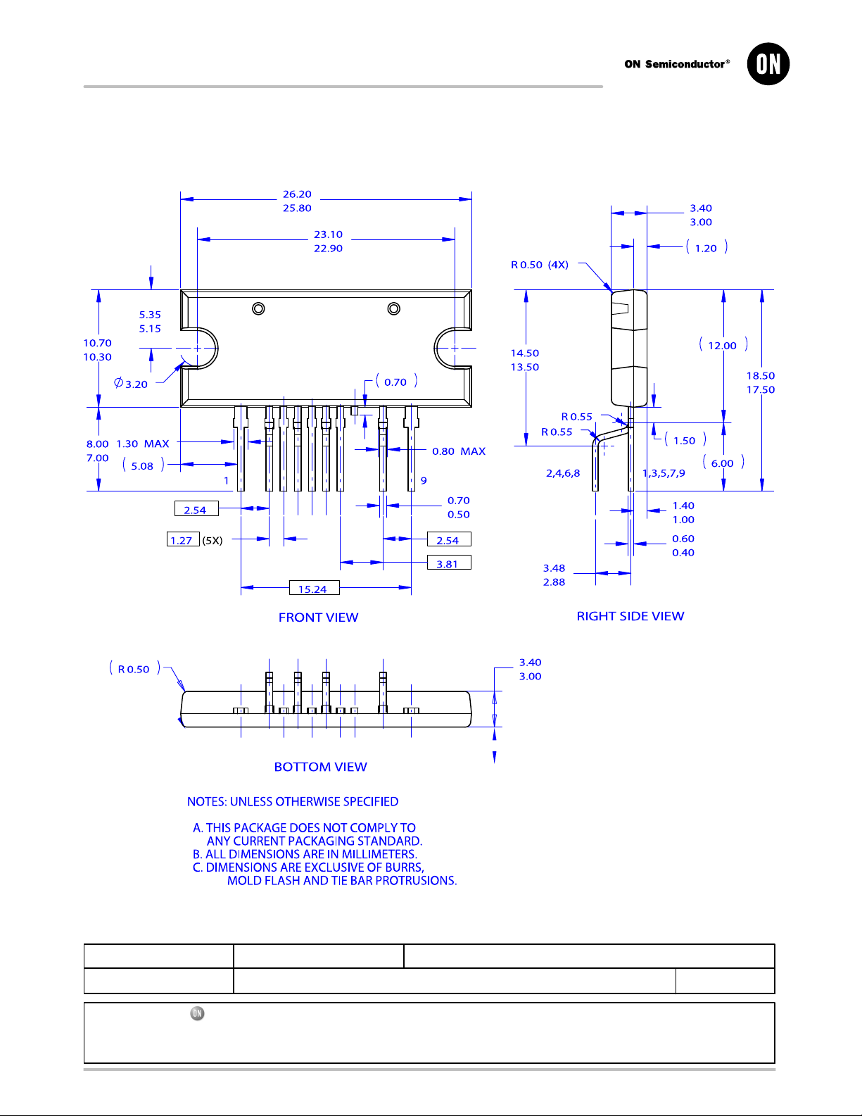
MECHANICAL CASE OUTLINE
PACKAGE DIMENSIONS
SIP9 26x10.5
CASE 127EM
ISSUE O
DATE 31 DEC 2016
DOCUMENT NUMBER:
DESCRIPTION:
ON Semiconductor and are trademarks of Semiconductor Components Industries, LLC dba ON Semiconductor or its subsidiaries in the United States and/or other countries.
ON Semiconductor reserves the right to make changes without further notice to any products herein. ON Semiconductor makes no warranty, representation or guarantee regarding
the suitability of its products for any particular purpose, nor does ON Semiconductor assume any liability arising out of the application or use of any product or circuit, and specifically
disclaims any and all liability, including without limitation special, consequential or incidental damages. ON Semiconductor does not convey any license under its patent rights nor the
rights of others.
© Semiconductor Components Industries, LLC, 2019
98AON13718G
SIP9 26x10.5
Electronic versions are uncontrolled except when accessed directly from the Document Repository.
Printed versions are uncontrolled except when stamped “CONTROLLED COPY” in red.
PAGE 1 OF 1
www.onsemi.com
Page 14
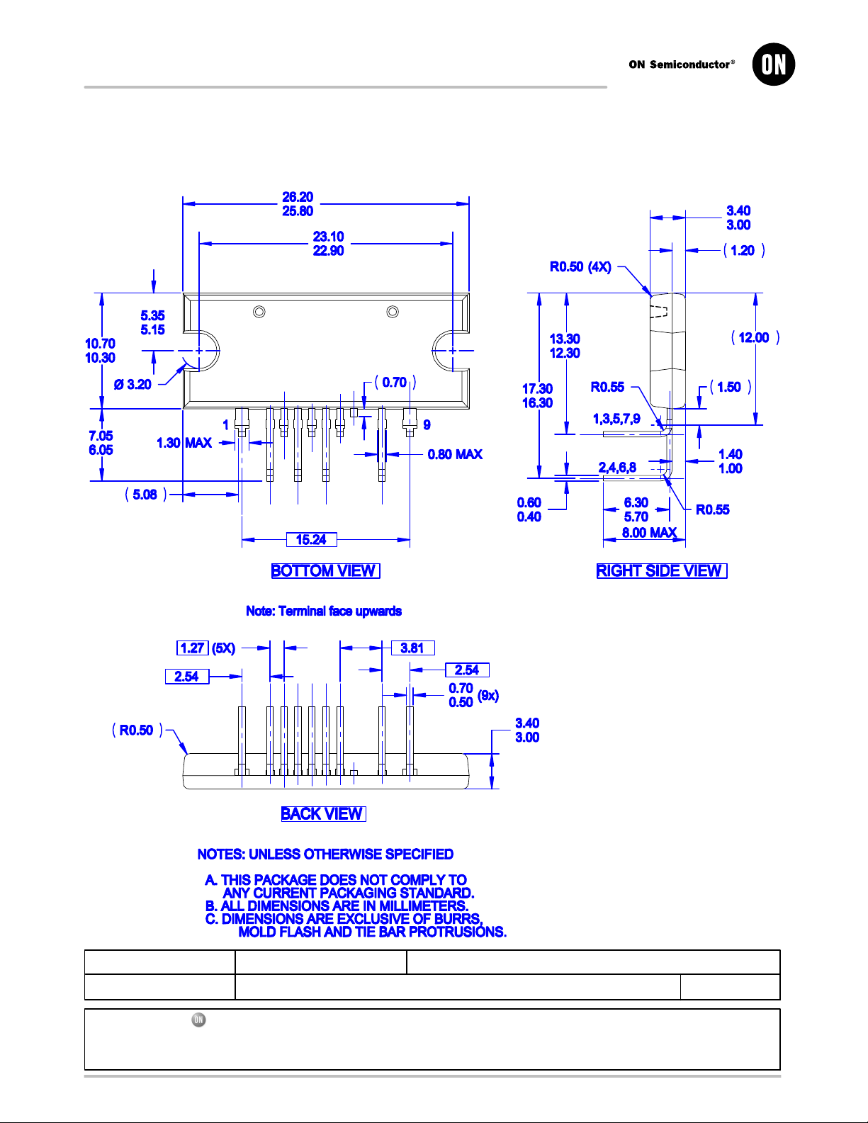
MECHANICAL CASE OUTLINE
PACKAGE DIMENSIONS
SIP9 26x10.5
CASE 127EN
ISSUE O
DATE 31 DEC 2016
DOCUMENT NUMBER:
DESCRIPTION:
ON Semiconductor and are trademarks of Semiconductor Components Industries, LLC dba ON Semiconductor or its subsidiaries in the United States and/or other countries.
ON Semiconductor reserves the right to make changes without further notice to any products herein. ON Semiconductor makes no warranty, representation or guarantee regarding
the suitability of its products for any particular purpose, nor does ON Semiconductor assume any liability arising out of the application or use of any product or circuit, and specifically
disclaims any and all liability, including without limitation special, consequential or incidental damages. ON Semiconductor does not convey any license under its patent rights nor the
rights of others.
© Semiconductor Components Industries, LLC, 2019
98AON13719G
SIP9 26x10.5
Electronic versions are uncontrolled except when accessed directly from the Document Repository.
Printed versions are uncontrolled except when stamped “CONTROLLED COPY” in red.
PAGE 1 OF 1
www.onsemi.com
Page 15

onsemi, , and other names, marks, and brands are registered and/or common law trademarks of Semiconductor Components Industries, LLC dba “onsemi” or its affiliates
and/or subsidiaries in the United States and/or other countries. onsemi owns the rights to a number of patents, trademarks, copyrights, trade secrets, and other intellectual property.
A listing of onsemi’s product/patent coverage may be accessed at www.onsemi.com/site/pdf/Patent−Marking.pdf
products or information herein, without notice. The information herein is provided “as−is” and onsemi makes no warranty, representation or guarantee regarding the accuracy of the
information, product features, availability, functionality, or suitability of its products for any particular purpose, nor does onsemi assume any liability arising out of the application or use
of any product or circuit, and specifically disclaims any and all liability, including without limitation special, consequential or incidental damages. Buyer is responsible for its products
and applications using onsemi products, including compliance with all laws, regulations and safety requirements or standards, regardless of any support or applications information
provided by onsemi. “Typical” parameters which may be provided in onsemi data sheets and/or specifications can and do vary in different applications and actual performance may
vary over time. All operating parameters, including “Typicals” must be validated for each customer application by customer’s technical experts. onsemi does not convey any license
under any of its intellectual property rights nor the rights of others. onsemi products are not designed, intended, or authorized for use as a critical component in life support systems
or any FDA Class 3 medical devices or medical devices with a same or similar classification in a foreign jurisdiction or any devices intended for implantation in the human body. Should
Buyer purchase or use onsemi products for any such unintended or unauthorized application, Buyer shall indemnify and hold onsemi and its officers, employees, subsidiaries, affiliates,
and distributors harmless against all claims, costs, damages, and expenses, and reasonable attorney fees arising out of, directly or indirectly, any claim of personal injury or death
associated with such unintended or unauthorized use, even if such claim alleges that onsemi was negligent regarding the design or manufacture of the part. onsemi is an Equal
Opportunity/Affirmative Action Employer. This literature is subject to all applicable copyright laws and is not for resale in any manner.
. onsemi reserves the right to make changes at any time to any
ADDITIONAL INFORMATION
TECHNICAL PUBLICATIONS:
Technical Library: www.onsemi.com/design/resources/technical−documentation
onsemi Website: www.onsemi.com
ONLINE SUPPORT: www.onsemi.com/support
For additional information, please contact your local Sales Representative at
www.onsemi.com/support/sales
 Loading...