

Page 1
FSFA2100 — Fairchild Power Switch (FPS™)
for Half-Bridge PWM Converters
FSFA2100 — Fairchild Power Switch (FPS
September 2008
Features
Optimized for Complementary Driven Half-Bridge
Soft-Switching Converters
Can be Applied to Various Topologies: Asymmetric
PWM Half-Bridge Converters, Asymmetric PWM
Flyback Converters, Asymmetric PWM Forward
Converters, Active Clamp Flyback Converters
High Efficiency through Zero-Voltage-Switching (ZVS)
Internal SuperFET™s with Fast-Recovery Type
Body Diode (t
=120ns)
rr
Fixed Dead Time (200ns) Optimized for MOSFETs
Up to 300kHz Operating Frequency
Internal Soft-Start
Pulse-by-Pulse Current Limit
Burst-Mode Operation for Low Standby Power
Consumption
Protection Functions: Over-Voltage Protection
(OVP), Over-Load Protection (OLP), Abnormal
Over-Current Protection (AOCP), Internal Thermal
Shutdown (TSD)
Applications
PDP and LCD TVs
Desktop PCs and Servers
Adapters
Telecom Power Supplies
Description
The growing demand for higher power density and low
profile in power converter designs has forced designers
to increase switching frequencies. Operation at higher
frequencies considerably reduces the size of passive
components, such as transformers and filters. However,
switching losses have been an obstacle to highfrequency operation. To reduce switching losses and
allow high-frequency operation, Pulse Width Modulation
(PWM) with soft-switching techniques have been
developed. These techniques allow switching devices to
be softly commutated, which dramatically reduces the
switching losses and noise.
FSFA2100 is an integrated PWM controller and
SuperFET™ specifically designed for Zero-VoltageSwitching (ZVS) half-bridge converters with minimal
external components. The internal controller includes an
oscillator, under-voltage-lockout, leading-edge blanking
(LEB), optimized high-side and low-side gate driver,
internal soft-start, temperature-compensated precise
current sources for loop compensation and selfprotection circuitry. Compared with discrete MOSFET
and PWM controller solution, FSFA2100 can reduce total
cost; component count, size, and weight; while
simultaneously increasing efficiency, productivity, and
system reliability.
™
) for Half-Bridge PWM Converter
Ordering Information
Part
Number
FSFA2100
Notes:
1. The junction temperature can limit the maximum output power.
2. Maximum practical continuous power in an open-frame design at 50°C ambient.
For Fairchild’s definition of “green” Eco Status, please visit: http://www.fairchildsemi.com/company/green/rohs_green.html.
© 2008 Fairchild Semiconductor Corporation www.fairchildsemi.com
FSFA2100 • Rev. 1.0.0
Operating
Junction
Temperature
-40 to +130°C
R
DS(ON_MAX)
0.38Ω
Maximum Output
Power without
Heatsink
=350~400V)
(V
IN
200W 450W 9-SIP
(1,2)
Maximum Output
Power with Heatsink
=350~400V)
(V
IN
(1,2)
Package
Eco
Status
RoHS
Page 2
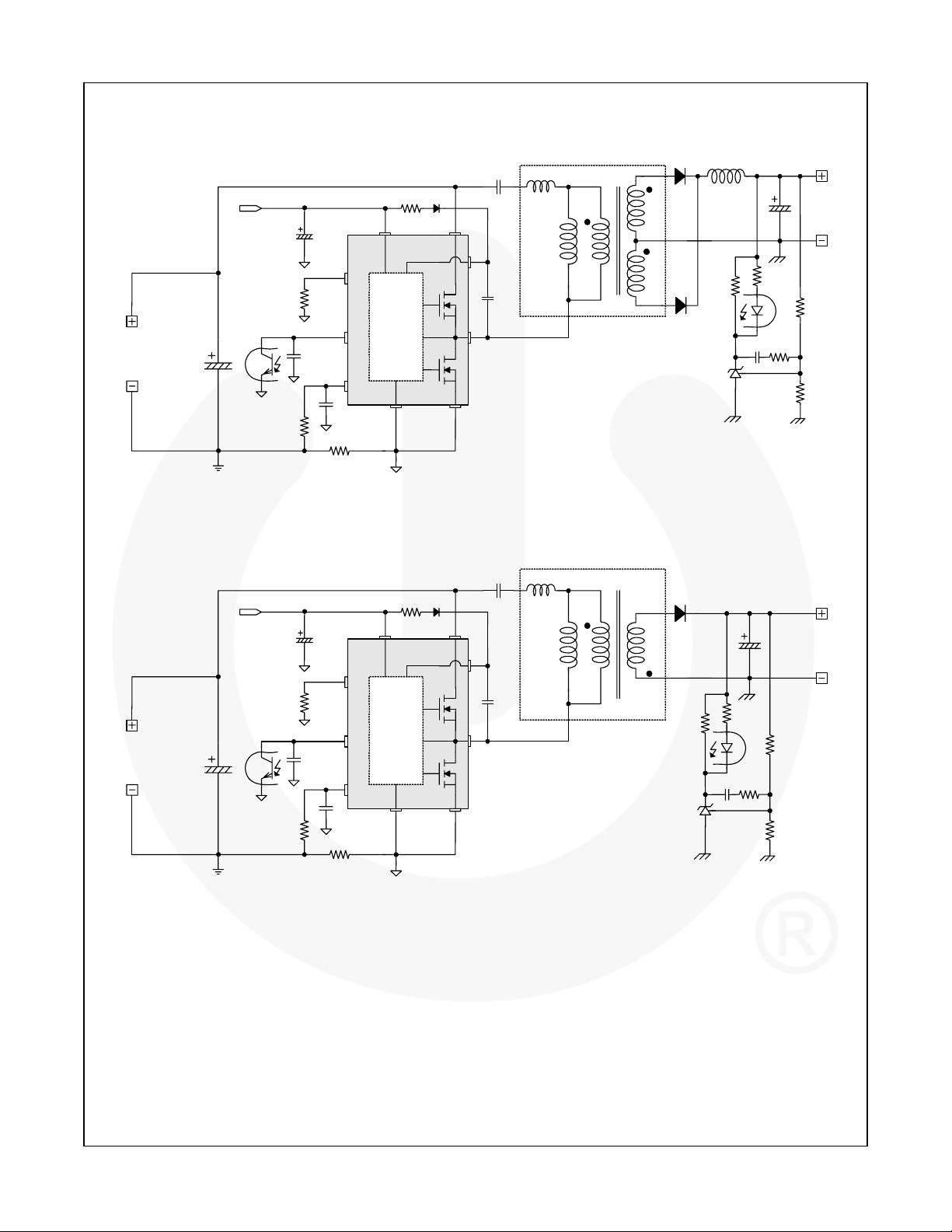
Application Circuit Diagram
FSFA2100 — Fairchild Power Switch (FPS™) for Half-Bridge PWM Converter
Ns
Ns
D1
D2
KA431
V
O
R
C
F
F
C
B
L
lk
Np
V
CC
C
DL
V
IN
LVcc
R
T
V
Control
FB
V
DL
Lm
HVcc
IC
V
CTR
CS
SG PG
R
sense
Figure 1. Typical Application Circuit for an Asymmetric PWM Half-Bridge Converter
C
B
Ns
D1
V
O
L
lk
Np
V
CC
LVcc
R
T
V
DL
Lm
HVcc
FB
sense
Control
IC
SG PG
V
CTR
R
C
F
F
KA431
C
DL
V
IN
V
CS
R
Figure 2. Typical Application Circuit for an Asymmetric PWM Flyback Converter
© 2008 Fairchild Semiconductor Corporation www.fairchildsemi.com
FSFA2100 • Rev. 1.0.0 2
Page 3
Block Diagram
FSFA2100 — Fairchild Power Switch (FPS™) for Half-Bridge PWM Converter
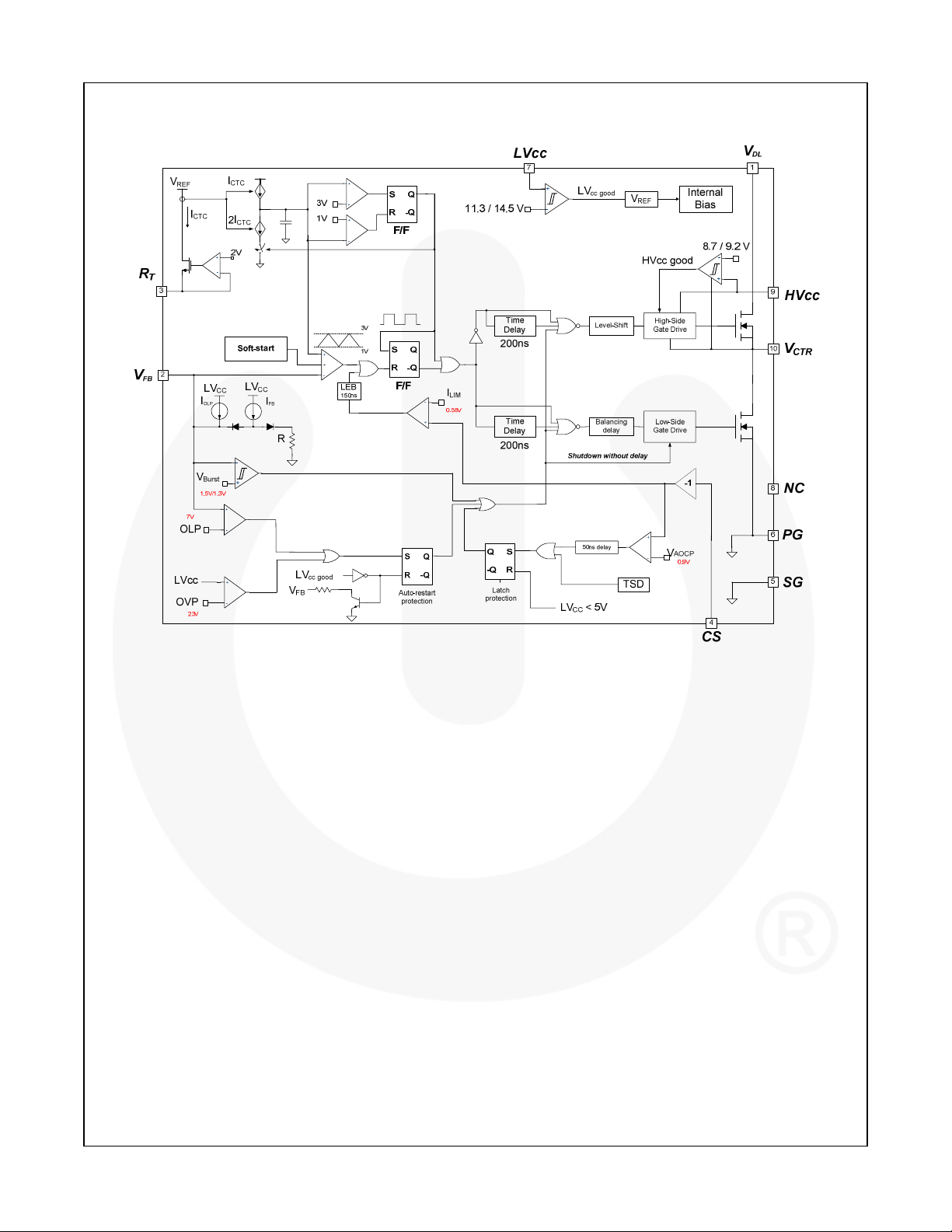
Figure 3. Internal Block Diagram
© 2008 Fairchild Semiconductor Corporation www.fairchildsemi.com
FSFA2100 • Rev. 1.0.0 3
Page 4
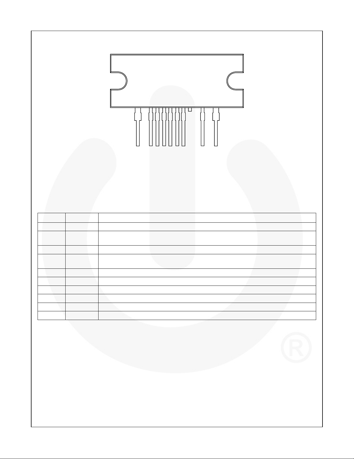
Pin Configuration
1 2 3 4 5 6 7 8 9 10
CSSGPG
LVcc
HVcc
V
DL
R
T
V
FB
Figure 4. Package Diagram
FSFA2100 — Fairchild Power Switch (FPS™) for Half-Bridge PWM Converter
V
CTR
Pin Definitions
Pin # Name Description
1 VDL This is the drain of the high-side MOSFET, typically connected to the input DC link voltage.
2 VFB
3 RT This pin programs the switching frequency using a resistor.
4 CS
5 SG This pin is the control ground.
6 PG This pin is the power ground. This pin is connected to the source of the low-side MOSFET.
7 LVCC This pin is the supply voltage of the control IC.
8 NC No connection.
9 HVCC This is the supply voltage of the high-side gate-drive circuit IC.
10 V
CTR
This pin is connected to the inverting input of the PWM comparator internally and to the
opto-coupler externally. The duty cycle is determined by the voltage on this pin.
This pin senses the current flowing through the low-side MOSFET. Typically, negative
voltage is applied on this pin.
This is the drain of the low-side MOSFET. Typically, a transformer is connected to this pin.
© 2008 Fairchild Semiconductor Corporation www.fairchildsemi.com
FSFA2100 • Rev. 1.0.0 4
Page 5
FSFA2100 — Fairchild Power Switch (FPS™) for Half-Bridge PWM Converter
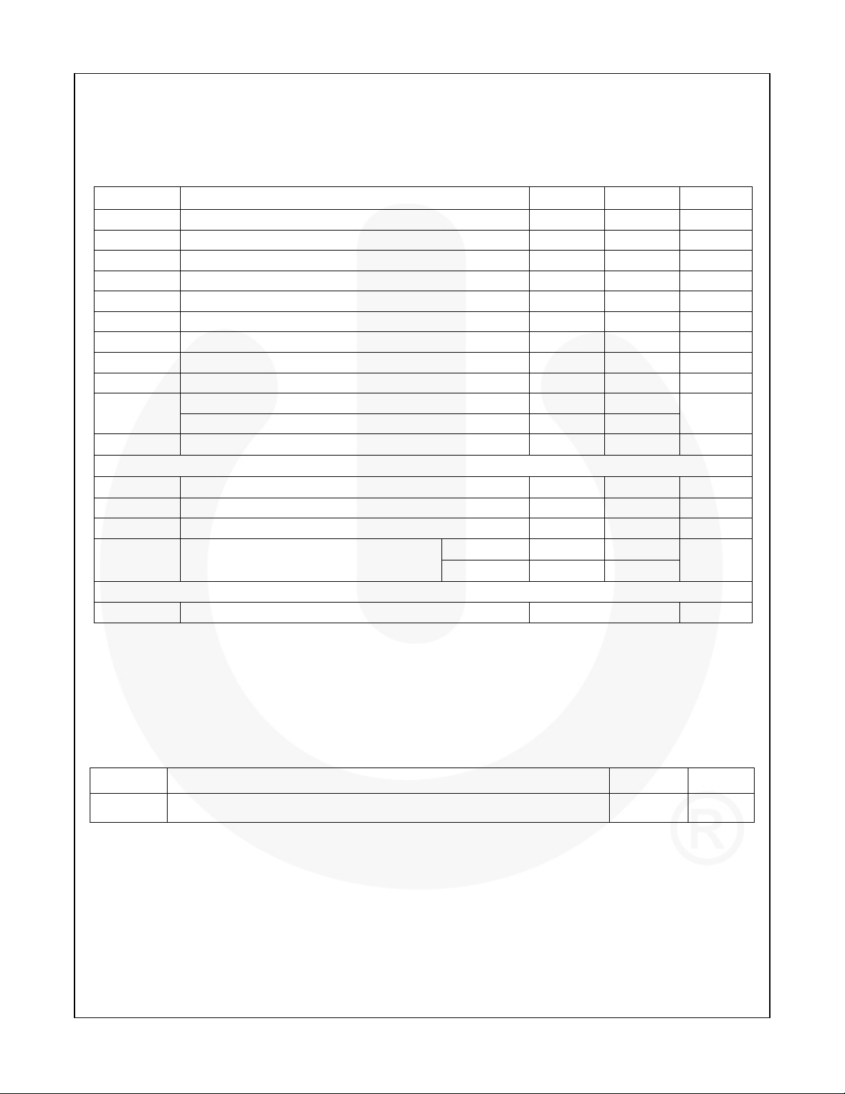
Absolute Maximum Ratings
Stresses exceeding the absolute maximum ratings may damage the device. The device may not function or be
operable above the recommended operating conditions and stressing the parts to these levels is not recommended. In
addition, extended exposure to stresses above the recommended operating conditions may affect device reliability.
The absolute maximum ratings are stress ratings only. T
Symbol Parameter Min. Max. Unit
VDS Maximum Drain-to-Source Voltage (VDL-V
LVCC Low-Side Supply Voltage -0.3 25.0 V
HVCC to V
HVCC High-Side Floating Supply Voltage -0.3 625.0 V
VFB Feedback Pin Input Voltage -0.3 LVCC V
VCS Current Sense (CS) Pin Input Voltage -5.0 1.0 V
VRT R
dV
CTR
PD Total Power Dissipation
TJ
T
MOSFET Section
V
DGR
VGS Gate Source (GND) Voltage ±30 V
IDM Drain Current Pulsed 33 A
Package Section
Torque Recommended Screw Torque 5~7 kgf·cm
Notes:
3. Per MOSFET when both MOSFETs are conducting.
4. The maximum value of the recommended operating junction temperature is limited by thermal shutdown.
High-Side VCC Pin to Low-Side Drain Voltage -0.3 25.0 V
CTR
Pin Input Voltage -0.3 5.0 V
T
/dt Allowable Low-Side MOSFET Drain Voltage Slew Rate 50 V/ns
(3)
12.0 W
Maximum Junction Temperature
(4)
Recommended Operating Junction Temperature
Storage Temperature Range -55 +150
STG
Drain Gate Voltage (RGS=1MΩ)
ID Continuous Drain Current
=25°C unless otherwise specified.
A
and V
CTR
+150
(4)
) 600 V
CTR-PG
-40 +130
°C
°C
600 V
TC=25°C
T
=100°C
C
11
7
A
Thermal Impedance
TA=25°C unless otherwise specified.
Symbol Parameter Value Unit
θJC Junction-to-Case Center Thermal Impedance (Both MOSFETs Conducting) 10.44 ºC/W
© 2008 Fairchild Semiconductor Corporation www.fairchildsemi.com
FSFA2100 • Rev. 1.0.0 5
Page 6

Electrical Characteristics
TA=25°C and LVCC=17V unless otherwise specified.
Symbol Parameter Test Conditions Min. Typ. Max. Unit
MOSFET Section
FSFA2100 — Fairchild Power Switch (FPS™) for Half-Bridge PWM Converter
BV
Drain-to-Source Breakdown Voltage
DSS
ID=200μA, TA=125°C
R
On-State Resistance VGS=10V, ID=5.5A 0.32 0.38
DS(ON)
ID=200μA, TA=25°C
t
Body Diode Reverse Recovery Time
rr
(5)
VGS=0V, I
dI
/dt=100A/μs
Diode
Diode
=11.0A,
600
V
650
Ω
120 ns
Supply Section
ILK Offset Supply Leakage Current HVCC=V
=600V 50 μA
CTR
IQHVCC Quiescent HVCC Supply Current (HVCCUV+) - 0.1V 50 120 μA
IQLVCC Quiescent LVCC Supply Current (LVCCUV+) - 0.1V 100 200 μA
f
=100KHz, VFB > 3V
IOHVCC
IOLVCC
Operating HV
(RMS Value)
Operating LV
(RMS Value)
Supply Current
CC
Supply Current
CC
OSC
=17V
HV
CC
No switching, V
=17V
HV
CC
f
=100KHz, VFB > 3V 7 11 mA
OSC
No switching, V
< 1V
FB
< 1V 2 4 mA
FB
6 9 mA
100 200 μA
UVLO Section
LVCCUV+ LVCC Supply Under-Voltage Positive Going Threshold (LVCC Start) 13.0 14.5 16.0 V
LVCCUV- LVCC Supply Under-Voltage Negative Going Threshold (LVCC Stop) 10.2 11.3 12.4 V
LVCCUVH LVCC Supply Under-Voltage Hysteresis 3.2 V
HVCCUV+ HVCC Supply Under-Voltage Positive Going Threshold (HVCC Start) 8.2 9.2 10.2 V
HV
HVCCUV-
Supply Under-Voltage Negative Going Threshold (HVCC Stop)
CC
7.8 8.7 9.6 V
HVCCUVH HVCC Supply Under-Voltage Hysteresis 0.5 V
Oscillator and Feedback Section
VRT V-I Converter Threshold Voltage 1.5 2.0 2.5 V
f
Output Oscillation Frequency
OSC
D
Maximum Duty Cycle VFB=4V 45 50 55 %
MAX
D
Minimum Duty Cycle VFB=0V 0 %
MIN
MAX
V
Maximum Feedback Voltage for D
FB
MAX
RT=27KΩ
D
MAX
≥ 48% 2.7 3.0 3.3 V
94 100 106 KHz
IFB Feedback Source Current VFB=0V 370 470 570 μA
VBH Burst Mode High-Threshold Voltage 1.34 1.50 1.66 V
VBL Burst Mode Low-Threshold Voltage 1.16 1.30 1.44 V
V
Burst Mode Hysteresis Voltage 0.1 0.2 0.3 V
BHY
tSS Internal Soft-Start Time f
=100kHz 10 15 20 ms
OSC
Continued on the following page…
© 2008 Fairchild Semiconductor Corporation www.fairchildsemi.com
FSFA2100 • Rev. 1.0.0 6
Page 7

FSFA2100 — Fairchild Power Switch (FPS™) for Half-Bridge PWM Converter
Electrical Characteristics (Continued)
TA=25°C and LVCC=17V unless otherwise specified.
Symbol Parameter Test Conditions Min. Typ. Max. Unit
Protection Section
I
OLP Delay Current VFB=5V 3.8 5.0 6.2 μA
OLP
V
OLP Protection Voltage VFB > 6V 6.3 7.0 7.7 V
OLP
V
LVCC Over-Voltage Protection LVCC > 21V 21 23 25 V
OVP
V
AOCP Threshold Voltage
AOCP
t
AOCP Blanking Time
BAO
tDA Delay Time (Low-Side) from V
V
Pulse-by-Pulse Current Limit Threshold Voltage
LIM
(5)
to Switch Off
AOCP
tBL Pulse-by-Pulse Current Limit Blanking Time
tDL Delay Time (Low-Side) from V
TSD Thermal Shutdown Temperature
to Switch Off
LIM
(5)
110 130 150
(5)
(5)
ΔV/Δt=-1V/µs
VCS < V
AOCP
;
ΔV/Δt=-1V/µs
ΔV/Δt=-1V/µs
ΔV/Δt=-0.1V/µs
VCS < V
LIM
;
ΔV/Δt=-0.1V/µs
ΔV/Δt=-0.1V/µs
ISU Protection Latch Sustain LVCC Supply Current LVCC=7.5V 100 150 μA
V
Protection Latch Reset LVCC Supply Voltage 5 V
PRSET
Dead-Time Control Section
DT Dead Time
(6)
200 ns
Notes:
5. This parameter, although guaranteed, is not tested in production.
6. These parameters, although guaranteed, are tested only in EDS (wafer test) process.
-1.0 -0.9 -0.8 V
50 ns
250 400 ns
-0.64 -0.58 -0.52 V
150 ns
450 ns
°C
© 2008 Fairchild Semiconductor Corporation www.fairchildsemi.com
FSFA2100 • Rev. 1.0.0 7
Page 8
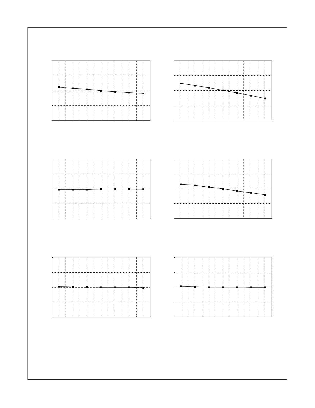
Typical Performance Characteristics
These characteristic graphs are normalized at TA=25ºC.
FSFA2100 — Fairchild Power Switch (FPS™) for Half-Bridge PWM Converter
1.1
1.05
℃
1
Normalized at 25
0.95
0.9
-40 -20 0 25 50 75 100
Temp (℃)
1.1
1.05
℃
1
Normali zed at 25
0.95
0.9
-40-200 255075100
Temp (℃)
Figure 5. Maximum Duty Cycle vs. Temperature Figure 6. Switching Frequency vs. Temperature
1.1
1.05
℃
1
Normalized at 25
0.95
1.1
1.05
℃
1
Normali zed at 25
0.95
0.9
-40 -20 0 25 50 75 100
Temp (℃)
0.9
-40-200 255075100
Temp (℃)
Figure 7. High-Side VCC (HVCC) Start vs. Temperature Figure 8. High-Side VCC (HVCC) Stop vs. Temperature
1.1
1.05
℃
1
Normalized at 25
0.95
0.9
-40 -20 0 25 50 75 100
Temp (℃)
1.1
1.05
℃
1
Normali zed at 25
0.95
0.9
-40-20 0 255075100
Temp (℃)
Figure 9. Low-Side V
(LVCC) Start vs. Temperature Figure 10. Low-Side VCC (LVCC) Stop vs. Temperature
CC
© 2008 Fairchild Semiconductor Corporation www.fairchildsemi.com
FSFA2100 • Rev. 1.0.0 8
Page 9
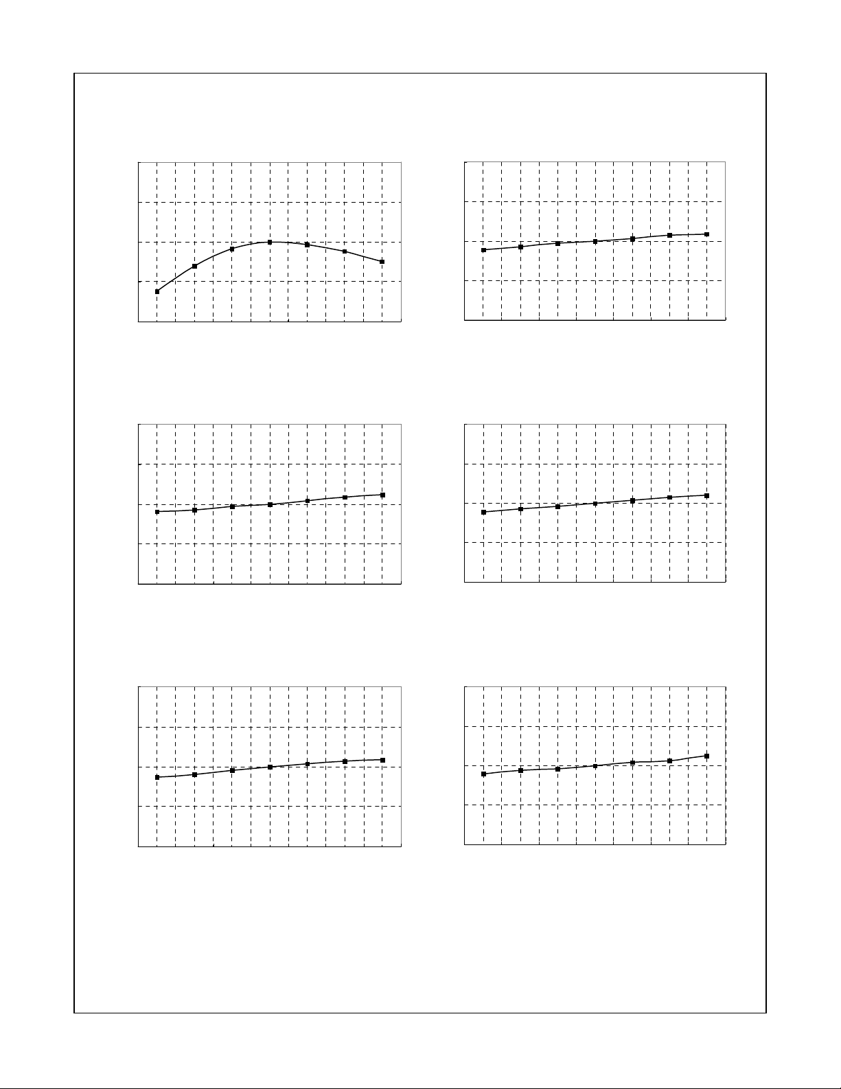
Typical Performance Characteristics (Continued)
These characteristic graphs are normalized at TA=25ºC.
FSFA2100 — Fairchild Power Switch (FPS™) for Half-Bridge PWM Converter
1.1
1.05
℃
1
Normalized at 25
0.95
0.9
-40 -20 0 25 50 75 100
Temp (℃)
1.1
1.05
℃
1
Normaliz ed at 25
0.95
0.9
-40-20 0 255075100
Temp (℃)
Figure 11. OLP Delay Current vs. Temperature Figure 12. OLP Voltage vs. Temperature
1.1
1.05
℃
1
Normalized at 25
0.95
1.1
1.05
℃
1
Normalized at 25
0.95
0.9
-40 -20 0 25 50 75 100
Temp (℃)
0.9
-40-200 255075100
Temp (℃)
Figure 13. LVCC OVP Voltage vs. Temperature Figure 14. RT Voltage vs. Temperature
1.1
1.05
℃
1
Normalized at 25
0.95
0.9
-40 -20 0 25 50 75 100
Temp (℃)
1.1
1.05
℃
1
Normalized at 25
0.95
0.9
-40-200 255075100
Temp (℃)
Figure 15. VBH Voltage vs. Temperature Figure 16. V
Voltage vs. Temperature
LIM
© 2008 Fairchild Semiconductor Corporation www.fairchildsemi.com
FSFA2100 • Rev. 1.0.0 9
Page 10
Functional Description
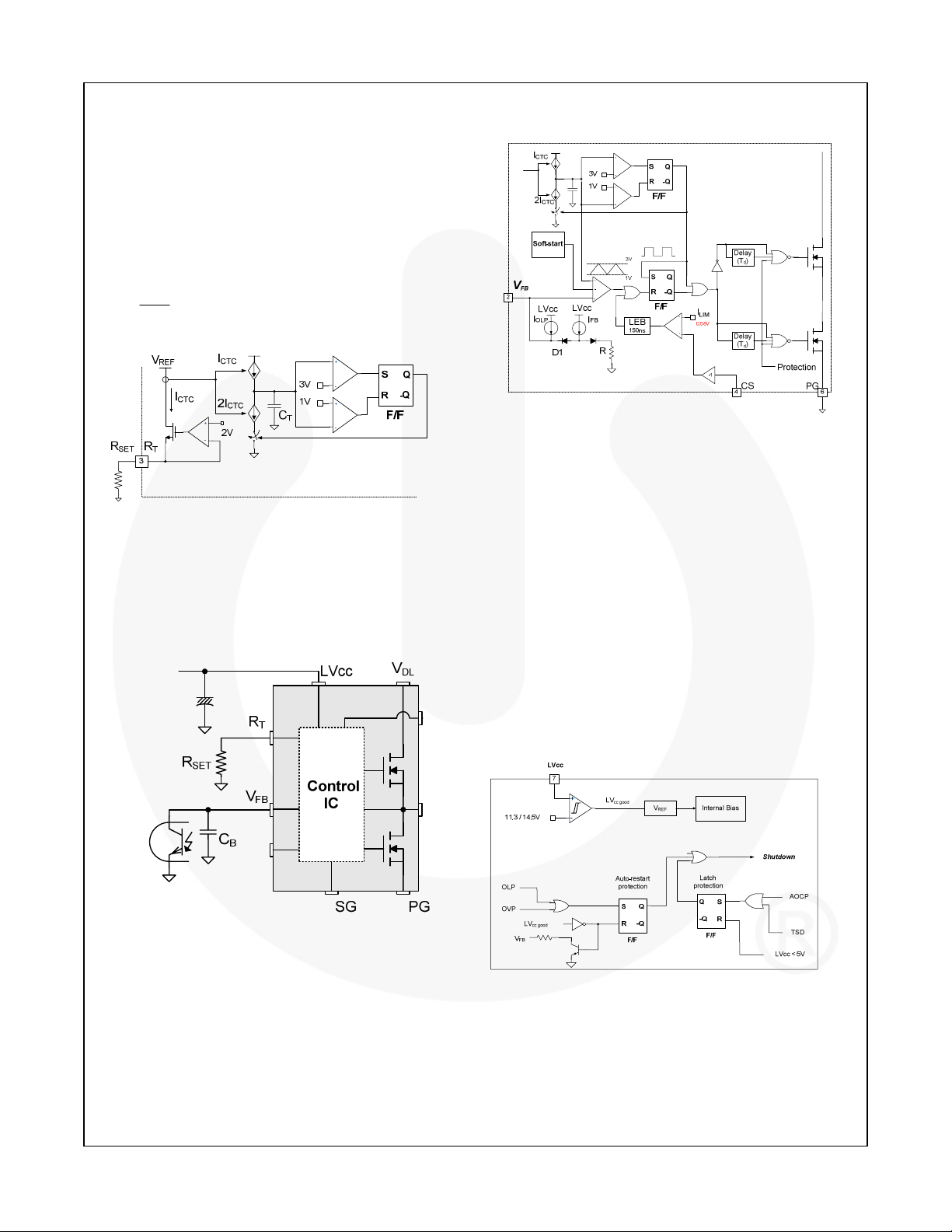
1. Internal Oscillator: FSFA2100 employs a current-
controlled oscillator as shown in Figure 17. Internally, the
voltage of the R
pin is regulated at 2V and the
T
charging/discharging current for the oscillator capacitor
C
is determined by the current flowing out of the RT pin
T
(I
). When the RT pin is pulled down to the ground with
CTC
a resistor R
, the switching frequency is fixed as:
SET
k
27
Ω
f
S
×
=
R
SET
kHz
)(100
(1)
Figure 17. Current Controlled Oscillator
2. PWM Control: Figure 18 shows the typical control
circuit configuration. The opto-coupler transistor should
be connected to the VFB pin in parallel with the feedback
capacitor to control the duty cycle.
Figure 19. Internal PWM Block Diagram
3. Protection Circuits: The FSFA2100 has Overload
Protection (OLP), Abnormal Over-Current Protection
(AOCP), Over-Voltage Protection (OVP), and Thermal
Shutdown (TSD) self-protective functions. The OLP and
OVP are auto-restart mode protections, while the AOCP and
TSD are latch-mode protections, as shown in Figure 20.
Auto-restart mode protection: Once the fault condition is
detected, the switching is terminated and the MOSFETs
remain off. When LV
falls down to LVCC stop voltage of
CC
around 11V, the protection is reset. The FPS resumes
normal operation when LV
reaches the start voltage of
CC
about 14V.
Latch-mode protection: Once this protection is triggered,
the switching is terminated and the MOSFETs remain
off. The latch is reset only when LV
is discharged
CC
below 5V.
FSFA2100 — Fairchild Power Switch (FPS™) for Half-Bridge PWM Converter
Figure 18. PWM Control Configuration
Figure 19 shows the internal block diagram for PWM
operation. Duty cycle is controlled by comparing the
feedback voltage to the triangular signal with a range
from 1V to 3V.
Figure 20. Protection blocks
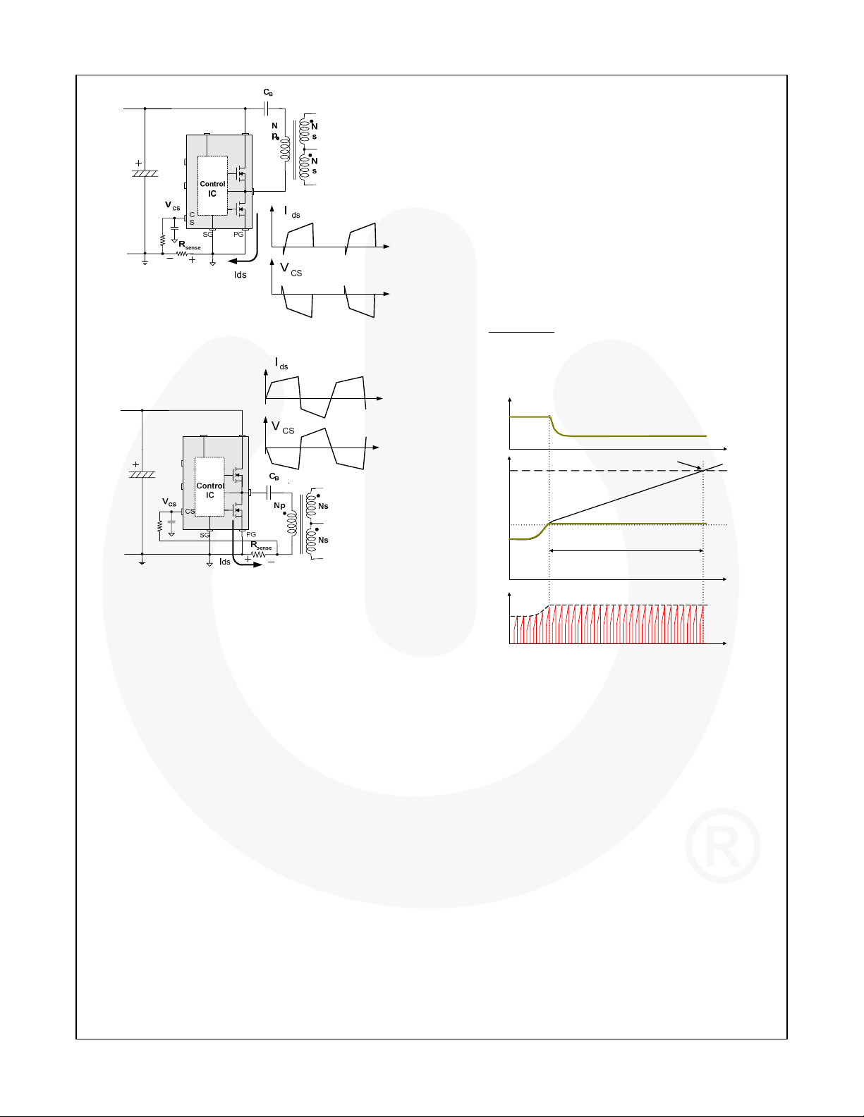
Low-side MOSFET current should be sensed for Pulseby-pulse current limit and AOCP. The FSFA2100 senses
drain current as a negative voltage, as shown in Figure
21 and Figure 22. Half-wave sensing allows low-power
dissipation in the sensing resistor, while full-wave
sensing has less noise in the sensing signal.
© 2008 Fairchild Semiconductor Corporation www.fairchildsemi.com
FSFA2100 • Rev. 1.0.0 10
Page 11
FSFA2100 — Fairchild Power Switch (FPS™) for Half-Bridge PWM Converter
through the MOSFET is limited; and, therefore, the
maximum input power is restricted with a given input
voltage. If the output consumes more than this maximum
Figure 21. Half-Wave Sensing
power, the output voltage (V
nominal voltage. This reduces the current through the
opto-coupler diode, which also reduces the opto-coupler
transistor current, increasing the feedback voltage (V
If V
exceeds 3V, D1, which is illustrated in Figure 19, is
FB
blocked and the OLP current source starts to charge C
slowly, as shown in Figure 23. In this condition, V
continues increasing until it reaches 7V, then the
switching operation is terminated, as shown in Figure 23.
The delay time for shutdown is the time required to
charge C
from 3V to 7V with 5µA, as given by:
B
t
delay
=
CVV
)37( ×
-
B
A
μ
5
A 30 ~ 50ms delay time is typical for most applications.
V
O
) decreases below the
O
FB
(2)
).
B
FB
Figure 22. Full-Wave Sensing
3.1 Pulse-by-Pulse Current Limit: In normal operation,
the duty cycle of the low-side MOSFET is determined by
comparing the internal triangular signal with the
feedback voltage. However, the low-side MOSFET is
forced to turn off when the current sense pin voltage
reaches -0.58V. This operation limits the drain current
below a pre-determined level to avoid the destruction of
the MOSFETs.
3.2 Abnormal Over-Current Protection (AOCP): If one
of the secondary rectifier diodes is short-circuited, large
current with extremely high di/dt can flow through the
MOSFET before OCP or OLP is triggered. AOCP is
triggered with a very short shutdown delay time when the
sensed voltage drops below -0.9V. This protection is
latch mode and reset only when LV
is pulled below 5V.
CC
3.3 Overload Protection (OLP): Overload is defined as
the load current exceeding its nominal level due to an
unexpected abnormal event. In this situation, a
protection circuit should trigger to protect the power
supply. However, even when the power supply is in the
normal condition, the OLP circuit can be triggered during
the load transition. To avoid this undesired operation, the
OLP circuit is designed to trigger only after a specified
time to determine whether it is a transient situation or a
true overload situation. Because of the pulse-by-pulse
current limit capability, the maximum peak current
7V
3V
I
ds
t
Overload protection
V
FB
Vc
t
delay
1 t
t
2
I
LIM
Figure 23. Overload Protection
3.4 Over-Voltage Protection (OVP): When the LV
CC
reaches 23V, OVP is triggered. This protection is
enabled when using an auxiliary winding of the
transformer to supply LV
to FPS.
CC
3.5 Thermal Shutdown (TSD): The MOSFETs and the
control IC are built in one package. This allows the
control IC to detect the abnormal over-temperature of the
MOSFET. If the temperature exceeds approximately
°C, the thermal shutdown triggers.
130
4. Soft-Start: At startup, the duty cycle starts increasing
slowly to establish the correct working conditions for
transformers, inductors, and capacitors. The voltage on
the output capacitors is progressively increased to
smoothly establish the required output voltage. Soft-start
time is internally implemented for 15ms (when the
operating frequency is set to 100kHz.) In addition, to
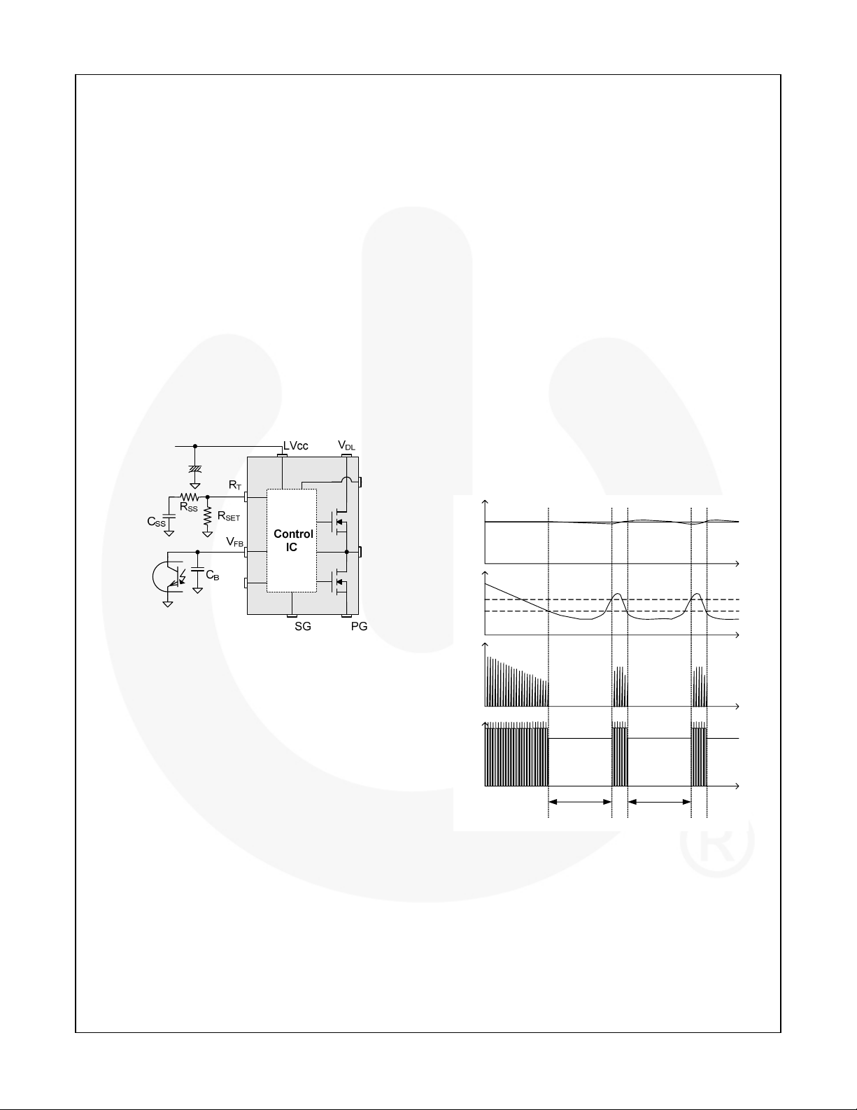
help the soft-start operation, a capacitor and a resistor
would be connected on the R
pin externally, as shown
T
in Figure 24. Before the power supply is powered on, the
capacitor C
becomes charged progressively by the current
C
SS
remains fully discharged. After power-on,
SS
© 2008 Fairchild Semiconductor Corporation www.fairchildsemi.com
FSFA2100 • Rev. 1.0.0 11
Page 12
through the RT pin, which determines the operating
frequency. The current through the R
pin is inversely
T
proportional to the total impedance of the connected
resistors. The total impedance at startup is lower than
that of the normal operation because R
in parallel, which means the operating frequency
R
SET
is added on
SS
decreases continuously from higher to nominal.
Eventually C
the operating frequency is determined by R
During the charging time of C
is fully charged to the RT pin voltage and
SS
, the operating frequency
SS
SET
only.
is higher than during normal operation. In asymmetric
half-bridge converters, a switching period contains
powering and commutation periods. The energy cannot
be transferred to the output side during commutation
period. Since the DC link voltage applied to the V
DL
pin
and the leakage inductance of the main transformer are
fixed, the powering period over the switching period is
shorter in high switching frequencies. As C
is charged,
SS
the switching frequency decreases and the powering
period over the switching period increases as well. It is
helpful to start SMPS softly with the internal soft-start
time together.
applied voltage make an excessive primary current.
When the high-side MOSFET turns off, the primary
current flows back to the DC link capacitor through the
body diode of the low-side MOSFET. It keeps the same
status even after turning on and off the low-side
MOSFET. When the high-side MOSFET turns on again,
a huge current can flow from the DC link capacitor
through the channel of the high-side MOSFET and body
diode of the low-side one due to the reverse recovery. It
may induce unexpected noise into CS pin.
To avoid this issue, the voltage across the DC blocking
capacitor must be low enough. In general, two resistors
with several MHz can be added on the drain-to-source
terminals of each MOSFET to divide the DC link voltage.
6. Burst Operation: To minimize power dissipation in
standby mode, the FSFA2100 enters burst-mode
operation. As the load decreases, the feedback voltage
decreases. As shown in Figure 25, the device
automatically enters burst mode when the feedback
voltage drops below V
(1.3V). At this point, switching
BL
stops and the output voltages start to drop at a rate
dependent on standby current load. This causes the
feedback voltage to rise. Once it passes V
(1.5V),
BH
switching resumes. The feedback voltage then falls and
the process repeats. Burst-mode operation alternately
enables and disables switching of the MOSFETs,
thereby reducing switching loss in standby mode.
FSFA2100 — Fairchild Power Switch (FPS™) for Half-Bridge PWM Converter
Figure 24. External Soft-Start Circuit
5. Startup: Due to the imbalance of the turn-off
resistance between the high- and low-side MOSFETs,
the voltage across the DC blocking capacitor cannot be
predicted at startup. Additionally, the high-side MOSFET
starts with a large duty cycle since the duty cycle of the
low-side MOSFET increases step-by-step during softstart time. Therefore, in the case where high voltage is
already charged in the DC blocking capacitor due to the
higher turn-off resistance of the high-side MOSFET
before startup, a large primary current could flow through
the high-side MOSFET during turn-on time after startup.
For the high-side MOSFET, a long duty cycle and high
V
O
set
Vo
V
FB
1.5V
1.3V
I
ds
V
ds
Switching
stop
t
1
Figure 25. Burst-Mode Operation
t2t
3
Switching
stop
t
t
4
© 2008 Fairchild Semiconductor Corporation www.fairchildsemi.com
FSFA2100 • Rev. 1.0.0 12
Page 13
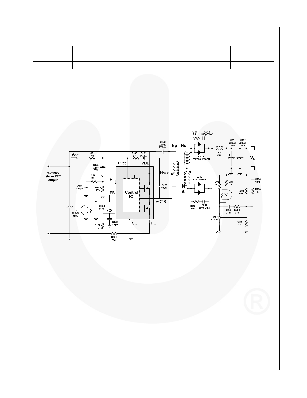
Typical Application Circuit (Asymmetric PWM Half-Bridge Converter)
FSFA2100 — Fairchild Power Switch (FPS™) for Half-Bridge PWM Converter
Application FPS™ Device Input Voltage Range Rated Output Power
LCD TV FSFA2100 400V 200W 25V-8A
Output Voltage
(Rated Current)
Features
High Efficiency ( >93% at 400V
input)
IN
Reduced EMI Noise through Zero-Voltage-Switching (ZVS)
Enhanced System Reliability with Various Protection Functions
Internal Soft-Start (15ms)
Figure 26. Typical Application Circuit
© 2008 Fairchild Semiconductor Corporation www.fairchildsemi.com
FSFA2100 • Rev. 1.0.0 13
Page 14
Typical Application Circuit (Continued)
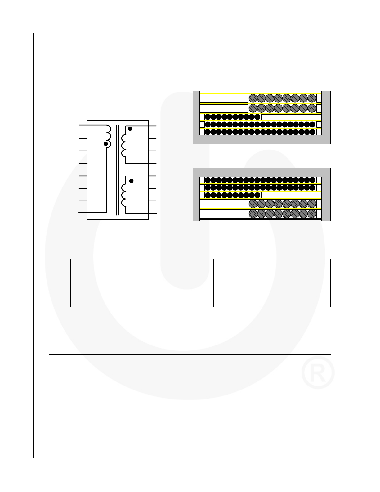
Core: EER3542 (Ae=107 mm
2
)
Bobbin: EER3542 (Horizontal)
EER3542
1
N
p
89
16
N
s1
1
3
1
2
N
s2
FSFA2100 — Fairchild Power Switch (FPS™) for Half-Bridge PWM Converter
Figure 27. Core and Winding
Pin(S → F) Wire Turns Winding Method
Np 8 → 1 0.12φ×30 (Litz wire) 50 Solenoid winding
Ns1 16 → 13 0.1φ×100 (Litz wire) 8 Solenoid winding
Ns2 12 → 9 0.1φ×100 (Litz wire) 8 Solenoid winding
Pin Specification Remark
Inductance 1-8
Leakage 1-8
μH ± 5%
630
μH ± 10%
45
Short one of the secondary windings
100kHz, 1V
© 2008 Fairchild Semiconductor Corporation www.fairchildsemi.com
FSFA2100 • Rev. 1.0.0 14
Page 15
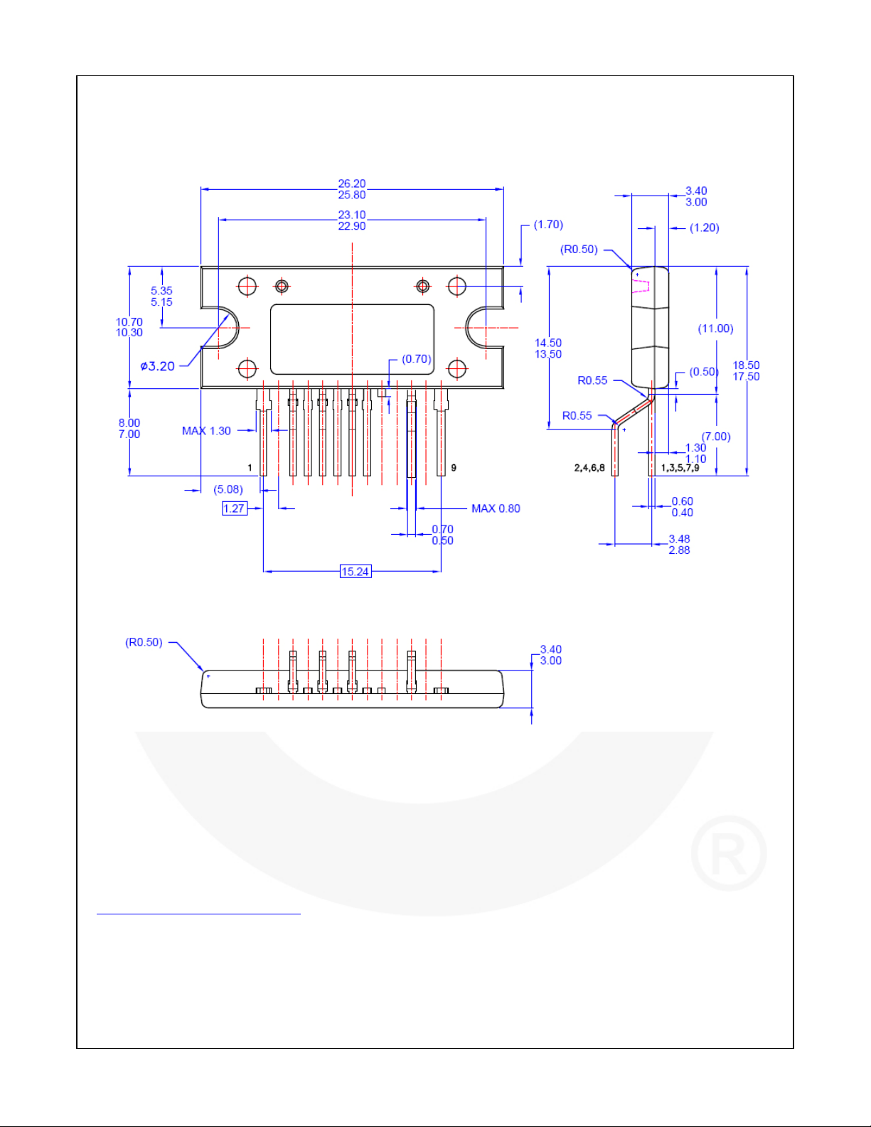
Physical Dimensions
FSFA2100 — Fairchild Power Switch (FPS™) for Half-Bridge PWM Converter
SIPMODAA09RevA
Figure 28. 9-SIP Package
Package drawings are provided as a service to customers consideri ng Fai rchild components. Drawings may change in any manner
without notice. Pl ease note the revision and/or date on the drawing and c ontact a Fairchild Semiconductor representat i ve to verify or
obtain the most recent revis i on. Package specifications do not expand the terms of Fairchild’s worldwide terms and condi tions,
specifically t he warranty therein, which covers Fai rchild products.
Always visi t Fai rchild Semiconductor’s online packaging area for the most recent package drawings:
http://www.fairchildsemi.com/packaging/
© 2008 Fairchild Semiconductor Corporation www.fairchildsemi.com
FSFA2100 • Rev. 1.0.0 15
.
Page 16
FSFA2100 — Fairchild Power Switch (FPS™) for Half-Bridge PWM Converter
© 2008 Fairchild Semiconductor Corporation www.fairchildsemi.com
FSFA2100 • Rev. 1.0.0 16
 Loading...