

Page 1
FSBF5CH60B
Smart Power Module
FSBF5CH60B Smart Power Module
June 2007
TM
Motion-SPM
Features
• UL Certified No.E209204(SPM27-JA package)
• 600V-5A 3-phase IGBT inverter bridge including control ICs
for gate driving and protection
• Easy PCB layout due to built in bootstrap diode
• Divided negative dc-link terminals for inverter current sensing
applications
• Single-grounded power supply due to built-in HVIC
• Isolation rating of 2500Vrms/min.
Applications
• AC 100V ~ 253V three-phase inverter drive for small power
ac motor drives
• Home appliances applications like air conditioner and washing machine
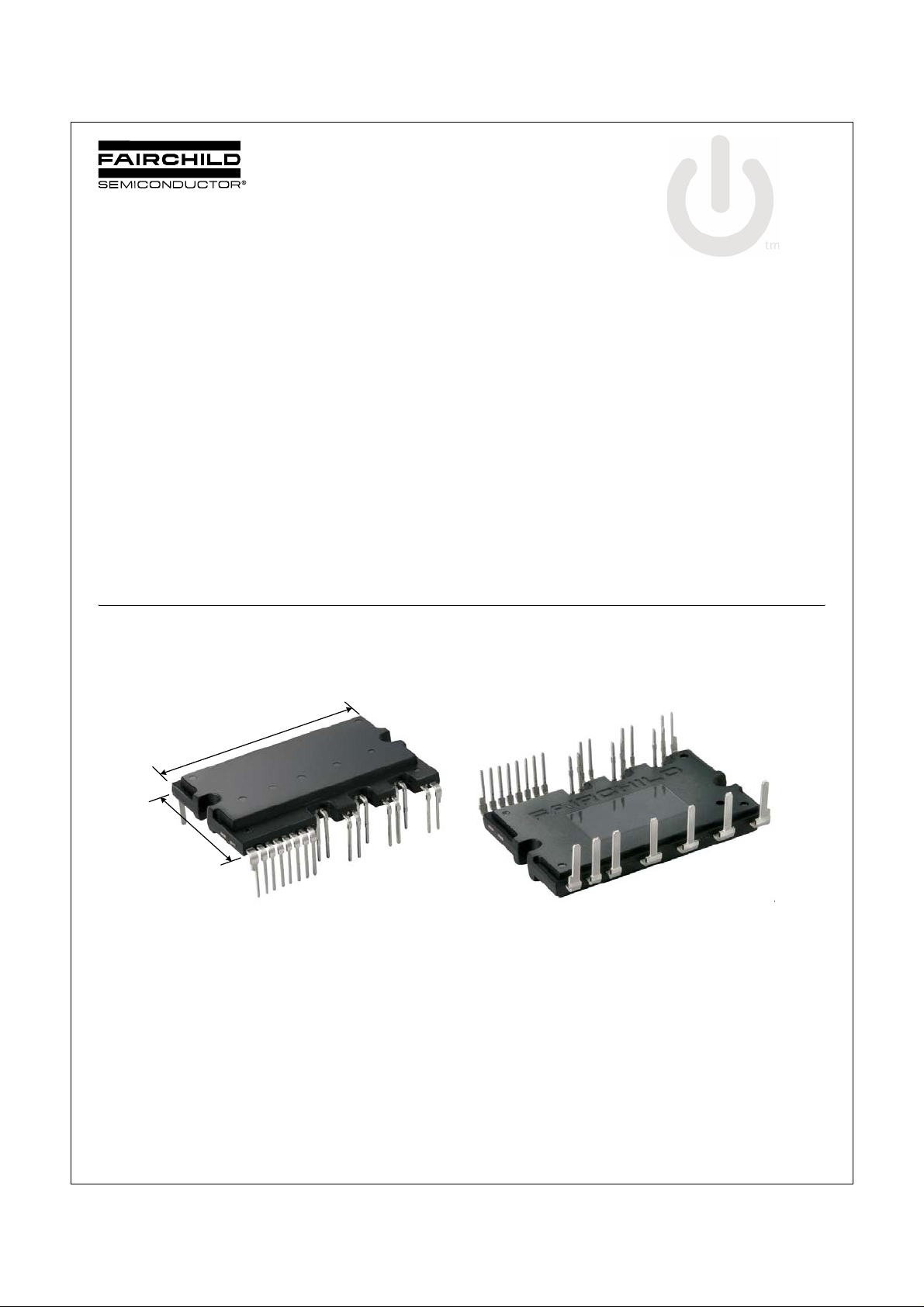
Top View Bottom View
44mm
General Description
It is an advanced motion-smart power module (Motion-SPMTM)
that Fairchild has newly developed and designed to provide
very compact and high performance ac motor drives mainly targeting low-power inverter-driven application like air conditioner
and washing machine. It combines optimized circuit protection
and drive matched to low-loss IGBTs. System reliability is further enhanced by the integrated under-voltage lock-out and
short-circuit protection. The high speed built-in HVIC provides
opto-coupler-less single-supply IGBT gate driving capability that
further reduce the overall size of the inverter system design.
Each phase current of inverter can be monitored separately due
to the divided negative dc terminals.
26.8mm
Figure 1.
©2007 Fairchild Semiconductor Corporation 1 www.fairchildsemi.com
FSBF5CH60B Rev. C
Page 2
Integrated Power Functions
• 600V-5A IGBT inverter for three-phase DC/AC power conversion (Please refer to Figure 3)
Integrated Drive, Protection and System Control Functions
• For inverter high-side IGBTs: Gate drive circuit, High voltage isolated high-speed level shifting
Control circuit under-voltage (UV) protection
Note) Available bootstrap circuit example is given in Figures 10 and 11.
• For inverter low-side IGBTs: Gate drive circuit, Short circuit protection (SC)
Control supply circuit under-voltage (UV) protection
• Fault signaling: Corresponding to UV (Low-side supply) and SC faults
• Input interface: 3.3/5V CMOS/LSTTL compatible, Schmitt trigger input
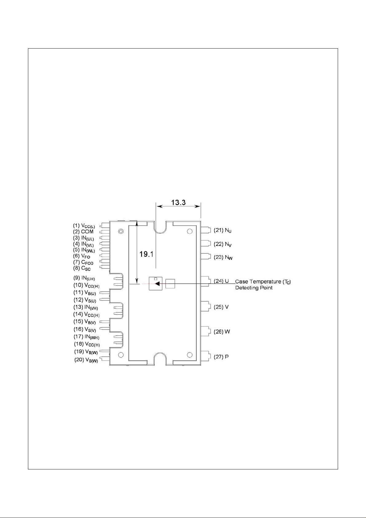
Pin Configuration
Top View
FSBF5CH60B Smart Power Module
FSBF5CH60B Rev. C
Figure 2.
2 www.fairchildsemi.com
Page 3
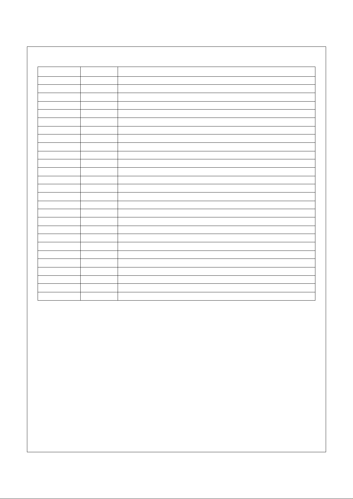
Pin Descriptions
Pin Number Pin Name Pin Description
1V
CC(L)
2 COM Common Supply Ground
3IN
4IN
5IN
6V
7C
8C
9IN
10 V
11 V
12 V
13 IN
14 V
15 V
16 V
17 IN
18 V
19 V
20 V
21 N
22 N
23 N
(UL)
(VL)
(WL)
FO
FOD
SC
(UH)
CC(H)
B(U)
S(U)
(VH)
CC(H)
B(V)
S(V)
(WH)
CC(H)
B(W)
S(W)
U
V
W
24 U Output for U Phase
25 V Output for V Phase
26 W Output for W Phase
27 P Positive DC–Link Input
Low-side Common Bias Voltage for IC and IGBTs Driving
Signal Input for Low-side U Phase
Signal Input for Low-side V Phase
Signal Input for Low-side W Phase
Fault Output
Capacitor for Fault Output Duration Time Selection
Capacitor (Low-pass Filter) for Short-Current Detection Input
Signal Input for High-side U Phase
High-side Common Bias Voltage for IC and IGBTs Driving
High-side Bias Voltage for U Phase IGBT Driving
High-side Bias Voltage Ground for U Phase IGBT Driving
Signal Input for High-side V Phase
High-side Common Bias Voltage for IC and IGBTs Driving
High-side Bias Voltage for V Phase IGBT Driving
High-side Bias Voltage Ground for V Phase IGBT Driving
Signal Input for High-side W Phase
High-side Common Bias Voltage for IC and IGBTs Driving
High-side Bias Voltage for W Phase IGBT Driving
High-side Bias Voltage Ground for W Phase IGBT Driving
Negative DC–Link Input for U Phase
Negative DC–Link Input for V Phase
Negative DC–Link Input for W Phase
FSBF5CH60B Smart Power Module
FSBF5CH60B Rev. C
3 www.fairchildsemi.com
Page 4
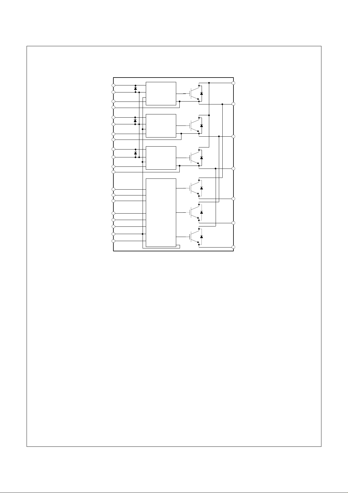
Internal Equivalent Circuit and Input/Output Pins
FSBF5CH60B Smart Power Module
(19) V
(18) V
(17) IN
(20) V
(15) V
(14) V
(13) IN
(16) V
(11) V
(10) V
(9) IN
(12) V
(8) C
(7) C
(6) V
(5) IN
(4) IN
(3) IN
(2) COM
(1) V
(UH)
B(W)
CC(H)
S(W)
B(V)
CC(H)
(VH)
S(V)
B(U)
CC(H)
S(U)
SC
FOD
FO
CC(L)
(WH)
(WL)
(VL)
(UL)
VB
VCC
COM
IN
VB
VCC
COM
IN
VB
VCC
COM
IN
C(SC)
C(FOD)
VFO
IN(WL)
IN(VL)
IN(UL)
COM
VCC
OUT
VS
OUT
VS
OUT
VS
OUT(WL)
OUT(VL)
OUT(UL)
V
P (27)
W (26)
V (25)
U (24)
N
(23)
W
(22)
N
V
SL
NU (21)
Note:
1. Inverter low-side is composed of three IGBTs, freewheeling diodes for each IGBT and one control IC. It has gate drive and protection functions.
2. Inverter power side is composed of four inverter dc-link input terminals and three inverter output terminals.
3. Inverter high-side is composed of three IGBTs, freewheeling diodes and three drive ICs for each IGBT.
Figure 3.
FSBF5CH60B Rev. C
4 www.fairchildsemi.com
Page 5
FSBF5CH60B Smart Power Module
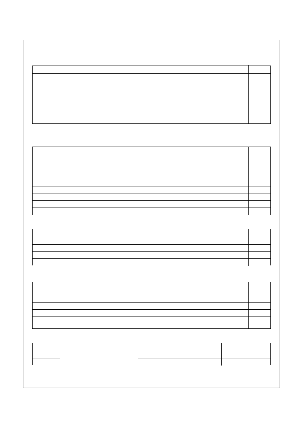
Absolute Maximum Ratings (T
= 25°C, Unless Otherwise Specified)
J
Inverter Part
Symbol Parameter Conditions Rating Units
V
PN
V
PN(Surge)
V
CES
± I
± I
CP
P
C
T
Note:
1. The maximum junction temperature rating of the power chips integrated within the SPM is 150°C(@T
Supply Voltage Applied between P- NU, NV, N
Supply Voltage (Surge) Applied between P- NU, NV, N
W
W
Collector-emitter Voltage 600 V
Each IGBT Collector Current TC = 25°C 5 A
C
Each IGBT Collector Current (Peak) TC = 25°C, Under 1ms Pulse Width 10 A
Collector Dissipation TC = 25°C per One Chip 19 W
Operating Junction Temperature (Note 1) -40 ~ 150 °C
J
≤ 125°C).
C
450 V
500 V
Control Part
Symbol Parameter Conditions Rating Units
V
CC
V
BS
V
IN
V
FO
I
FO
V
SC
T
J(Driver IC)
Control Supply Voltage Applied between V
High-side Control Bias
Voltage
Applied between V
V
- V
B(W)
S(W)
Input Signal Voltage Applied between IN
IN
, IN
(VL)
, IN
(UL)
(WL)
CC(H)
B(U)
(UH)
- COM
- V
, V
- COM 20 V
CC(L)
, V
- V
S(U)
, IN
(VH)
B(V)
, IN
S(V)
(WH)
,
,
-0.3~17 V
20 V
Fault Output Supply Voltage Applied between VFO - COM -0.3~VCC+0.3 V
Fault Output Current Sink Current at VFO Pin 5 mA
Current Sensing Input Voltage Applied between CSC - COM -0 .3~VCC+0.3 V
Operating Junction Temperature -40 ~ 150 °C
Bootstrap Diode Part
Symbol Parameter Conditions Rating Units
V
RRM
I
F
I
FP
T
Maixmum Repetitive Reverse Voltage 600 V
Forward Current TC = 25°C 0.5 A
Forward Current (Peak) TC = 25°C, Under 1ms Pulse Width 2 A
Operating Junction Temperature -40 ~ 150 °C
J
Total System
Symbol Parameter Conditions Rating Units
V
PN(PROT)
T
C
T
STG
V
ISO
Self Protection Supply Voltage Limit
(Short Circuit Protection Capability)
VCC = VBS = 13.5 ~ 16.5V
T
= 150°C, Non-repetitive, less than 2μs
J
400 V
Module Case Operation Temperature -40°C≤ TJ ≤ 150°C, See Figure 2 -40 ~ 125 °C
Storage Temperature -40 ~ 150 °C
Isolation Voltage 60Hz, Sinusoidal, AC 1 minute, Connection
2500 V
Pins to heat sink plate
Thermal Resistance
Symbol Parameter Conditions Min. Typ. Max. Units
R
th(j-c)Q
R
th(j-c)F
Note:
2. For the measurement point of case temperature(TC), please refer to Figure 2.
Junction to Case Thermal
Resistance
Inverter IGBT part (per 1/6 module) - - 6.3 °C/W
Inverter FWD part (per 1/6 module) - - 6.5 °C/W
rms
FSBF5CH60B Rev. C
5 www.fairchildsemi.com
Page 6
FSBF5CH60B Smart Power Module
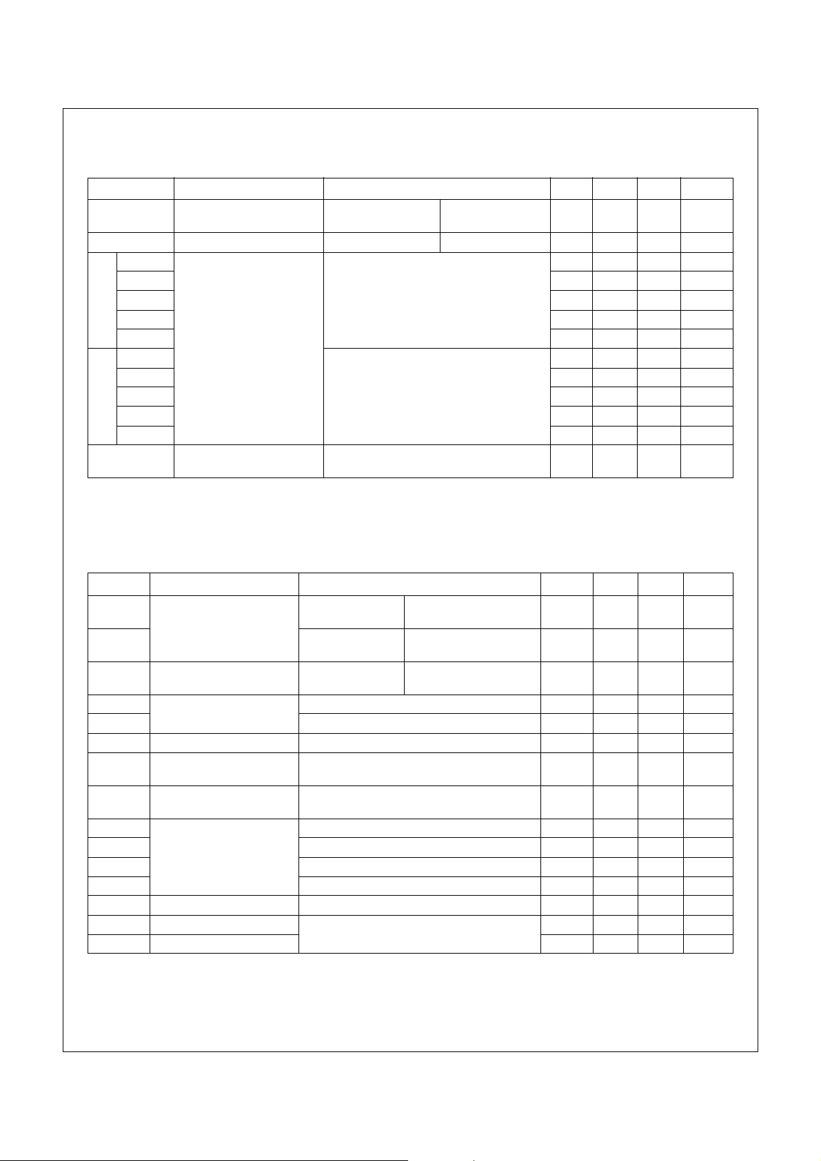
Electrical Characteristics (T
= 25°C, Unless Otherwise Specified)
J
Inverter Part
Symbol Parameter Conditions Min. Typ. Max. Units
V
CE(SAT)
V
F
HS t
t
C(ON)
t
t
C(OFF)
LS t
t
C(ON)
t
t
C(OFF)
I
CES
Note:
3. tON and t
OFF
For the detailed information, please see Figure 4.
Collector-Emitter Saturation
Voltage
VCC = VBS = 15V
V
= 5V
IN
= 5A, TJ = 25°C - - 2.0 V
I
C
FWD Forward Voltage VIN = 0V IF = 5A, TJ = 25°C - - 2.1 V
Switching Times VPN = 300V, VCC = VBS = 15V
ON
OFF
I
= 5A
C
V
= 0V ↔ 5V, Inductive Load
IN
(Note 3)
-0.75- μs
-0.15- μs
-0.60- μs
-0.20- μs
t
rr
ON
OFF
VPN = 300V, VCC = VBS = 15V
I
= 5A
C
V
= 0V ↔ 5V, Inductive Load
IN
(Note 3)
-0.10- μs
-0.45- μs
-0.20- μs
-0.60- μs
-0.20- μs
t
rr
Collector-Emitter
VCE = V
Leakage Current
include the propagation delay time of the internal drive IC. t
CES
C(ON)
and t
are the switching time of IGBT itself under the given gate driving condition internally.
C(OFF)
-0.10- μs
--1mA
Control Part
Symbol Parameter Conditions Min. Typ. Max. Units
I
QCCL
I
QCCH
I
QBS
V
FOH
V
V
SC(ref)
TSD Over-temperature protec-
ΔTSD Over-temperature protec-
UV
UV
UV
UV
t
FOD
V
IN(ON)
V
IN(OFF)
Note:
4. Short-circuit current protection is functioning only at the low-sides.
5. The fault-out pulse width t
Quiescent VCC Supply
Current
Quiescent VBS Supply
Current
VCC = 15V
IN
(UL, VL, WL)
VCC = 15V
IN
(UH, VH, WH)
VBS = 15V
IN
(UH, VH, WH)
= 0V
= 0V
= 0V
- COM - - 23 mA
V
CC(L)
- COM - - 600 μA
V
CC(H)
- V
, V
-V
,
V
V
B(U)
B(W)
- V
S(U)
S(W)
B(V)
S(V)
- - 500 μA
Fault Output Voltage VSC = 0V, VFO Circuit: 4.7kΩ to 5V Pull-up 4.5 - - V
FOL
VSC = 1V, VFO Circuit: 4.7kΩ to 5V Pull-up - - 0.8 V
Short Circuit Trip Level VCC = 15V (Note 4) 0.45 0.5 0.55 V
Temperature at LVIC - 160 - °C
tion
Temperature at LVIC - 5 - °C
tion hysterisis
Supply Circuit Under-
CCD
Voltage Protection
CCR
BSD
BSR
Fault-out Pulse Width C
ON Threshold Voltage Applied between IN
OFF Threshold Voltage - - 0.8 V
depends on the capacitance value of C
FOD
Detection Level 10.7 11.9 13.0 V
Reset Level 11.2 12.4 13.4 V
Detection Level 10 11 12 V
Reset Level 10.5 11.5 12.5 V
= 33nF (Note 5) 1.0 1.8 - ms
FOD
, IN
, IN
, IN
,
(UH)
(VH)
(WH)
IN
, IN
(VL)
- COM
(WL)
according to the following approximate equation : C
FOD
(UL)
2.8 - - V
= 18.3 x 10⁻⁶ x t
FOD
FOD
[F]
FSBF5CH60B Rev. C
6 www.fairchildsemi.com
Page 7
100% I
t
rr
C
100% I
FSBF5CH60B Smart Power Module
C
V
IN
t
ON
V
IN(ON)
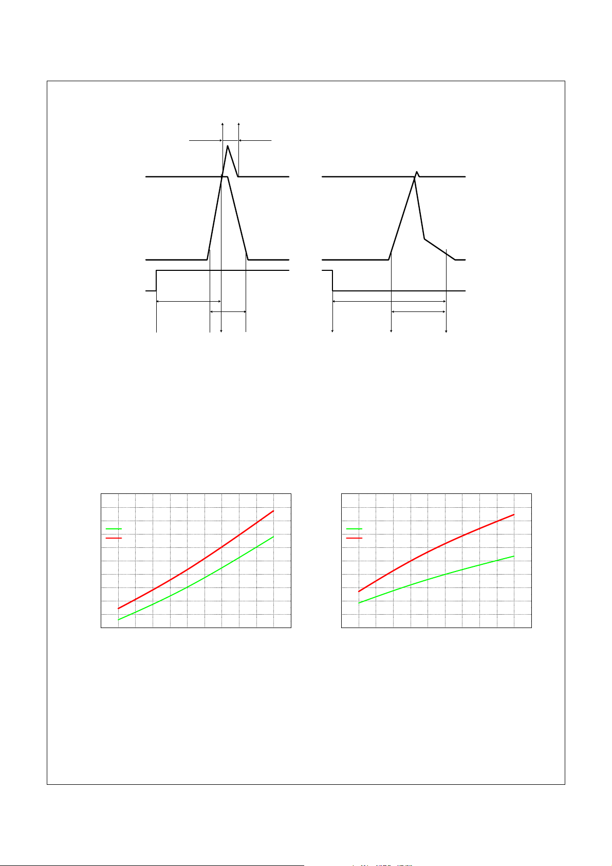
Switching Loss (Typical)
V
CE
10% I
C
t
90% I
C(ON)
10% V
C
I
C
CE
V
(a) turn -o n
Figure 4. Switching Time Definition
IN(OFF)
t
C(OFF)
V
0
10% I
CE
C
I
C
V
IN
t
OFF
10% V
CE
(b) turn -o ff
SWITCHING LOSS(ON) VS. COLLECTOR CURRENT
300
VCE=300V
270
=15V
V
CC
240
V
=5V
[uJ]
IN
TJ=25℃
TJ=150℃
90
60
30
0
0.0 0.5 1.0 1.5 2.0 2.5 3.0 3.5 4.0 4.5 5.0 5.5
SWITCHING LOSS, E
210
SW(ON)
180
150
120
COLLECTOR CURRENT, Ic [AMP ERES ]
Figure 5. Switching Loss Characteristics
SWITCHING LOSS(OFF) VS. COLLECTOR CURRENT
200
VCE=300V
180
=15V
V
CC
160
[uJ]
V
=5V
IN
140
SW(OFF)
120
100
SWITCHING LOSS, E
TJ=25℃
TJ=150℃
80
60
40
20
0
0.0 0.5 1.0 1.5 2.0 2.5 3.0 3.5 4.0 4.5 5.0 5.5
COLLECTOR CURRENT, Ic [AMP ERES ]
FSBF5CH60B Rev. C
7 www.fairchildsemi.com
Page 8
Bootstrap Diode Part
Symbol Parameter Conditions Min. Typ. Max. Units
V
F
t
rr
Forward Voltage IF = 0.1A, TC = 25°C - 2.5 - V
Reverse Recovery Time IF = 0.1A, TC = 25°C - 80 - ns
FSBF5CH60B Smart Power Module
1.0
0.9
0.8
0.7
0.6
0.5
[A]
F
I
0.4
0.3
0.2
0.1
0.0
Note:
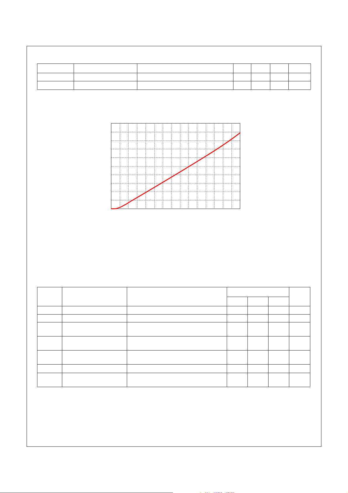
6. Built in bootstrap diode includes around 15Ω resistance characteristic.
Built in Bootstra p Diode VF-IF Characteristic
0123456789101112131415
Figure 6. Built in Bootstrap Diode Characteristics
Recommended Operating Conditions
TC=25℃
VF [V]
Symbol Parameter Conditions
V
V
V
dV
dV
t
dead
f
PWM
V
FSBF5CH60B Rev. C
Supply Voltage Applied between P - NU, NV, N
PN
Control Supply Voltage Applied between V
CC
High-side Bias Voltage Applied between V
BS
/dt,
Control supply variation -1 - 1 V/
CC
/dt
BS
Blanking Time for Preventing
- V
V
B(W)
S(W)
For Each Input Signal 1.5 - - μs
Arm-short
PWM Input Signal -40°C ≤ TC ≤ 125°C, -40°C ≤ TJ ≤ 150°C - - 20 kHz
Voltage for Current Sensing Applied between NU, NV, N
SEN
(Including surge voltage)
Value
Units
Min. Typ. Max.
W
, V
CC(H)
B(U)
- V
- COM 13.5 15 16.5 V
CC(L)
, V
- V
S(U)
W
B(V)
- COM
S(V)
,
8 www.fairchildsemi.com
- 300 400 V
13.0 15 18.5 V
μs
-4 4 V
Page 9
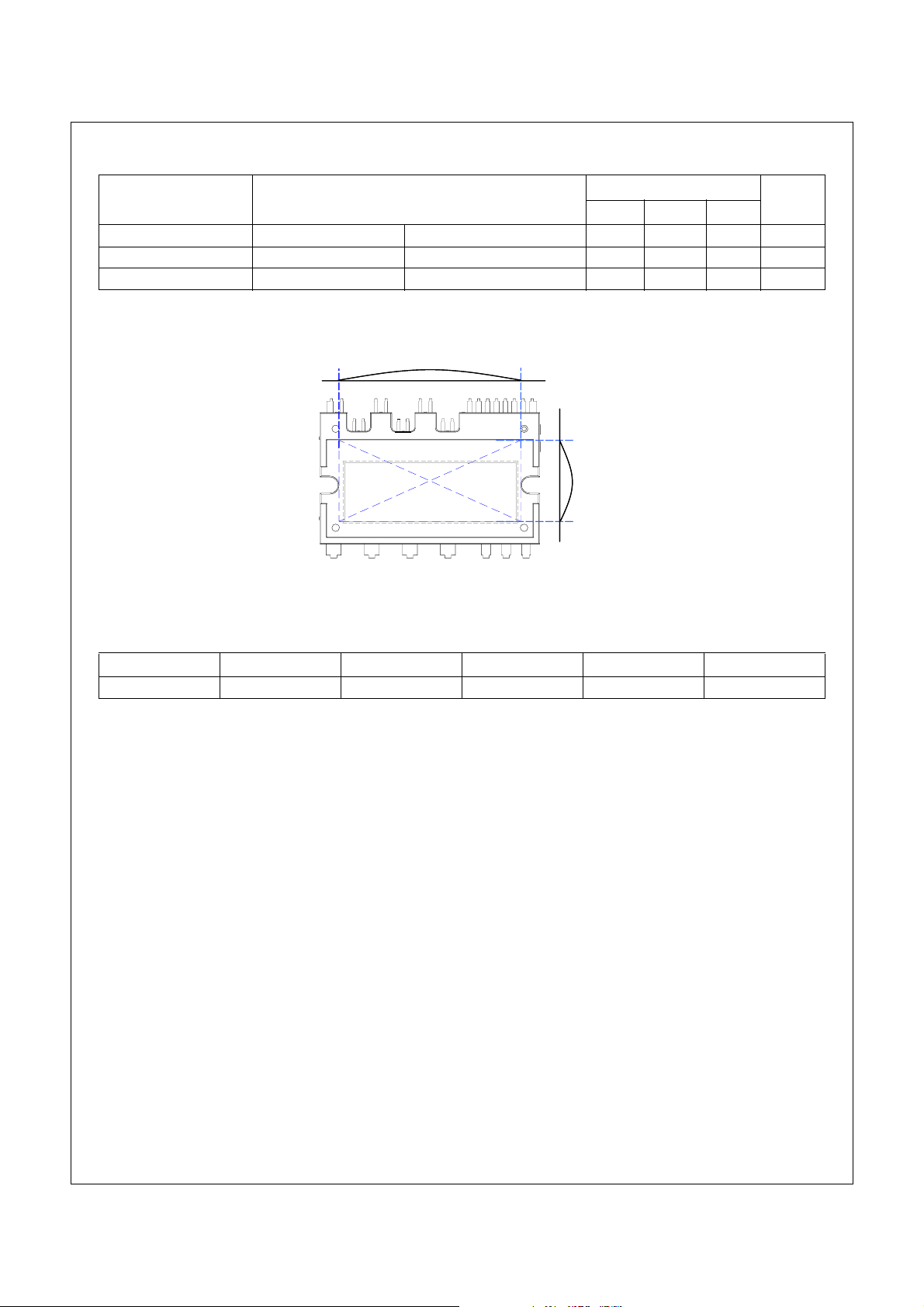
Mechanical Characteristics and Ratings
FSBF5CH60B Smart Power Module
Parameter Conditions
Mounting Torque Mounting Screw: - M3 Recommended 0.62N•m 0.51 0.62 1.00 N•m
Device Flatness Note Figure 7 0 - +120
Weight - 15.4 - g
( + )
( + )
Min. Typ. Max.
( + )
( + )
Limits
Units
Figure 7. Flatness Measurement Position
Package Marking and Ordering Information
μm
Device Marking Device Pack age Reel Size Tape Width Quantity
FSBF5CH60B FSBF5CH60B SPM27-JA - - 10
FSBF5CH60B Rev. C
9 www.fairchildsemi.com
Page 10
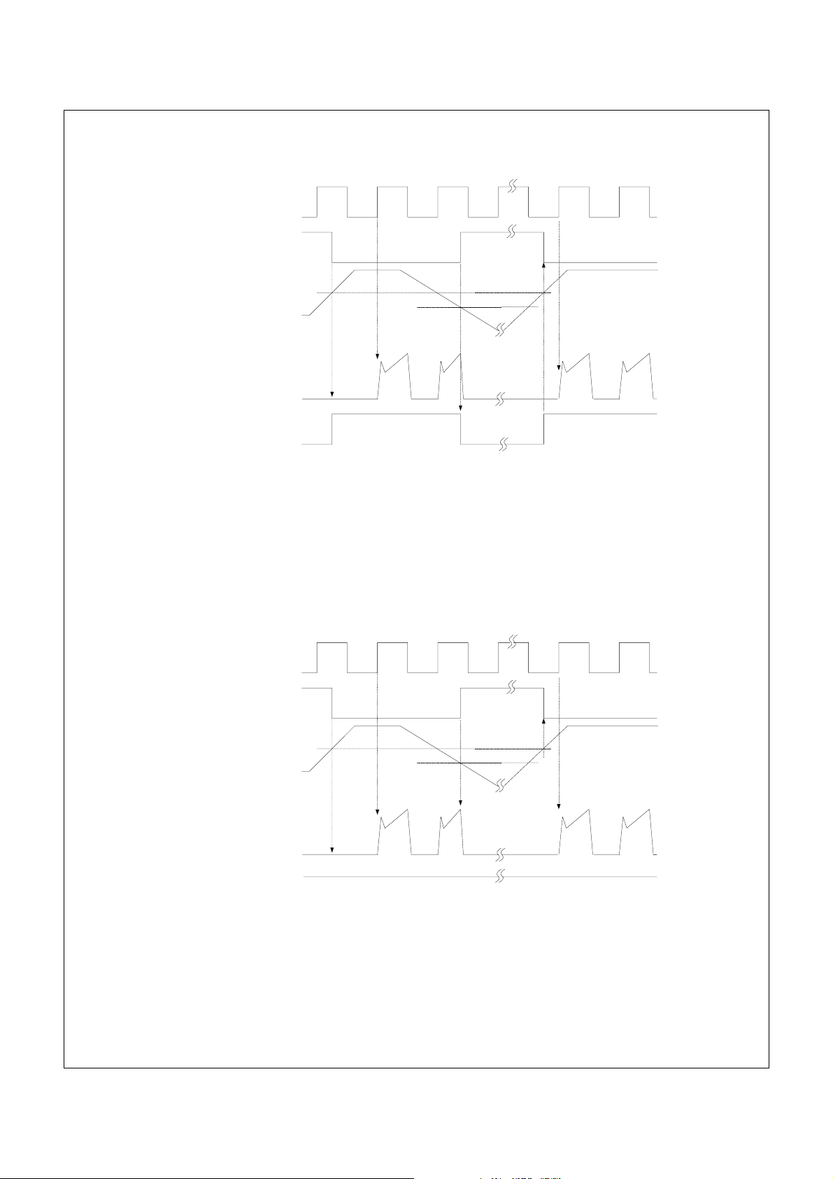
Time Charts of SPMs Protective Function
Input Signal
FSBF5CH60B Smart Power Module
Protection
Circuit State
Control
UV
RESET
CCR
a1
Supply Voltage
Output Current
Fault Output Signal
a1 : Control supply voltage rises: After the voltage rises UV
a2 : Normal operation: IGBT ON and carrying current.
a3 : Under voltage detection (UV
a4 : IGBT OFF in spite of control input condition.
a5 : Fault output operation starts.
a6 : Under voltage reset (UV
a7 : Normal operation: IGBT ON and carrying current.
CCR
CCD
).
).
Figure 8. Under-Voltage Protection (Low-side)
SET RESET
UV
CCD
a3
a2
, the circuits start to operate when next input is applied.
CCR
a4
a5
a6
a7
Input Signal
Protection
Circuit State
Control
Supply Voltage
UV
BSR
RESET
b1
b2
SET RESET
UV
BSD
b3
b4
Output Current
High-level (no fault output)
Fault Output Signal
b1 : Control supply voltage rises: After the voltage reaches UV
b2 : Normal operation: IGBT ON and carrying current.
b3 : Under voltage detection (UV
b4 : IGBT OFF in spite of control input condition, but there is no fault output signal.
b5 : Under voltage reset (UV
b6 : Normal operation: IGBT ON and carrying current
BSR
BSD
)
).
, the circuits start to operate when next input is applied.
BSR
Figure 9. Under-Voltage Protection (High-side)
b5
b6
FSBF5CH60B Rev. C
10 www.fairchildsemi.com
Page 11
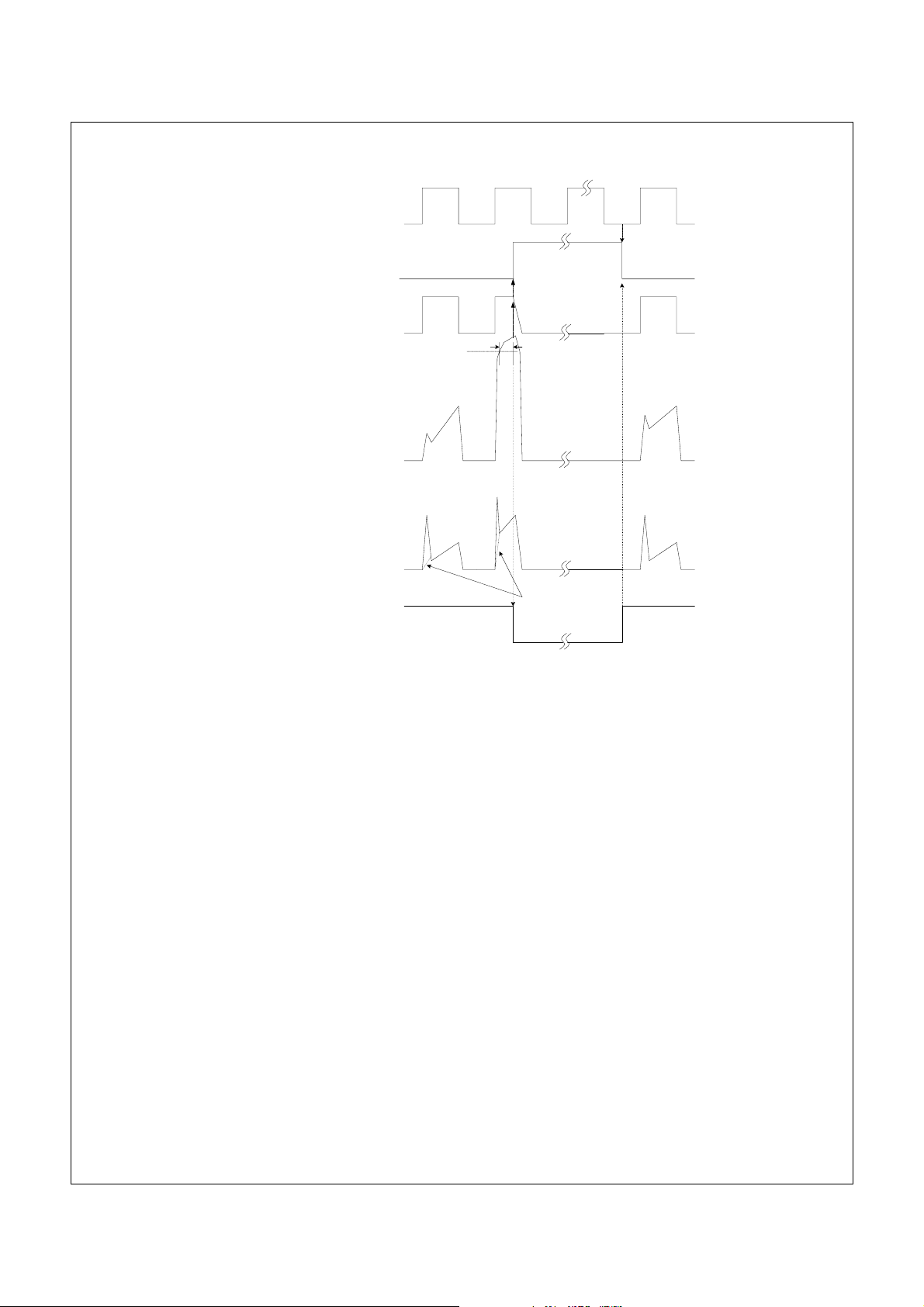
FSBF5CH60B Smart Power Module
Lower arms
control input
Protection
circuit state
Internal IGBT
Gate-Emitter Voltage
Output Current
Sensing Voltage
of the shunt
resistance
Fault Output Signal
c1
SET
c2
SC
c6
c4
c3
SC Reference Voltage
CR circuit time
constant delay
c5
c7
RESET
c8
(with the external shunt resistance and CR connection)
c1 : Normal operation: IGBT ON and carrying current.
c2 : Short circuit current detection (SC trigger).
c3 : Hard IGBT gate interrupt.
c4 : IGBT turns OFF.
c5 : Fault output timer operation starts: The pulse width of the fault output signal is set by the external capacitor C
c6 : Input “L” : IGBT OFF state.
c7 : Input “H”: IGBT ON state, but during the active period of fault output the IGBT doesn’t turn ON.
c8 : IGBT OFF state
Figure 10. Short-Circuit Current Protection (Low-side Operation only)
FO
.
FSBF5CH60B Rev. C
11 www.fairchildsemi.com
Page 12
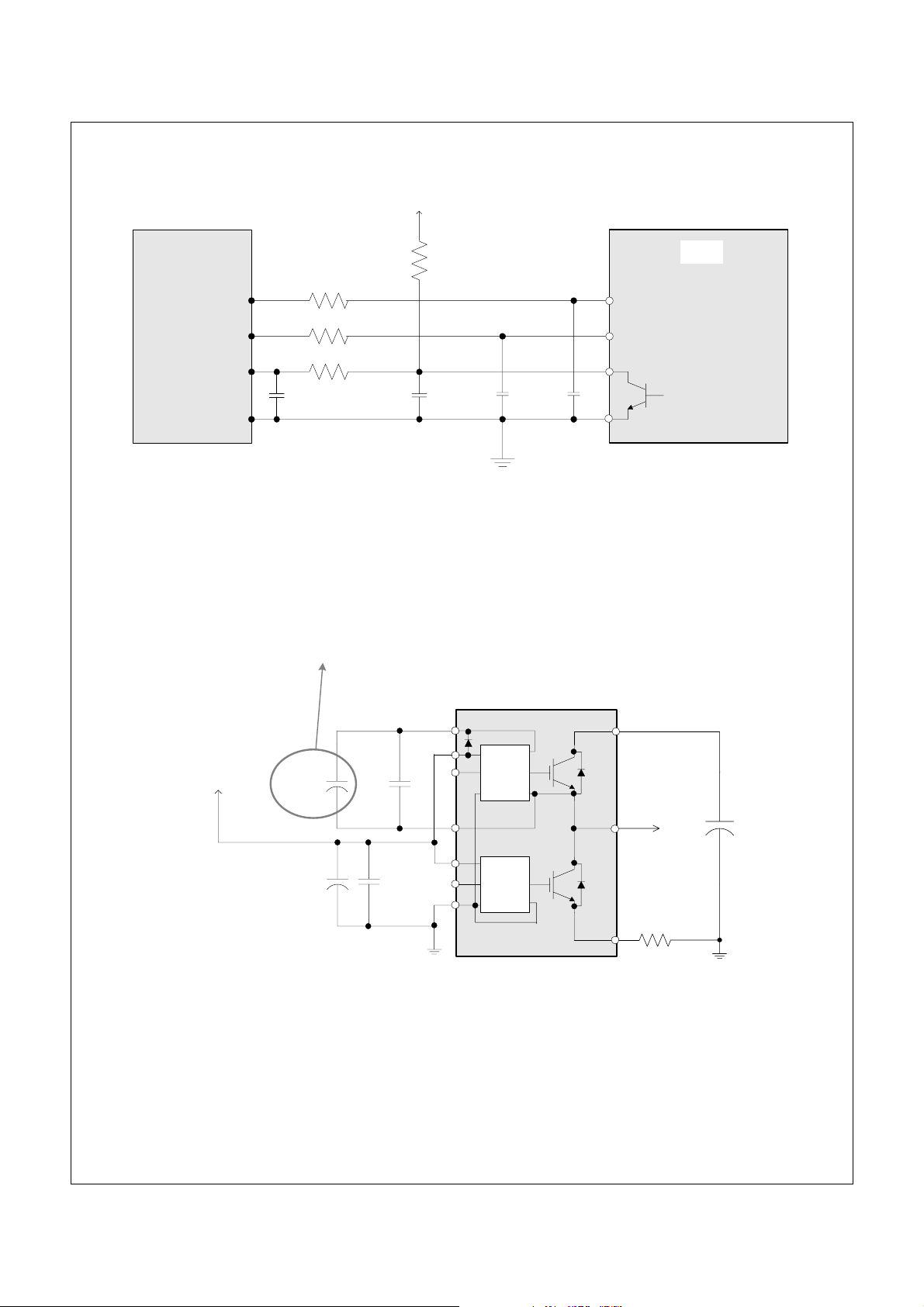
5V-Line
FSBF5CH60B Smart Power Module
R
=4.7㏀
PF
SPM
100Ω
,,
IN
(UH)IN(VH)
IN
(WH)
100Ω
CPU
1nF
100Ω
CPF= 1nF
1nF 1nF
IN
(UL)IN(VL)
V
FO
IN
(WL)
,,
COM
Note:
1) RC coupling at each input might change depending on the PW M contro l scheme use d in the ap plication an d the wiri ng impedan ce of the applica tion’ s printed cir cuit board. The
SPM input signal section integrates 5k
minal.
2) The logic input is compatible with standard CMOS or LSTTL outputs.
Ω (typ.) pull-down resistor . Ther efore, w hen using a n exter nal filtering resistor, please pay attention to the signal volt age drop at inpu t ter-
Figure 11. Recommended CPU I/O Interface Circuit
These Values depend on PWM Control Algorithm
One-Leg Diagram of SPM
Vcc
VB
IN
15V-Line
22uF
0.1uF
1000uF 1uF
Note:
1) The ceramic capacitor placed between VCC-COM should be over 1uF and mounted as close to the pins of the SPM as possible.
COM
Vcc
IN
COM
HO
VS
OUT
V
SL
P
Figure 12. Recommended Bootstrap Operation Circuit and Parameters
Inverter
Output
N
FSBF5CH60B Rev. C
12 www.fairchildsemi.com
Page 13
C
P
U
R
Gating WH
Gating VH
Gating UH
Fault
Gating WL
Gating VL
Gating UL
S
R
S
R
S
R
S
R
S
R
S
R
S
C
C
BPF
PS
Input Signal for
Short-Circuit Protection
CPSC
FSBF5CH60B Smart Power Module
15V line
5V line
C
C
PS
C
PS
C
PS
R
PF
C
PF
PS
BS
CBSC
C
BS
R
F
C
SC
C
C
SPC15
SP15
(19) V
B(W)
(18) V
CC(H)
C
(17) IN
BSC
BSC
C
BSC
(WH)
(20) V
S(W)
(15) V
B(V)
(14) V
CC(H)
(13) IN
(VH)
(16) V
S(V)
(11) V
B(U)
(10) V
CC(H)
(9) IN
(UH)
(12) V
S(U)
(8) C
SC
(7) C
FOD
C
(6) V
FOD
FO
(5) IN
(WL)
(4) IN
(VL)
(3) IN
(UL)
(2) COM
(1) V
CC(L)
VB
VCC
COM
IN
VB
VCC
COM
IN
VB
VCC
COM
IN
C(SC)
C(FOD)
VFO
IN(W L)
IN(VL)
IN(UL)
COM
VCC
OUT
VS
OUT
VS
OUT
VS
OUT(WL)
OUT(VL)
OUT(UL)
V
SL
W-Phase Current
V-Phase Current
U-Phase Current
P (27)
W (26)
V (25)
U (24)
N
W
N
V
NU (21)
R
FW
R
FV
R
M
C
Vdc
DCS
R
(23)
(22)
FU
SW
R
SV
R
SU
C
FW
C
C
FU
FV
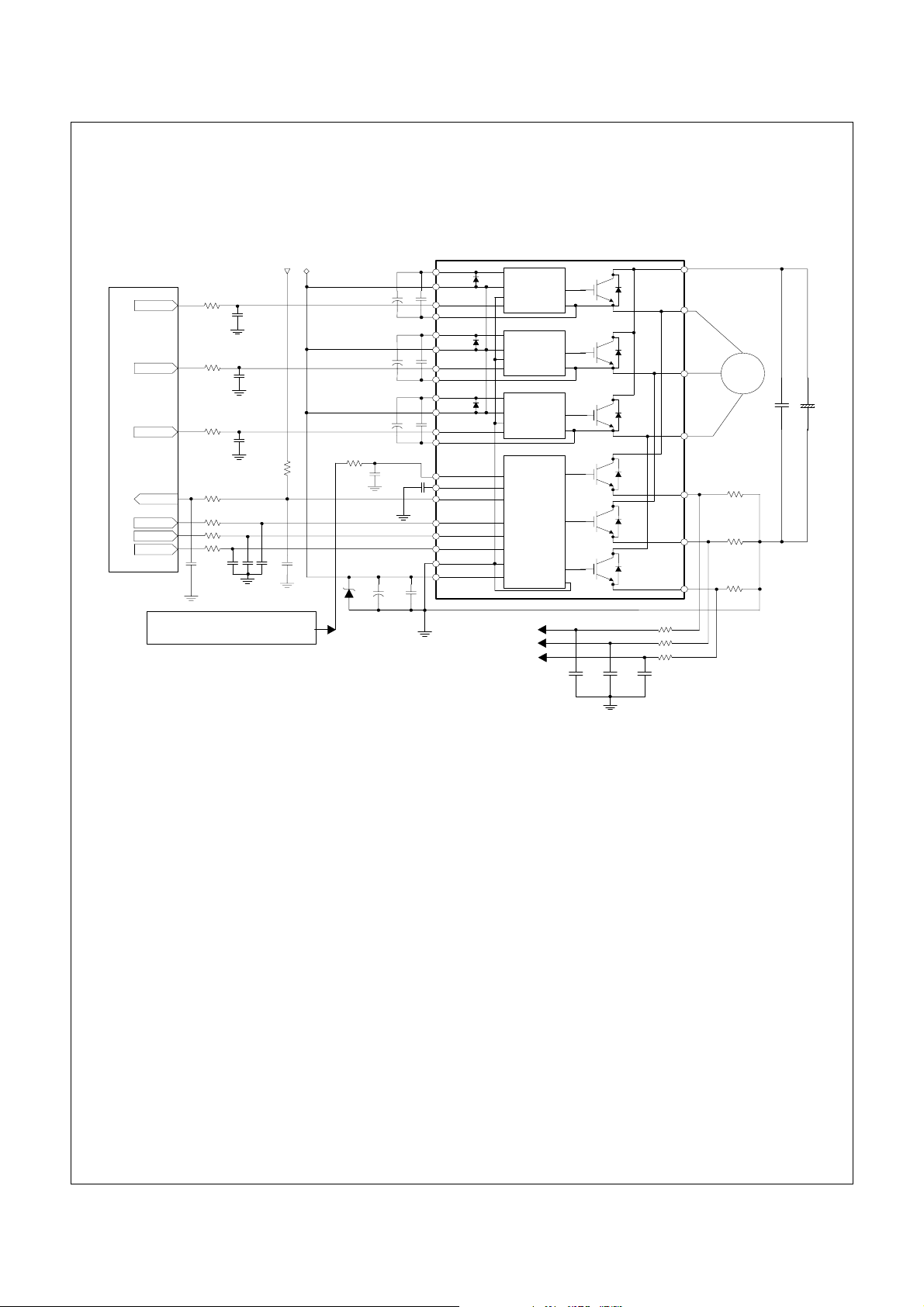
Note:
1) To avoid malfunction, the wiring of each input should be as short as possible. (less than 2-3cm)
2) By virtue of integrating an application specific type HVIC inside the SPM, direct coupling to CPU terminals without any opto-coupler or transformer isolation is possible.
output is open collector type. This signal line should be pulled up to the positive side of the 5V power supply with approximately 4.7kΩ resistance. Please refer to Figure 1 1.
3) V
FO
4) C
of around 7 times larger than bootstrap capacitor CBS is recommended.
SP15
5) V
output pulse width should be determined by connecting an external capacitor(C
FO
(typ.)) Please refer to the note 5 for calculation method.
6) Input signal is High-Active type. There is a 5k
input signal oscillation. R
time constant should be selected in the range 50~150ns. C
SCPS
7) To prevent errors of the protection function, the wiring around R
8) In the short-circuit protection circuit, please select the R
Ω resistor inside the IC to pull down each input signal line to GND. RC coupling circuits should be adopted for the prevention of
and CSC should be as short as possible.
F
time constant in the range 1.5~2μs.
FCSC
) between C
FOD
should not be less than 1nF.(Recommended R
PS
(pin7) and COM(pin2). (Example : if C
FOD
= 33 nF, then tFO = 1.8ms
FOD
=100Ω , CPS=1nF)
S
9) Each capacitor should be mounted as close to the pins of th e SPM as possible.
10) To prevent surge destruction, the wiring betw een the sm oothin g capacitor and the P &GND pins should be as shor t as possi ble. The use of a high frequency non-inductive
capacitor of around 0.1~0.22
μF between the P&GND pins is recommended.
11) Relays are used at almost every systems of electrical equipments of home appliances. In these cases, there should be sufficient distance between the CPU and the relays.
should be over 1μF and mounted as close to the pins of the SPM as possible.
12) C
SPC15
Figure 13. Typical Application Circuit
FSBF5CH60B Rev. C
13 www.fairchildsemi.com
Page 14
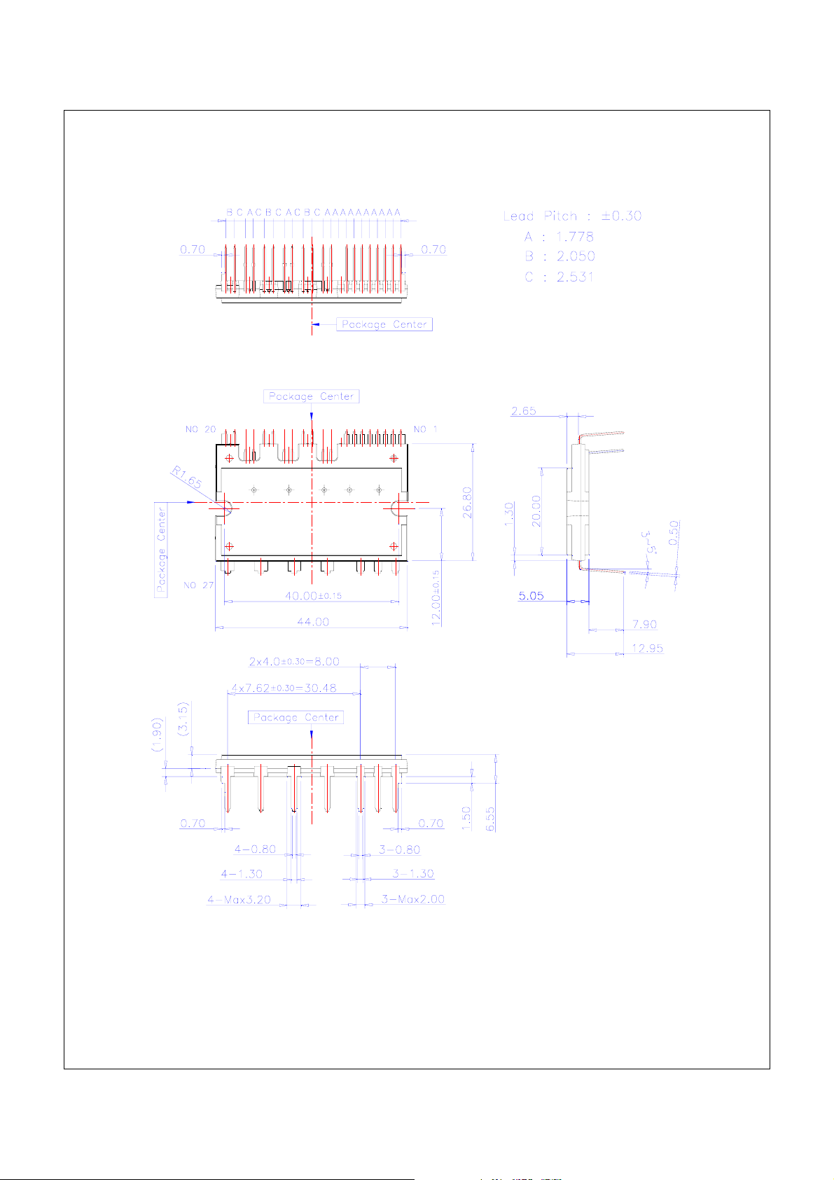
Detailed Package Outline Drawings
FSBF5CH60B Smart Power Module
FSBF5CH60B Rev. C
14 www.fairchildsemi.com
Page 15
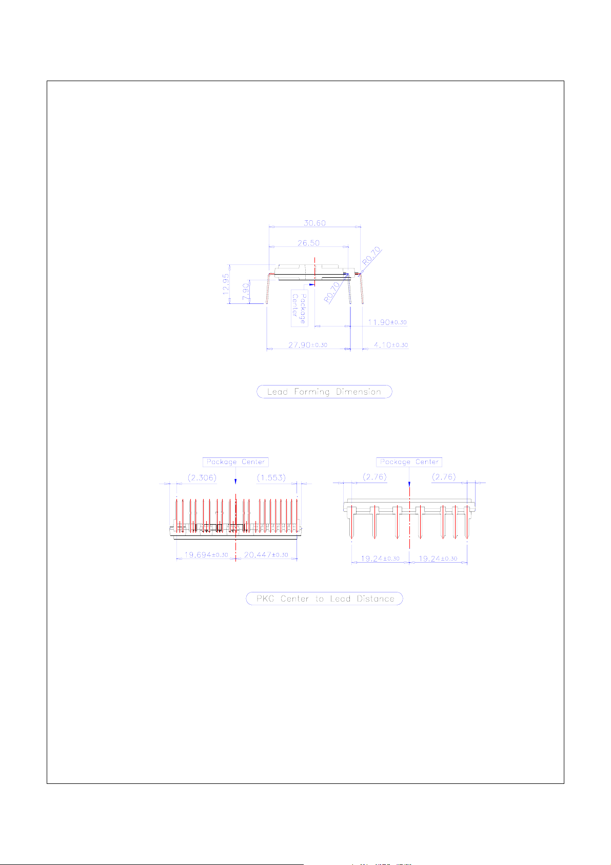
Detailed Package Outline Drawings (Continued)
FSBF5CH60B Smart Power Module
FSBF5CH60B Rev. C
15 www.fairchildsemi.com
Page 16
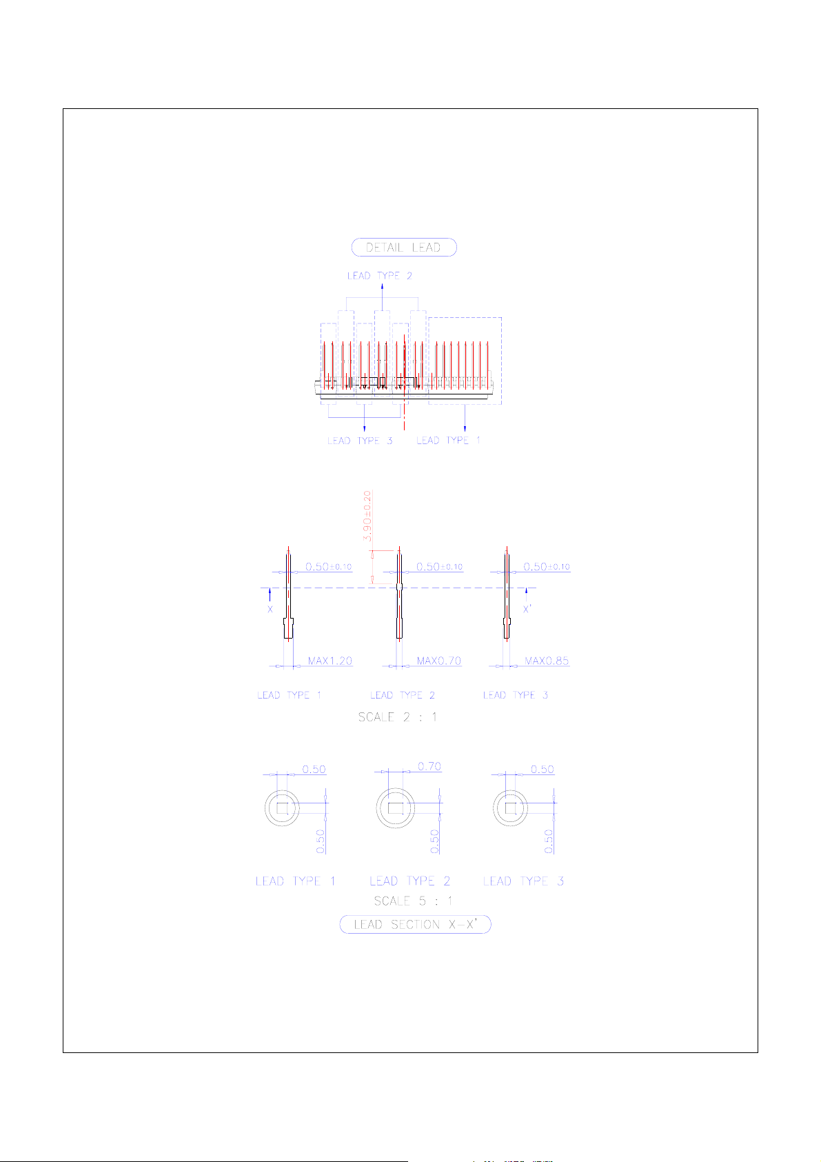
Detailed Package Outline Drawings (Continued)
FSBF5CH60B Smart Power Module
FSBF5CH60B Rev. C
16 www.fairchildsemi.com
Page 17
TRADEMARKS
The following are registered and unregistered trademarks and service marks Fairchild Semiconductor owns or is authorized to use and is not
intended to be an exhaustive list of all such trademarks.
®
ACEx
Build it Now™
CorePLUS™
CROSSVOLT™
CTL™
Current Transfer Logic™
EcoSPARK
FACT Quiet Series™
FACT
FAST
®
®
®
FastvCore™
FPS™
®
FRFET
Global Power ResourceSM
Green FPS™
Green FPS™ e-Series™
GTO™
i-Lo™
IntelliMAX™
ISOPLANAR™
MegaBuck™
MICROCOUPLER™
MicroFET™
MicroPak™
Motion-SPM™
OPTOLOGIC
OPTOPLANAR
PDP-SPM™
Power220
Power247
®
®
®
®
POWEREDGE
Power-SPM™
PowerTrench
Programmable Active Droop™
®
QFET
QS™
QT Optoelectronics™
Quiet Series™
RapidConfigure™
SMART START™
®
SPM
STEALTH™
SuperFET™
SuperSOT™-3
SuperSOT™-6
®
®
SuperSOT™-8
SyncFET™
The Power Franchise
™
TinyBoost™
TinyBuck™
TinyLogic
®
®
TINYOPTO™
TinyPower™
TinyPWM™
TinyWire™
μSerDes™
®
UHC
UniFET™
VCX™
DISCLAIMER
FAIRCHILD SEMICONDUCTOR RESERVES THE RIGHT TO MAKE CHANGES WITHOUT FURTHER NOTICE TO ANY PRODUCTS
HEREIN TO IMPROVE RELIABILITY, FUNCTION, OR DESIGN. FAIRCHILD DOES NOT ASSUME ANY LIABILITY ARISING OUT OF THE
APPLICATION OR USE OF ANY PRODUCT OR CIRCUIT DESCRIBED HEREIN; NEITHER DOES IT CONVEY ANY LICENSE UNDER ITS
PATENT RIGHTS, NOR THE RIGHTS OF OTHERS. THESE SPECIFICATIONS DO NOT EXPAND THE TERMS OF FAIRCHILD’S
WORLDWIDE TERMS AND CONDITIONS, SPECIFICALLY THE WARRANTY THEREIN, WHICH COVERS THESE PRODUCTS.
LIFE SUPPORT POLICY
FAIRCHILD’S PRODUCTS ARE NOT AUTHORIZED FOR USE AS CRITICAL COMPONENTS IN LIFE SUPPORT DEVICES OR
SYSTEMS WITHOUT THE EXPRESS WRITTEN APPROVAL OF FAIRCHILD SEMICONDUCTOR CORPORATION.
As used herein:
1. Life support devices or systems are devices or systems
which, (a) are intended for surgical implant into the body or
(b) support or sustain life, and (c) whose failure to perform
when properly used in accordance with instructions for use
2. A critical component in any component of a life support,
device, or system whose failure to perform can be
reasonably expected to cause the failure of the life support
device or system, or to affect its safety or effectiveness.
provided in the labeling, can be reasonably expected to
result in a significant injury of the user.
PRODUCT STATUS DEFINITIONS
Definition of Terms
Datasheet Identification Product Status Definition
Advance Information Formative or In Design This datasheet contains the design specifications for product
development. Specifications may change in any manner without notice.
Preliminary First Production This datasheet contains preliminary data; supplementary data will be
published at a later date. Fairchild Semiconductor reserves the right to
make changes at any time without notice to improve design.
No Identification Needed Full Production This datasheet contains final specifications. Fairchild Semiconductor
reserves the right to make changes at any time without notice to improve
design.
Obsolete Not In Production This datasheet contains specifications on a product that has been
discontinued by Fairchild Semiconductor. The datasheet is printed for
reference information only.
Rev. I29
© 2007 Fairchild Semiconductor Corporation www.fairchildsemi.com
 Loading...