

Page 1
FS6232
FS6232-01
FS6232FS6232
-01
-01-01
AMERICAN MICROSYSTEMS, INC.
September 2000
1.0 Features
• Generates all clocks required for single and two-way
multi-processor (MP) platforms, including:
M Four differential current-mode Host clock pairs
M Four 66.67MHz 3.3V CK66 clock outputs
M Ten 33.3MHz 3.3V PCI clock outputs
M Two 3.3V Memory Reference clock outputs
M Two 48MHz 3.3V CK48 clock outputs
M Two buffered copies of the crystal reference
• Control of current-mode Host clocks via IREF current
programming pin and ISEL_0:1 current multiplier pins
• Host clock frequency selection via the SEL_A,
SEL_B, and SEL133/100# pins
• Active-low PWR_DWN# signal allows one complete
clock cycle on each clock outputs and then shuts
down the crystal oscillator, PLLs, and outputs
• Spread-spectrum modulation (-0.5% at 31.5kHz) of
SSCG PLL clocks, enabled via SS_EN# input
• Supports test mode and tristate output control to fa-
cilitate board testing
• Available in a 56-pin SSOP and TSSOP
Table 1: Clock Parameters
CLOCK
GROUP#PINS
HOST_P 4 0°
HOST_N 4
MREF_P 1 0°
MREF_N 1
SUPPLY
VOLTAGE
3.3V VDD_H
3.3V VDD_M
SUPPLY
GROUP
FREQ.
(MHz)
133.33
100.00
66.67
50.00
PHASE
180°
180°
CK66 4 3.3V VDD_66 66.67 0° 250ps
PCI 10 3.3V VDD_P 33.33 0° 300ps
CK48 2 3.3V VDD_48 48.008 0° -
REF 2 3.3V VDD_R 14.318 0° -
Table 2: Clock Offsets
RELATION PHASE MIN TYP MAX
CK66 leads PCI 0° 1.5ns 3.5ns
SKEW
(MAX)
150ps
Pair to
Pair
-
Two-Way MP Motherboard Clock Gene rat or IC
Two-Way MP Motherboard Clock Gene rat or IC
Two-Way MP Motherboard Clock Gene rat or ICTwo-Way MP Motherboard Clock Gene rat or IC
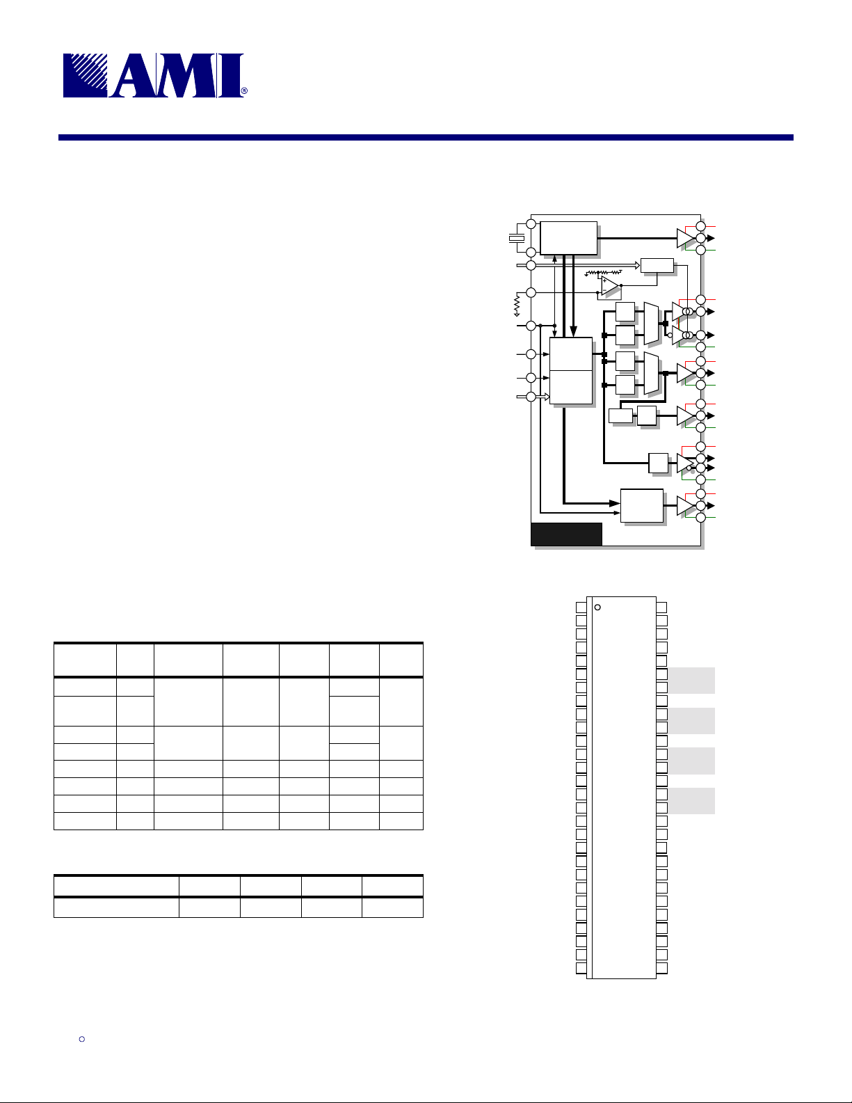
Figure 1: Block Diagram
XIN
XOUT
ISEL_0:1
IREF
PWR_DWN#
SS_EN#
SEL133/100#
SEL_A:B
Crystal
Oscillator
SSCG
PLL
Control
delay
adjust
÷1
÷2
÷3
÷4
÷2
÷4
PLL
VDD_R
REF_0:1
VSS_R
VDD_H
HOST_P1:4
HOST_N1:4
VSS_H
VDD_66
CK66_0:3
VSS_66
VDD_P
PCI_0:9
VSS_P
VDD_M
MREF_P
MREF_N
VSS_M
VDD_48
CK48_0:1
VSS_48
FS6232
Figure 2: Pin Configuration
VSS_R
REF_0 / ISEL_0
REF_1 / ISEL_1
VDD_R
XIN
XOUT
VSS_P
PCI_0
PCI_1
VDD_P
PCI_2
PCI_3
VSS_P
PCI_4
PCI_5
VDD_P
PCI_6
PCI_7
VSS_P
PCI_8
PCI_9
VDD_P
SEL133/100#
VSS_48
CK48_0 / SEL_A
CK48_1 / SEL_B
VDD_48
1
2
3
4
5
6
7
8
9
10
11
12
13
14
15
16
17
18
19
20
21
22
23
24
25
26
27
28
FS6232-01
56
55
54
53
52
51
50
49
48
47
46
45
44
43
42
41
40
39
38
37
36
35
34
33
32
31
30
29
VDD_M
MREF_P
MREF_N
VSS_M
SS_EN#
HOST_P1
HOST_N1
VDD_H
HOST_P2
HOST_N2
VSS_H
HOST_P3
HOST_N3
VDD_H
HOST_P4
HOST_N4
VSS_H
IREF
VDD
VSS
VDD_66
CK66_0
CK66_1
VSS_66
VSS_66
CK66_2
CK66_3
VDD_66PWR_D WN#
Pair 1Pair 2Pair 3Pair 4
Intel and Pentium are registered trademarks of Intel Corporation. Lexmark is a trademark of Lexmark International, Inc. Non-linear spread spectrum modulation profile is licensed under US Patent
No. 5488627, Lexmark International, Inc. This document contains information on a preproduction product. Specifications and information herein are subject to change without notice.
ISO9001
ISO9001
ISO9001ISO9001
9.18.00
IntSKS
Page 2
FS6232-01
FS6232-01
FS6232-01FS6232-01
Two-Way MP Motherboard Clock Gene rat or IC
Two-Way MP Motherboard Clock Gene rat or IC
Two-Way MP Motherboard Clock Gene rat or ICTwo-Way MP Motherboard Clock Gene rat or IC
AMERICAN MICROSYSTEMS, INC.
September 2000
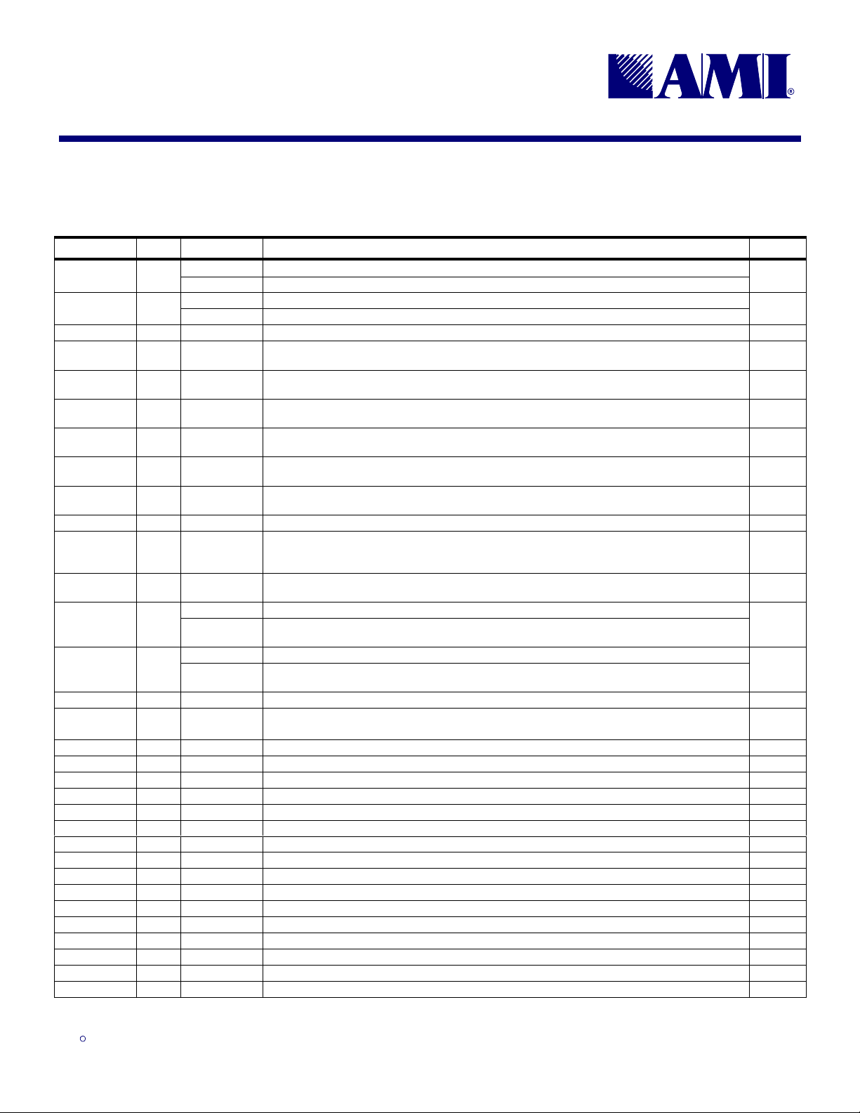
Table 3: Pin Descriptions
Key: AI = Analog Input; AO = Analog Output; DI = Digital Input; DIU = Input with Internal Pull-Up; DID = Input with Internal Pull-Down; DIO = Digital Input/Output; DI-3 = Three-Level Digital Input,
DO = Digital Output; P = Power/Ground; # = Active-low pin
PIN TYPE NAME DESCRIPTION SUPPLY
25 DIO
26 DIO
35, 34, 31, 30 DO CK66_0:3 Four 3.3V 66.67MHz clock outputs, generated from the spread spectrum PLL VDD_66
50, 51 AO
47, 48 AO
44, 45 AO
41, 42 AO
39 AI IREF
54 DO MREF_N
55 DO MREF_P One clock in a pair of outputs provided as a reference clock to a memory clock driver VDD_M
8, 9, 11, 12,
14, 15, 17, 18,
20, 21
28 DI PWR_DWN#
2DIO
3DIO
23 DI SEL133/100# Selects 133MHz (logic high) or 100MHz (logic low) Host clock frequency VDD_48
DO PCI_0:9 Ten 3.3V 33.3MHz PCI clocks, lagging the CK66 clock by 1.5 to 3.5ns VDD_P
CK48_0 One of two 3.3V 48MHz clock outputs, generated from the non-spread PLL
SEL_A One of two latched inputs that select the HOST and MREF output frequency
CK48_1 One of two 3.3V 48MHz clock outputs, generated from the non-spread PLL
SEL_B One of two latched inputs that select the HOST and MREF output frequency
HOST_P1
HOST_N1
HOST_P2
HOST_N2
HOST_P3
HOST_N3
HOST_P4
HOST_N4
REF_0 One of two 3.3V buffered copies of the crystal reference frequency clock
ISEL_0
REF_1 One of two 3.3V buffered copies of the crystal reference frequency clock
ISEL_1
Host clock pair #1; one of six pairs of current-steering differential current-mode outputs. The
current is established via a reference current at IREF and a multiplying factor set by ISEL_0:1
Host clock pair #2; one of six pairs of current-steering differential current-mode outputs VDD_H
Host clock pair #3; one of six pairs of current-steering differential current-mode outputs VDD_H
Host clock pair #4; one of six pairs of current-steering differential current-mode outputs VDD_H
A fixed precision resistor from this pin to ground provides a reference current used for the differential current-mode HOST clock outputs
One clock (180° out of phase with MREF_P) in a pair of outputs provided as a reference clock
to a memory clock driver
Asynchronous active-low LVTTL power-down signal shuts down oscillator and PLL, puts all
clocks in low state. Complete clock cycles on all outputs will occur before shut down begins.
One of two latched inputs that select the multiplying factor of the IREF reference current for the
HOST pair outputs
One of two latched inputs that select the multiplying factor of the IREF reference current for the
HOST pair outputs
VDD_48
VDD_48
VDD_H
VDD
VDD_M
VDD_48
VDD_R
VDD_R
52 DI SS_EN# Active low spread-spectrum enable turns on spread spectrum modulation VDD_M
38 P VDD 3.3V core power supply -
27 P VDD_48 3.3V power supply for CK48 clock outputs 29, 36 P VDD_66 3.3V power supply for CK66 clock outputs 43, 49 P VDD_H 3.3V power supply for the differential HOST clock outputs -
56 P VDD_M 3.3V power supply for MREF clock outputs -
10, 16, 22 P VDD_P 3.3V power supply for PCI clock outputs -
4 P VDD_R 3.3V power supply for the REF clock output and the crystal oscillator 37 P VSS Core ground 24 P VSS_48 Ground for the CK48 clock outputs -
32, 33 P VSS_66 Ground for the CK66 clock outputs
40, 46 P VSS_H Ground for the differential HOST clock outputs -
53 P VSS_M Ground for the MREF clock outputs -
7, 13, 19 P VSS_P Ground for the PCI clock outputs -
1 P VSS_R Ground for the REF clock outputs and the crystal oscillator -
5 AI XIN 14.318MHz crystal oscillator input VDD_R
6 AO XOUT 14.318MHz crystal oscillator output VDD_R
ISO9001
ISO9001
ISO9001ISO9001
2
9.18.00
Page 3
FS6232-01
FS6232-01
FS6232-01FS6232-01
AMERICAN MICROSYSTEMS, INC.
Two-Way MP Motherboard Clock Gene rat or IC
Two-Way MP Motherboard Clock Gene rat or IC
Two-Way MP Motherboard Clock Gene rat or ICTwo-Way MP Motherboard Clock Gene rat or IC
September 2000
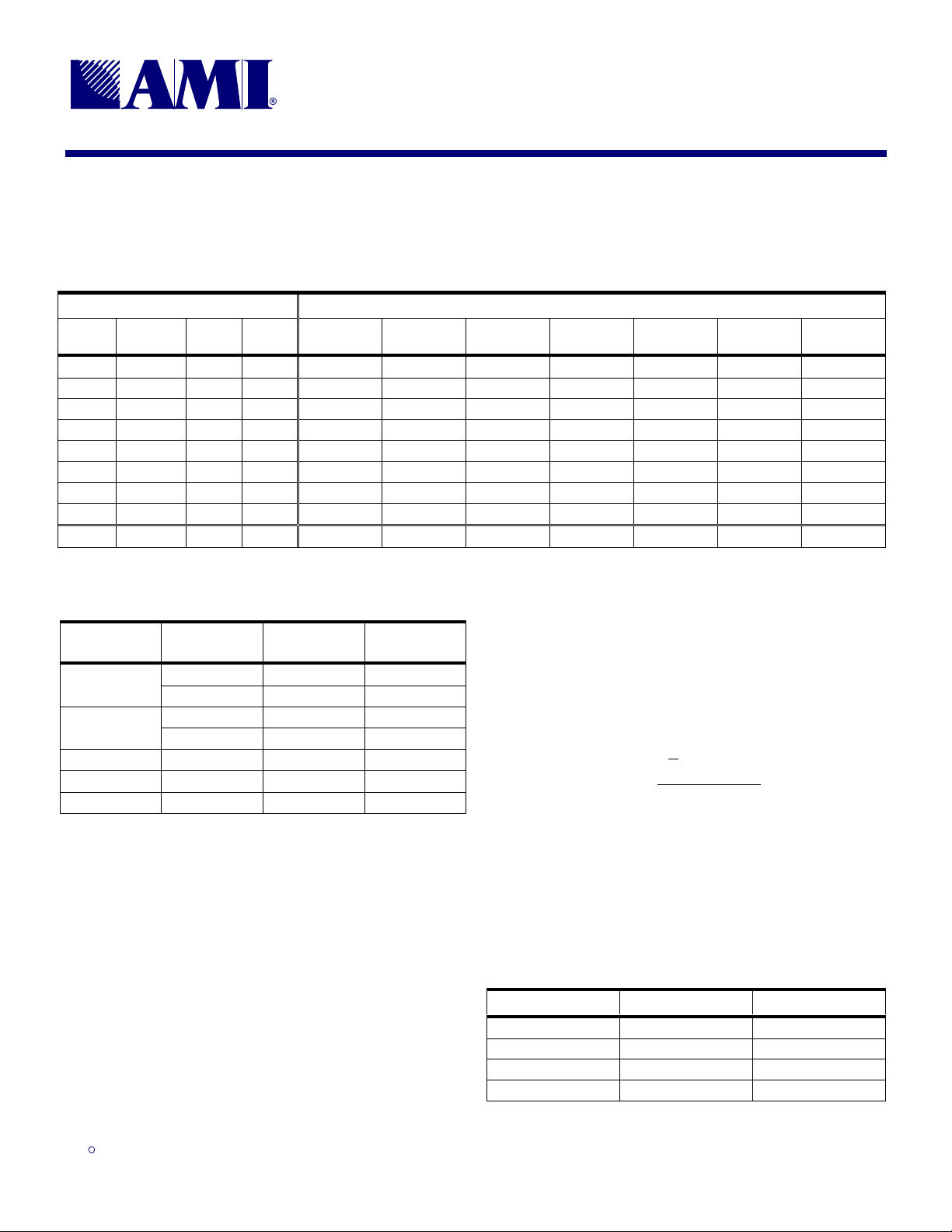
2.0 Programming Information
Table 4: Function/Clock Enable Configuration
CONTROL INPUTS CLOCK OUTPUTS (MHz)
PWR_
DWN#
1 0 0 0 100.00 100.00 50.00 66.67 33.33 48.008 14.318
1 0 0 1 reserved reserved reserved reserved reserved reserved reserved
1 0 1 0 reserved reserved reserved reserved reserved reserved reserved
1 0 1 1 tristate tristate tristate tristate tristate tristate tristate
1 1 0 0 133.33 133.33 66.67 66.67 33.33 48.008 14.318
1 1 0 1 reserved reserved reserved reserved reserved reserved reserved
1 1 1 0 reserved reserved reserved reserved reserved reserved reserved
1 1 1 1 XIN ÷ 2 XIN ÷ 2 XIN ÷ 4 XIN ÷ 4 XIN ÷ 8 XIN ÷ 2 XIN
0XXX
SEL
133/100#
SEL_A SEL_B
HOST_P
1:4
2 × IREF
HOST_N
1:4
tristate low low low low low
MREF_P,
MREF_N
CK66_
0:3
PCI_
0:9
CK48_
0:1
REF
Table 5: Synthesis Error
CLOCK
HOST_P1:4,
HOST_N1:4
MREF_P,
MREF_N
CK66 66.6667 66.6642 -36.657
PCI 33.3333 33.3321 -36.657
(1)
CK48
1. 48MHz USB clock is required to be +167ppm off from 48.000MHz to conform to USB
standards.
2. Spread spectrum is disabled
TARGET
(MHz)
100.0000 99.9963 -36.657
133.3333 133.3072 -195.924
50.0000 49.9982 -36.657
66.6667 66.6536 -195.924
48.000 48.008 +167
ACTUAL
(MHz)
DEVIATION
(ppm)
3.0 HOST Buffer Current Control
The current supplied at the HOST outputs is controlled by
two parameters:
1) the value of the programming resistor from the IREF
pin to ground (VSS), and
2) the multiplier factor determined by the logic setting of
the ISEL_0 and ISEL_1 pins.
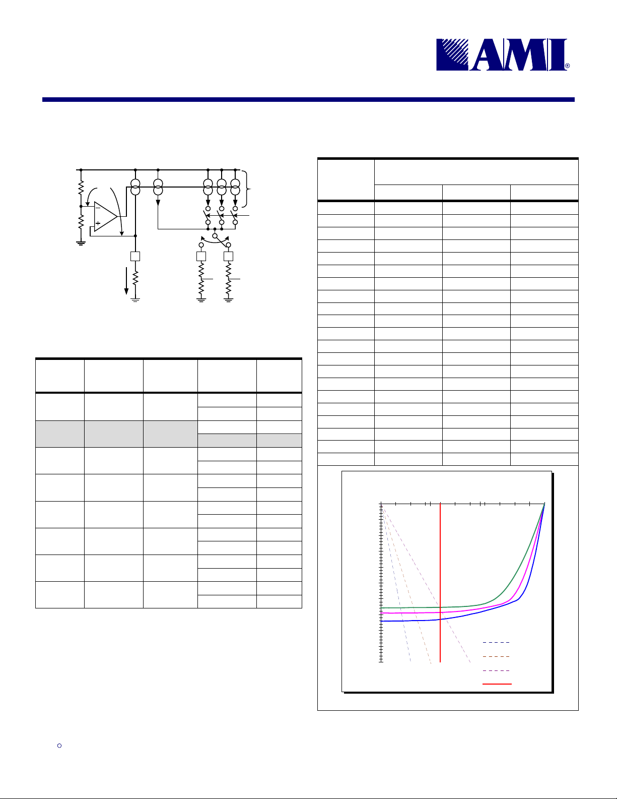
3.1 Current Reference
The HOST output current is a mirrored and scaled copy
of the reference current flowing through the programming
resistor on the IREF pin. Conceptually, the circuit given in
Figure 2 shows how the mirror current is generated.
The voltage that appears at the IREF pin is one-third of
the voltage at the VDD_I pin. The reference current is
1
×=VDD_I
3
REF
R
IREF
I
.
3.2 Current Scaling
The mirrored reference current can be increased by
adding one or more copies of the mirror current together.
The additional current is controlled by the logic settings
on the ISEL_0 and ISEL_1 pins.
Table 6: Current Multiplier
ISEL_0 ISEL_1 MULTPLIER
I
00
01
10
11
= 5 × I
O
I
= 6 × I
O
= 4 × I
I
O
= 7 × I
I
O
REF
REF
REF
REF
ISO9001
ISO9001
ISO9001ISO9001
9.18.00
3
Page 4
FS6232-01
FS6232-01
FS6232-01FS6232-01
Two-Way MP Motherboard Clock Gene rat or IC
Two-Way MP Motherboard Clock Gene rat or IC
Two-Way MP Motherboard Clock Gene rat or ICTwo-Way MP Motherboard Clock Gene rat or IC
AMERICAN MICROSYSTEMS, INC.
September 2000
Figure 2: Current Reference Circuit
VDD_I (3.3V)
2R
1.1V
Mirror
R
IREF
Current
HOST_N
R
S
R
P
R
Reference
Current I
IREF
REF
Table 7: HOST Current Selection
PROGRAM
RESISTOR
R
IREF
475Ω (1%)
475Ω (1%)
475Ω (1%)
475Ω (1%)
221Ω (1%)
221Ω (1%)
221Ω (1%)
221Ω (1%)
NOTE: Shaded row indicates the Primary System Configuration
REFERENCE
CURRENT
I
REF
2.32mA
2.32mA
2.32mA
2.32mA
5mA
5mA
5mA
5mA
CURRENT
MULTIPLIER
I
= 5 × I
O
REF
I
= 6 × I
O
REF
I
= 4 × I
O
REF
I
= 7 × I
O
REF
I
= 5 × I
O
REF
I
= 6 × I
O
REF
I
= 4 × I
O
REF
I
= 7 × I
O
REF
TRACE
IMPEDANCE
60Ω
50Ω
60Ω
50Ω
60Ω
50Ω
60Ω
50Ω
30Ω
25Ω
30Ω
25Ω
30Ω
25Ω
30Ω
25Ω
Additional
Mirror
Current
ISEL_0:1
HOST_P
R
S
R
P
OUTPUT
VOLTAGE
0.71V
0.59V
0.85V
0.71V
0.56V
0.47V
0.99V
0.82V
0.75V
0.62V
0.90V
0.75V
0.60V
0.50V
1.05V
0.84V
Table 8: HOST Buffer Clock Output
Output
Voltage (V)
3.30 0.00 0.00 0.00
3.14 -3.03 -4.22 -5.76
2.97 -5.66 -7.68 -9.86
2.81 -7.87 -10.30 -11.85
2.64 -9.67 -11.91 -12.45
2.48 -11.05 -12.56 -12.84
2.31 -11.98 -12.85 -13.16
2.14 -12.52 -13.07 -13.45
1.98 -12.77 -13.26 -13.72
1.81 -12.91 -13.42 -13.96
1.65 -12.99 -13.54 -14.17
1.48 -13.04 -13.64 -14.36
1.32 -13.07 -13.70 -14.52
1.15 -13.08 -13.73 -14.64
0.99 -13.09 -13.75 -14.71
0.82 -13.11 -13.76 -14.74
0.66 -13.12 -13.78 -14.76
0.49 -13.13 -13.79 -14.78
0.33 -13.13 -13.80 -14.80
0.16 -13.14 -13.81 -14.82
0.00 -13.15 -13.82 -14.83
0123
0
-2
-4
-6
-8
-10
-12
Output Current (mA)
-14
-16
-18
-20
HIGH DRIVE CURRENT (mA)
AT PRIMARY SYSTEM CONFIGURATION
MIN. TYP. MAX.
Output Voltage (V)
30Ω
50Ω
90Ω
Max VOH
ISO9001
ISO9001
ISO9001ISO9001
Data in this table represents nominal characterization data only
9.18.00
4
Page 5
AMERICAN MICROSYSTEMS, INC.
September 2000
FS6232-01
FS6232-01
FS6232-01FS6232-01
Two-Way MP Motherboard Clock Gene rat or IC
Two-Way MP Motherboard Clock Gene rat or IC
Two-Way MP Motherboard Clock Gene rat or ICTwo-Way MP Motherboard Clock Gene rat or IC
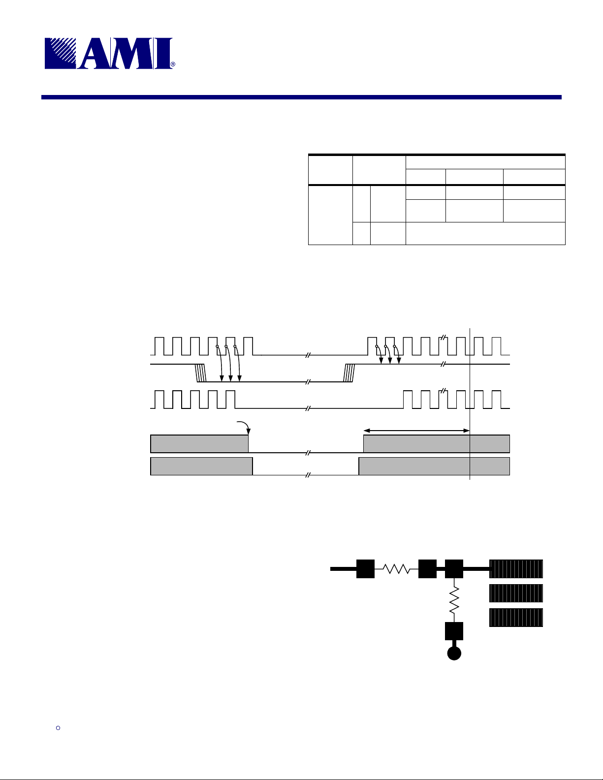
4.0 Power Management
The PWR_DWN# signal is an asynchronous, active-low
LVTTL input that places the device in a low power inactive state without removing power from the device. All
internal clocks are turned off, and all clock outputs are
held low.
Since PWR_DWN# is asynchronous, the signal is synchronized internally to each individual clock. As shown in
Figure 3, a falling-rising-falling edge sequence on any
individual clock output is required before that clock output
is disabled low. This edge sequence ensures that one
complete clock cycle will occur before the clock stops.
Figure 3: PWR_DWN# Timing
Any Clo ck
(internal)
PWR_DWN#
Any Clo ck
(output)
After REF
output shuts off...
Table 9: Latency Table
SIGNAL
PWR_
DWN#
Upon the release of PWR_DWN# (power-up), external
circuitry should allow a minimum of 3ms for the PLL to
lock before enabling any clocks.
SIGNAL
STATE
Power
0
OFF
Power
1
ON
3ms until clock is valid
Output: 2 clocks 3 clocks
Device:
LATENCY
MIN. MAX.
2× REF
clocks
3ms
3× REF clocks
VCO
Crystal
Oscillator
Shaded regions in the Crystal Oscillator and VCO waveforms indicate that the clock is valid and the Crystal Oscillator and VCO are active.
5.0 Dual Function I/O Pins
Several pins on this device serve as dual function input/output pins. During the initial application of VDD to
the device, this type of pin functions as an input pin.
Upon completion of power-up, the logic state present on
the pin is latched internally, and the pin is converted to an
output driver.
An external 10kΩ pull-down resistor to ground is required
for a logic low and a 10kΩ pull-up resistor to the clock
output VDD is required for a logic high. The 10kΩ resistor
presents an insignificant load to the output driver that
should not affect the output clock.
Note that the latching of the logic state occurs only on the
application of the chip supply voltage (VDD). The logic
state on the pin is not latched if the PWR_DWN# signal is
used to power-down the device with VDD still applied.
ISO9001
ISO9001
ISO9001ISO9001
Figure 4: I/O Pin Programming
Termination
Resistor
Clock Trace
5
10k
Programming
Resistor
Ground or
Power Via
Device Solder
Pads
Ω
9.18.00
Page 6
FS6232-01
FS6232-01
FS6232-01FS6232-01
Two-Way MP Motherboard Clock Gene rat or IC
Two-Way MP Motherboard Clock Gene rat or IC
Two-Way MP Motherboard Clock Gene rat or ICTwo-Way MP Motherboard Clock Gene rat or IC
AMERICAN MICROSYSTEMS, INC.
September 2000
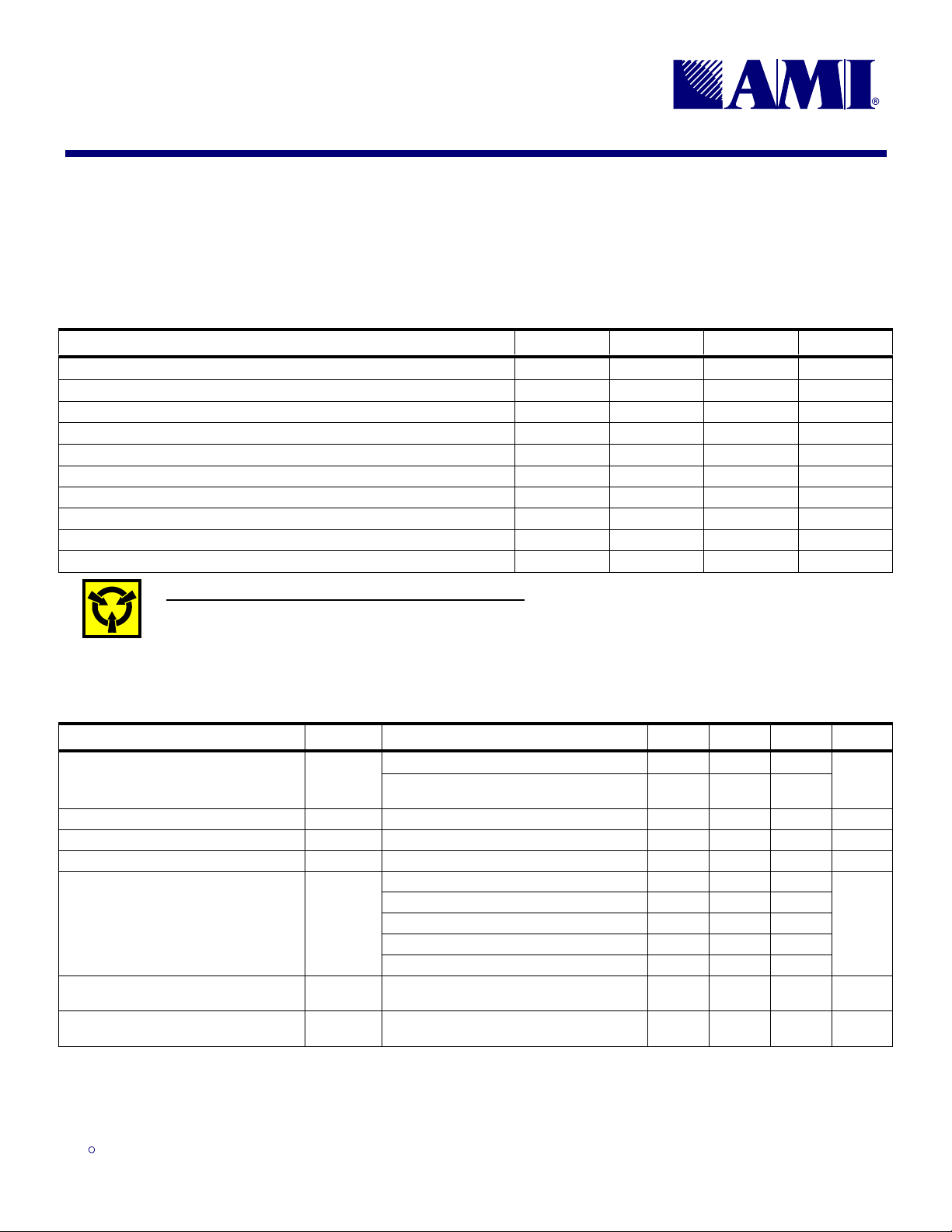
6.0 Electrical Specifications
Table 10: Absolute Maximum Ratings
Stresses above those listed under Absolute Maximum Ratings may cause permanent damage to the device. These conditions represent a stress rating only, and functional operation of the device at
these or any other conditions above the operational limits noted in this specification is not implied. Exposure to maximum rating conditions for extended conditions may affect device performance,
functionality, and reliability.
PARAMETER SYMBOL MIN. MAX. UNITS
Supply Voltage (VSS = ground) V
Input Voltage, dc V
Output Voltage, dc V
Input Clamp Current, dc (VI < 0 or VI > VDD)I
Output Clamp Current, dc (VI < 0 or VI > VDD)I
Storage Temperature Range (non-condensing) T
Ambient Temperature Range, Under Bias T
Junction Temperature T
Lead Temperature (soldering, 10s) 260 °C
Input Static Discharge Voltage Protection (MIL-STD 883E, Method 3015.7) 2 kV
DD
I
O
IK
OK
S
A
J
VSS-0.5 7 V
VSS-0.5 VDD+0.5 V
VSS-0.5 VDD+0.5 V
-50 50 mA
-50 50 mA
-65 150 °C
-55 125 °C
125 °C
CAUTION: ELECTROSTATIC SENSITIVE DEVICE
Permanent damage resulting in a loss of functionality or performance may occur if this device is subjected to a high-energy electrostatic discharge.
Table 11: Operating Conditions
PARAMETER SYMBOL CONDITIONS/DESCRIPTION MIN. TYP. MAX. UNITS
Supply Voltage V
Operating Temperature Range T
Crystal Resonator Frequency f
Crystal Resonator Load Capacitance C
Load Capacitance C
Load Resistance R
Maximum High-Level Output Voltage V
DD
XTAL
OH
Core (VDD) 3.135 3.3 3.465
Clock Buffers (VDD_48, VDD_66, VDD_H,
VDD_M, VDD_P, VDD_R)
A
XL
XIN, XOUT pins 13.5 18 22.5 pF
MREF_P, MREF_N 10 30
PCI_0:9 10 30
CK66_0:3 10 30
L
CK48_0:1 10 20
REF_0:1 10 20
HOST_P1 to HOST_P4,
L
HOST_N1 to HOST_N4
HOST_P1 to HOST_P4,
HOST_N1 to HOST_N4
3.135 3.3 3.465
070°C
14.316 14.318 14.32 MHz
20 105
1.20 V
V
pF
Ω
ISO9001
ISO9001
ISO9001ISO9001
9.18.00
6
Page 7
FS6232-01
FS6232-01
FS6232-01FS6232-01
AMERICAN MICROSYSTEMS, INC.
Two-Way MP Motherboard Clock Gene rat or IC
Two-Way MP Motherboard Clock Gene rat or IC
Two-Way MP Motherboard Clock Gene rat or ICTwo-Way MP Motherboard Clock Gene rat or IC
September 2000
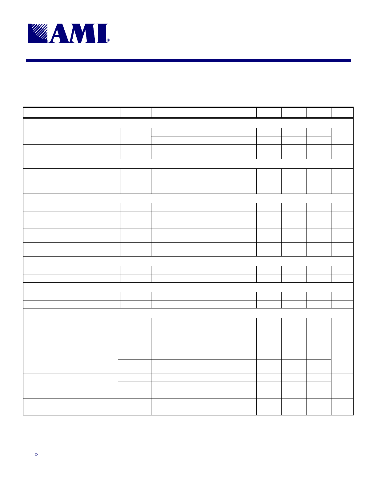
Table 12: DC Electrical Specifications
Unless otherwise stated, all power supplies = 3.3V ± 5%, no load on any output, and ambient temperature range TA = 0°C to 70°C. Parameters denoted with an asterisk ( * ) represent nominal
characterization data and are not currently production tested to any specific limits. MIN and MAX characterization data are ± 3σ from typical. Negative currents indicate current flows out of the device.
PARAMETER SYMBOL CONDITIONS/DESCRIPTION MIN. TYP. MAX. UNITS
Overall
f
=133MHz; VDD=3.465V, R
Supply Current, Dynamic, with Loaded
Outputs
Supply Current, Static I
I
DD
DDs
HOST
f
=100MHz; VDD=3.465V, R
HOST
PWR_DWN# low, all supplies = 3.465V,
R
= 475Ω, IOH = 6 × I
IREF
Digital Inputs (PWR_DWN#, SEL133/100#, SS_EN#)
High-Level Input Voltage V
Low-Level Input Voltage V
Input Leakage Current I
IH
IL
IL
Crystal Oscillator Feedback (XIN)
Threshold Bias Voltage V
High-Level Input Current I
Low-Level Input Current I
Crystal Loading Capacitance * C
Input Loading Capacitance * C
TH
IH
IL
L(xtal)
L(XIN)
VIH = 3.3V 32
VIL = 0V -32
As seen by an external crystal connected to
XIN and XOUT
As seen by an external clock driver on
XOUT; XIN unconnected
Crystal Oscillator Drive (XOUT)
High Level Output Source Current I
Low Level Output Sink Current I
OH
OL
V
= 3.3V, VO = 0V -8.0 mA
I (XIN)
V
= 0V, VO = 3.3V 8.7 mA
I (XIN)
Current Reference (IREF)
Bias Voltage V
Short Circuit Output Source Current I
OH
OH
no load 1.1 V
VO = 0V mA
MREF_P, MREF_N, CK66_0:3, PCI_0:9 Clock Outputs (Type 5 Clock Driver)
VDD_M, VDD_66, VDD_P = 3.135V,
V
= 1.0V
O
VDD_M, VDD_66, VDD_P = 3.465V,
= 3.135V
V
O
VDD_M, VDD_66, VDD_P = 3.135V,
V
= 1.95V
O
VDD_M, VDD_66, VDD_P = 3.465V,
V
= 0.4V
O
Measured at 1.65V, output driving low 12 55
Measured at 1.65V, output driving high 12 55
VO = 0V; shorted for 30s, max. -51 mA
VO = 3.3V; shorted for 30s, max. 62 mA
High Level Output Source Current
I
Low Level Output Sink Current
Output Impedance
Tristate Output Current I
Short Circuit Output Source Current I
Short Circuit Output Sink Current I
I
OH min
OH max
I
OL min
I
OL max
z
z
OZ
OSH
OSL
OL
OH
REF
IREF
IREF
=475Ω, I
=475Ω, I
=6I
OH
REF
=6I
OH
REF
260
250
mA
µA
2.0 VDD+0.3 V
VSS-0.3 0.8 V
-5 +5
µA
1.5 V
µA
µA
13.5 18 22.5 pF
36 pF
-33
mA
-33
30
mA
38
Ω
-10 10
µA
ISO9001
ISO9001
ISO9001ISO9001
9.18.00
7
Page 8
FS6232-01
FS6232-01
FS6232-01FS6232-01
Two-Way MP Motherboard Clock Gene rat or IC
Two-Way MP Motherboard Clock Gene rat or IC
Two-Way MP Motherboard Clock Gene rat or ICTwo-Way MP Motherboard Clock Gene rat or IC
AMERICAN MICROSYSTEMS, INC.
September 2000
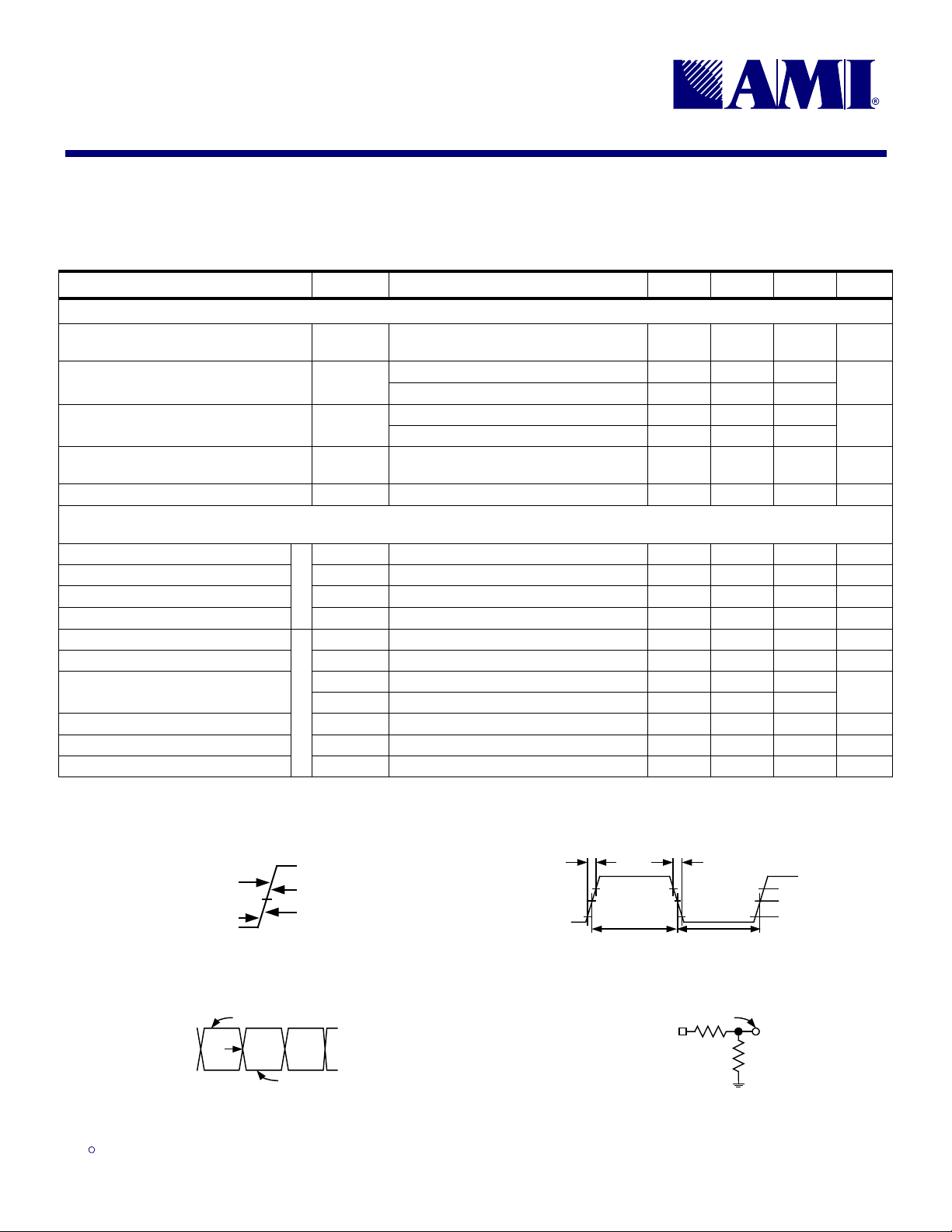
Table 13: DC Electrical Specifications, continued
Unless otherwise stated, all power supplies = 3.3V ± 5%, no load on any output, and ambient temperature range TA = 0°C to 70°C. Parameters denoted with an asterisk ( * ) represent nominal
characterization data and are not currently production tested to any specific limits. MIN and MAX characterization data are ± 3σ from typical. Negative currents indicate current flows out of the device.
PARAMETER SYMBOL CONDITIONS/DESCRIPTION MIN. TYP. MAX. UNITS
HOST_P1:4, HOST_N1:4 Clock Outputs (Type X1 Clock Driver)
R
= 33.2Ω, RP = 49.9Ω,
Crossover Voltage V
High-Level Output Source Current I
Output Source Current Tolerance
Output Impedance z
Tristate Output Current I
X
OH
∆I
OH
OH
OZ
REF_0 / ISEL_0, REF_1 / ISEL_1 Clock Driver I/O, (Type 3)
CK48_0 / SEL_A, CK48_1 / SEL_B Clock Driver I/O (Type 3)
High-Level Input Voltage V
Low-Level Input Voltage V
Input
High-Level Input Current I
Low-Level Input Current (pull-up)
High Level Output Source Current I
Low Level Output Sink Current I
Output Impedance
Output
Tristate Output Current I
Short Circuit Output Source Current I
Short Circuit Output Sink Current
z
z
I
I
OH
OL
OH
OZ
OSH
OSL
IH
IL
IH
IL
OL
S
= 475Ω, IOH = 6 × I
R
IREF
VO = 0.65V, R
VO = 0.74V, R
IREF
IREF
REF
= 475Ω, IOH = 6 × I
= 475Ω, IOH = 6 × I
REF
REF
VDD = 3.3V, over settings in Table 7 -7 +7
VDD_I = 3.3V±5%, over settings in Table 7 -12 +12
∆VO/∆I
, where VO1 = 1.0V, VO2 = VSS,
O
= 475Ω, IOH = 6 × I
R
IREF
REF
45 55 %V
12.9
14.9
3000
-10 10
mA
%I
Ω
µA
2.0 VDD+0.3 V
VSS-0.3 0.8 V
5
VIL = 0.4V -9
µA
µA
VDD_R, VDD_48 = 3.465V, VO = 2.4V -32 mA
VDD_R, VDD_48 = 3.465V, VO = 0.4V 13 mA
Measured at 1.65V, output driving low 20 60
Measured at 1.65V, output driving high 20 60
-10 10
Ω
µA
VO = 0V; shorted for 30s, max. -41 mA
VO = 3.3V; shorted for 30s, max. 40 mA
OH
OH
Figure 5: DC Measurement Diagram
= 3.3V
V
DD
= 2.4V
V
OH
V
OL
= 0.4V
VIH = 2.0V
V
= 0.8V
IL
Figure 7: HOST Clock VX Crossover Point
HOST_P
V
X
HOST_N
ISO9001
ISO9001
ISO9001ISO9001
Figure 6: AC Measurement Diagram
t
r
t
f
d
t
Figure 8: HOST Clock Test Circuit
From output
under test
8
Test node
R
S
R
P
3.3V
2.4V
1.5V
0.4V
9.18.00
Page 9
FS6232-01
FS6232-01
FS6232-01FS6232-01
AMERICAN MICROSYSTEMS, INC.
Two-Way MP Motherboard Clock Gene rat or IC
Two-Way MP Motherboard Clock Gene rat or IC
Two-Way MP Motherboard Clock Gene rat or ICTwo-Way MP Motherboard Clock Gene rat or IC
September 2000
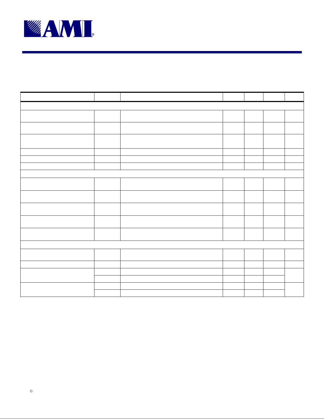
Table 14: AC Timing Specifications
Unless otherwise stated, all power supplies = 3.3V, no load on any output, and ambient temperature TA = 25°C. Parameters denoted with an asterisk ( * ) represent nominal characterization data and
are not currently production tested to any specific limits. MIN and MAX characterization data are ± 3σ fr om typical. Spread spectrum modulation is disabled except for Rise/Fall time measurements.
PARAMETER SYMBOL CONDITIONS/DESCRIPTION MIN. TYP. MAX. UNITS
Overall
Spread Spectrum Modulation
Frequency *
Spread Spectrum Modulation
Index *
Clock Offset t
Output Tristate Enable Delay * t
Output Tristate Disable Delay * t
Power-up PLL Lock Time t
HOST_P1:4, HOST_N1:4 Clock Outputs
Clock Skew * t
Duty Cycle * d
Jitter, Period (peak-peak) *
Rise Time * t
Rise/Fall Time Matching*
MREF_P, MREF_N Clock Output s
Duty Cycle * d
Jitter, Period (peak-peak) *
Rise Time *
Fall Time *
f
m
δ
m
pd
DZL, tDZH
DLZ, tDHZ
L
sk(o)
t
t
j(∆P)
r
t
t
j(∆P)
t
r min
t
r max
t
f min
t
f max
SS_EN# low 31.5 kHz
SS_EN# low -0.5 %
CK66 leads @ 1.5V, CL=30pF to PCI @ 1.5V,
C
= 30pF (measured on rising edges)
L
SEL_A:B = 00, SEL133/100# = 0 1.0 10 ns
SEL_A:B = 11, SEL133/100# = 0 1.0 10 ns
via PWR_DWN# 3.0 ms
HOST pair to HOST pair @ VX, R
= 6 × I
I
OH
Ratio of high pulse width to one clock period at V
R
IREF
Rising edge to rising edge at V
= 6 × I
I
OH
Measured at 20% – 80% of VOH; R
= 6 × I
I
OH
Measured at 20% – 80% of V
= 6 × I
I
OH
Ratio of high pulse width to one clock period,
measured at 1.5V
From rising edge to rising edge at 1.5V, CL=30pF 250 ps
Measured @ 0.4V – 2.4V; CL=10pF 0.4
Measured @ 0.4V – 2.4V; CL=30pF 1.6
Measured @ 2.4V – 0.4V; CL=10pF 0.4
Measured @ 2.4V – 0.4V; CL=30pF 1.6
, R
= 33.2Ω, RP = 49.9Ω
REF
S
= 475Ω, IOH = 6 × I
= 33.2Ω, RP = 49.9Ω
REF RS
= 33.2Ω, RP = 49.9Ω
REF RS
= 33.2Ω, RP = 49.9Ω
REF RS
REF, RS
= 475Ω,
IREF
=33.2Ω, RP=49.9Ω
= 475Ω,
X, RIREF
= 475Ω,
IREF
; R
= 475Ω,
OH
IREF
1.5 3.5 ns
X,
45 55 %
175 450 ps
45 55 %
150 ps
200 ps
20 %
ns
ns
ISO9001
ISO9001
ISO9001ISO9001
9.18.00
9
Page 10
FS6232-01
FS6232-01
FS6232-01FS6232-01
Two-Way MP Motherboard Clock Gene rat or IC
Two-Way MP Motherboard Clock Gene rat or IC
Two-Way MP Motherboard Clock Gene rat or ICTwo-Way MP Motherboard Clock Gene rat or IC
AMERICAN MICROSYSTEMS, INC.
September 2000
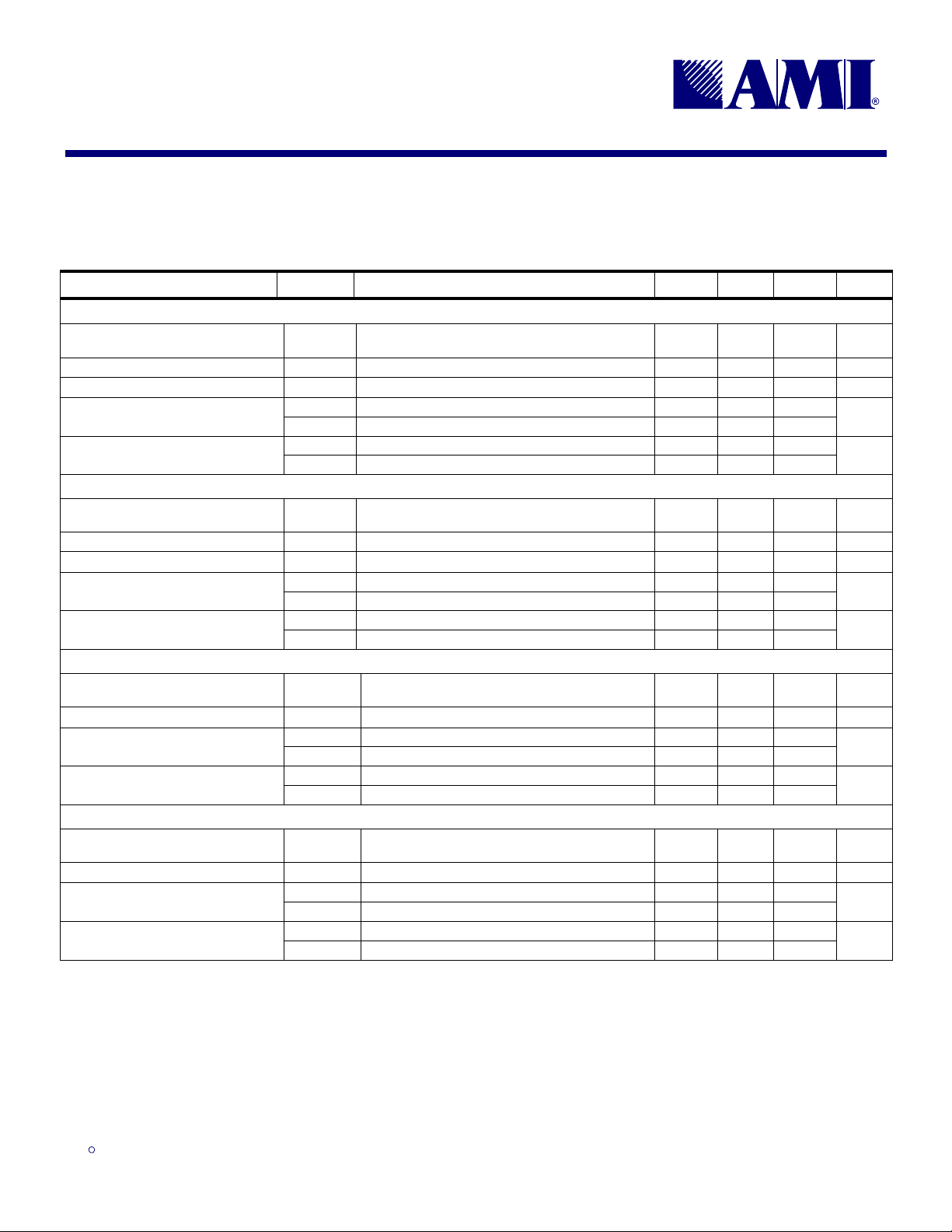
Table 15: AC Timing Specifications, continued
Unless otherwise stated, all power supplies = 3.3V, no load on any output, and ambient temperature TA = 25°C. Parameters denoted with an asterisk ( * ) represent nominal characterization data and
are not currently production tested to any specific limits. MIN and MAX characterization data are ± 3σ fr om typical. Spread spectrum modulation is disabled except for Rise/Fall time measurements.
PARAMETER SYMBOL CONDITIONS/DESCRIPTION MIN. TYP. MAX. UNITS
PCI_0:9 Clock Outputs
Duty Cycle * d
Clock Skew * t
Jitter, Period (peak-peak) *
Rise Time *
Fall Time *
CK66_0:3 Clock Outputs
Duty Cycle * d
Clock Skew * t
Jitter, Period (peak-peak) *
Rise Time *
Fall Time *
REF_0:1 Clock Outputs
Duty Cycle * d
Jitter, Period (peak-peak) *
Rise Time *
Fall Time *
CK48_0:1 Clock Outputs
Duty Cycle * d
Jitter, Period (peak-peak) *
Rise Time *
Fall Time *
t
t
t
t
t
t
t
t
t
t
r max
f max
r max
f max
t
t
t
t
t
t
t
t
t
t
sk(o)
j(∆P)
r min
f min
sk(o)
j(∆P)
r min
f min
j(∆P)
r min
r max
f min
f max
j(∆P)
r min
r max
f min
f max
Ratio of high pulse width to one clock period,
t
measured at 1.5V
One clock output relative to another at 1.5V 500 ps
From rising edge to rising edge at 1.5V, CL = 30pF 500 ps
Measured at 0.4V – 2.4V; CL = 10pF 0.5
Measured at 0.4V – 2.4V; CL = 30pF 2.0
Measured at 2.4V – 0.4V; CL = 10pF 0.5
Measured at 2.4V – 0.4V; CL = 30pF 2.0
Ratio of high pulse width to one clock period,
t
measured at 1.5V
One clock output relative to another at 1.5V 250 ps
From rising edge to rising edge at 1.5V, CL = 30pF 300 ps
Measured at 0.4V – 2.4V; CL = 10pF 0.5
Measured at 0.4V – 2.4V; CL = 30pF 2.0
Measured at 2.4V – 0.4V; CL = 10pF 0.5
Measured at 2.4V – 0.4V; CL = 30pF 2.0
Ratio of high pulse width to one clock period,
t
measured at 1.5V
From rising edge to rising edge at 1.5V, CL = 20pF 1000 ps
Measured at 0.4V – 2.4V; CL = 10pF 1.0
Measured at 0.4V – 2.4V; CL = 20pF 4.0
Measured at 2.4V – 0.4V; CL = 10pF 1.0
Measured at 2.4V – 0.4V; CL = 20pF 4.0
Ratio of high pulse width to one clock period,
t
measured at 1.5V
From rising edge to rising edge at 1.5V, CL = 20pF 350 ps
Measured at 0.4V – 2.4V; CL = 10pF 1.0
Measured at 0.4V – 2.4V; CL = 20pF 4.0
Measured at 2.4V – 0.4V; CL = 10pF 1.0
Measured at 2.4V – 0.4V; CL = 20pF 4.0
45 55 %
ns
ns
45 55 %
ns
ns
45 55 %
ns
ns
45 55 %
ns
ns
ISO9001
ISO9001
ISO9001ISO9001
9.18.00
10
Page 11
AMERICAN MICROSYSTEMS, INC.
Two-Way MP Motherboard Clock Gene rat or IC
Two-Way MP Motherboard Clock Gene rat or IC
Two-Way MP Motherboard Clock Gene rat or ICTwo-Way MP Motherboard Clock Gene rat or IC
September 2000
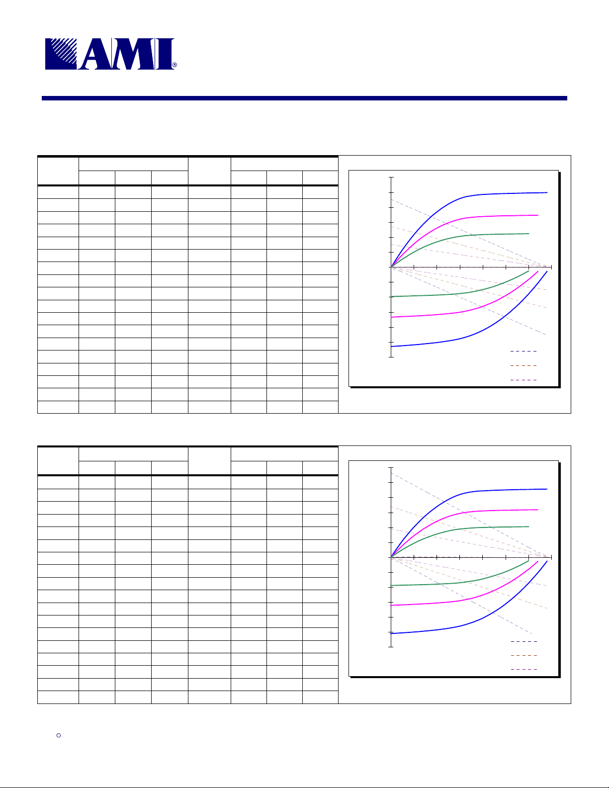
Table 16: MCLK_P, MCLK_N, PCI_0:9, CK66_0:3 Clock Outputs
FS6232-01
FS6232-01
FS6232-01FS6232-01
Voltage
(V)
0 0 0 0 0 -49 -83 -132
0.2 11 17 24 0.2 -48 -83 -131
0.4 21 32 45 0.4 -48 -82 -130
0.6 30 45 64 0.6 -47 -81 -129
0.8 37 56 79 0.8 -47 -80 -127
1.0 43 65 92 1.0 -46 -79 -126
1.2 47 73 103 1.2 -46 -78 -124
1.4 50 78 112 1.4 -45 -76 -121
1.6 53 82 117 1.6 -43 -74 -117
1.8 54 84 120 1.8 -41 -70 -112
2.0 55 85 121 2.0 -37 -65 -105
2.2 55 85 122 2.2 -33 -59 -97
2.4 55 86 123 2.4 -28 -52 -87
2.6 56 86 123 2.6 -22 -43 -74
2.8 56 86 124 2.8 -14 -32 -60
3.0 56 87 124 3.0 -6 -20 -45
3.2 87 124 3.2 -7 -27
3.4 125 3.4 -7
High Drive Current (mA) Low Drive Current (mA)
MIN. TYP. MAX.
Voltage
(V)
MIN. TYP. MAX.
Table 17: REF_0:1, CK48_0:1 Clock Outputs
150
125
100
75
50
25
0
00.511.522.533.5
-25
-50
Output Current (mA)
-75
-100
-125
-150
Output Voltage (V)
Data in this table represents nominal characterization data only
30Ω
50Ω
90Ω
Voltage
(V)
0 0 0 0 0 -38 -64 -102
0.2 8 13 18 0.2 -37 -64 -101
0.4 15 24 33 0.4 -37 -63 -100
0.6 223347 0.6-37-63-99
0.8 274158 0.8-36-62-98
1.0 314868 1.0-36-61-97
1.2 355376 1.2-35-60-95
1.4 375782 1.4-34-59-93
1.6 396086 1.6-33-57-90
1.8 396188 1.8-31-54-87
2.0 406289 2.0-29-50-81
2.2 406390 2.2-25-46-75
2.4 416390 2.4-21-40-67
2.6 416390 2.6-17-33-57
2.8 416391 2.8-11-25-47
3.0 416491 3.0 -5-16-34
3.2 64 91 3.2 -6 -21
3.4 91 3.4 -5
ISO9001
ISO9001
ISO9001ISO9001
High Drive Current (mA) Low Drive Current (mA)
MIN. TYP. MAX.
Voltage
(V)
MIN. TYP. MAX.
11
120
100
80
60
40
20
0
00.511.522.533.5
-20
-40
Output Current (mA)
-60
-80
-100
-120
Output Voltage (V)
Data in this table represents nominal characterization data only
30Ω
50Ω
90Ω
9.18.00
Page 12
FS6232-01
FS6232-01
FS6232-01FS6232-01
Two-Way MP Motherboard Clock Gene rat or IC
Two-Way MP Motherboard Clock Gene rat or IC
Two-Way MP Motherboard Clock Gene rat or ICTwo-Way MP Motherboard Clock Gene rat or IC
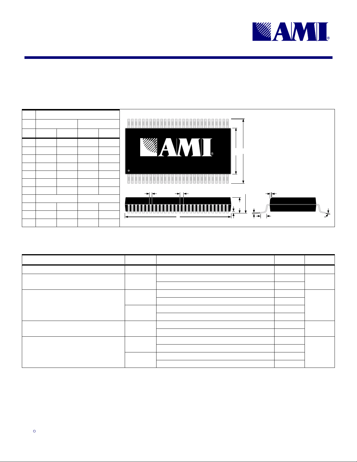
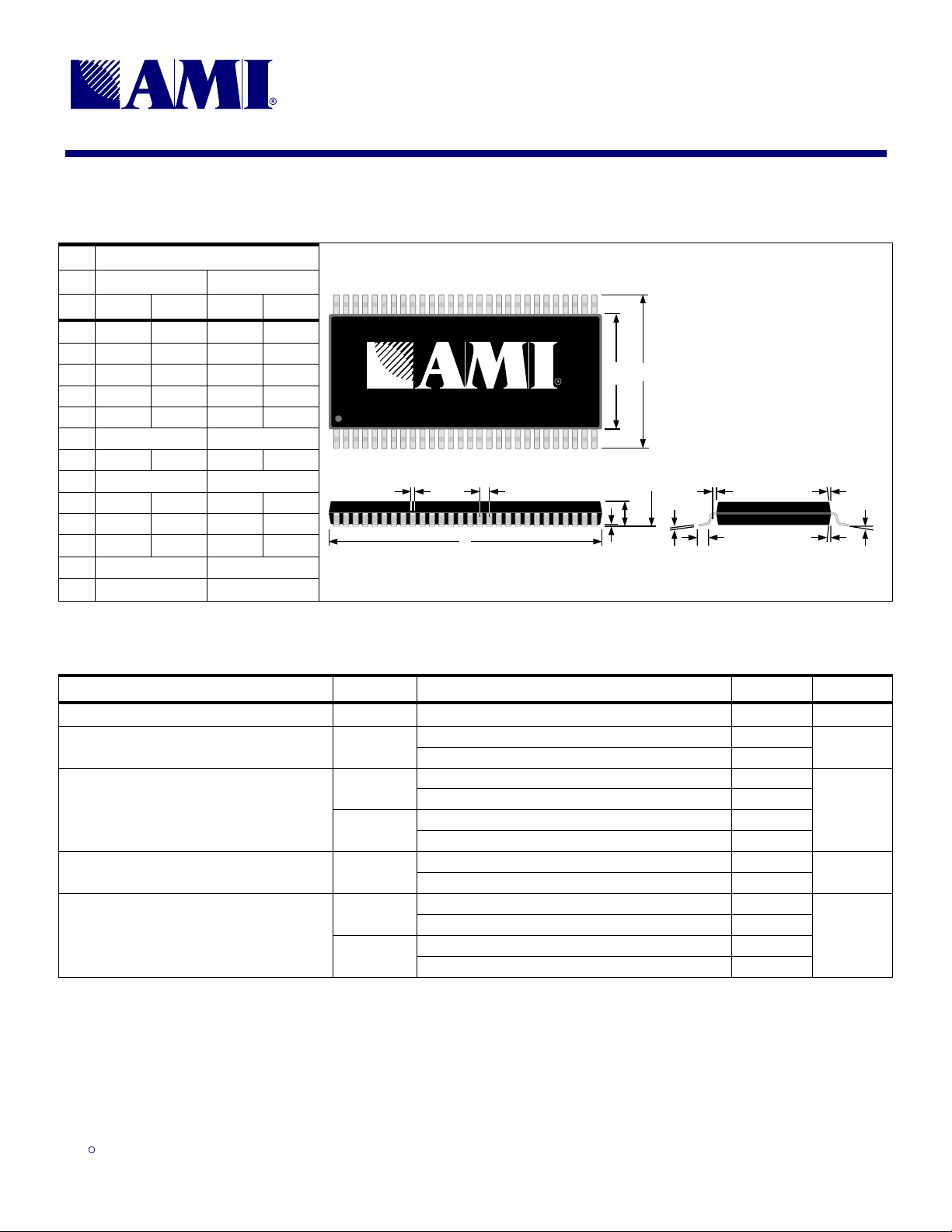
7.0 Package Information
Table 18: 56-pin SSOP (0.300") Package Dimensions
AMERICAN MICROSYSTEMS, INC.
September 2000
DIMENSIONS
INCHES MILLIMETERS
MIN. MAX. MIN. MAX.
A 0.095 0.110 2.41 2.79
A10.008 0.016 0.20 0.41
b 0.008 0.0135 0.20 0.34
c 0.005 0.010 0.13 0.25
D 0.720 0.730 18.29 18.54
E 0.395 0.420 10.03 10.67
E10.291 0.299 7.39 7.59
e 0.025 BSC 0.64 BSC
h 0.015 0.025 0.38 0.64
L 0.020 0.040 0.51 1.01
θ 0° 8° 0° 8°
56
AMERICAN MICROSYSTEMS, INC.
1
b
e
D
Table 19: 56-pin SSOP (0.300") Package Characteristics
PARAMETER SYMBOL CONDITIONS/DESCRIPTION TYP. UNITS
Thermal Impedance, Junction to Free-Air
Lead Inductance, Self L
Lead Inductance, Mutual
Lead Capacitance, Bulk C
Lead Capacitance, Mutual
Θ
JA
11
L
12
L
13
11
C
12
C
13
Air flow = 0 m/s 73 °C/W
Longest trace + wire 6.41
Shortest trace + wire 2.49
Longest trace + wire to first adjacent trace 3.65
Shortest trace + wire to first adjacent trace 1.35
Longest trace + wire to next adjacent trace 2.50
Shortest trace + wire to next adjacent trace 0.90
Longest trace + wire to V
Shortest trace + wire to V
Longest trace + wire to first adjacent trace 0.48
Shortest trace + wire to first adjacent trace 0.20
Longest trace + wire to next adjacent trace 0.07
Shortest trace + wire to next adjacent trace 0.02
SEATING PLANE
SS
SS
E
E
1
h × 45°
A
c
A
1
L
0.94
0.50
θ
nH
nH
pF
pF
ISO9001
ISO9001
ISO9001ISO9001
9.18.00
12
Page 13
AMERICAN MICROSYSTEMS, INC.
Two-Way MP Motherboard Clock Gene rat or IC
Two-Way MP Motherboard Clock Gene rat or IC
Two-Way MP Motherboard Clock Gene rat or ICTwo-Way MP Motherboard Clock Gene rat or IC
September 2000
Table 20: 56-pin TSSOP (6.1mm) Package Dimensions
DIMENSIONS
INCHES MILLIMETERS
MIN. MAX. MIN. MAX.
A - 0.047 - 1.20
A10.002 0.006 0.05 0.15
b 0.0067 0.011 0.17 0.27
c 0.0035 0.008 0.09 0.20
D 0.547 0.555 13.9 14.1
E 0.318 BSC 8.10 BSC
E10.236 0.244 6.00 6.20
e 0.019 BSC 0.50 BSC
L 0.018 0.030 0.45 0.75
S 0.008 - 0.20 -
θ
0° 8° 0° 8°
1
θ
2
θ
3
12° REF 12° REF
12° REF 12° REF
56
AMERICAN MICROSYSTEMS, INC.
1
be
D
E
E
1
SEATING PLANE
A
A
1
FS6232-01
FS6232-01
FS6232-01FS6232-01
c
S
L
θ
θ
2
3
θ
1
Table 21: 56-pin TSSOP (6.1mm) Package Characteristics
PARAMETER SYMBOL CONDITIONS/DESCRIPTION TYP. UNITS
Thermal Impedance, Junction to Free-Air
Lead Inductance, Self L
Lead Inductance, Mutual
Lead Capacitance, Bulk C
Lead Capacitance, Mutual
Θ
JA
11
L
12
L
13
11
C
12
C
13
Air flow = 0 m/s 81 °C/W
Longest trace + wire 4.04
Shortest trace + wire 1.38
Longest trace + wire to first adjacent trace 2.20
Shortest trace + wire to first adjacent trace 0.72
Longest trace + wire to next adjacent trace 1.43
Shortest trace + wire to next adjacent trace 0.48
Longest trace + wire to V
Shortest trace + wire to V
Longest trace + wire to first adjacent trace 0.31
Shortest trace + wire to first adjacent trace 0.07
Longest trace + wire to next adjacent trace 0.04
Shortest trace + wire to next adjacent trace 0.01
nH
nH
SS
SS
0.63
0.21
pF
pF
ISO9001
ISO9001
ISO9001ISO9001
9.18.00
13
Page 14
FS6232-01
FS6232-01
FS6232-01FS6232-01
Two-Way MP Motherboard Clock Gene rat or IC
Two-Way MP Motherboard Clock Gene rat or IC
Two-Way MP Motherboard Clock Gene rat or ICTwo-Way MP Motherboard Clock Gene rat or IC
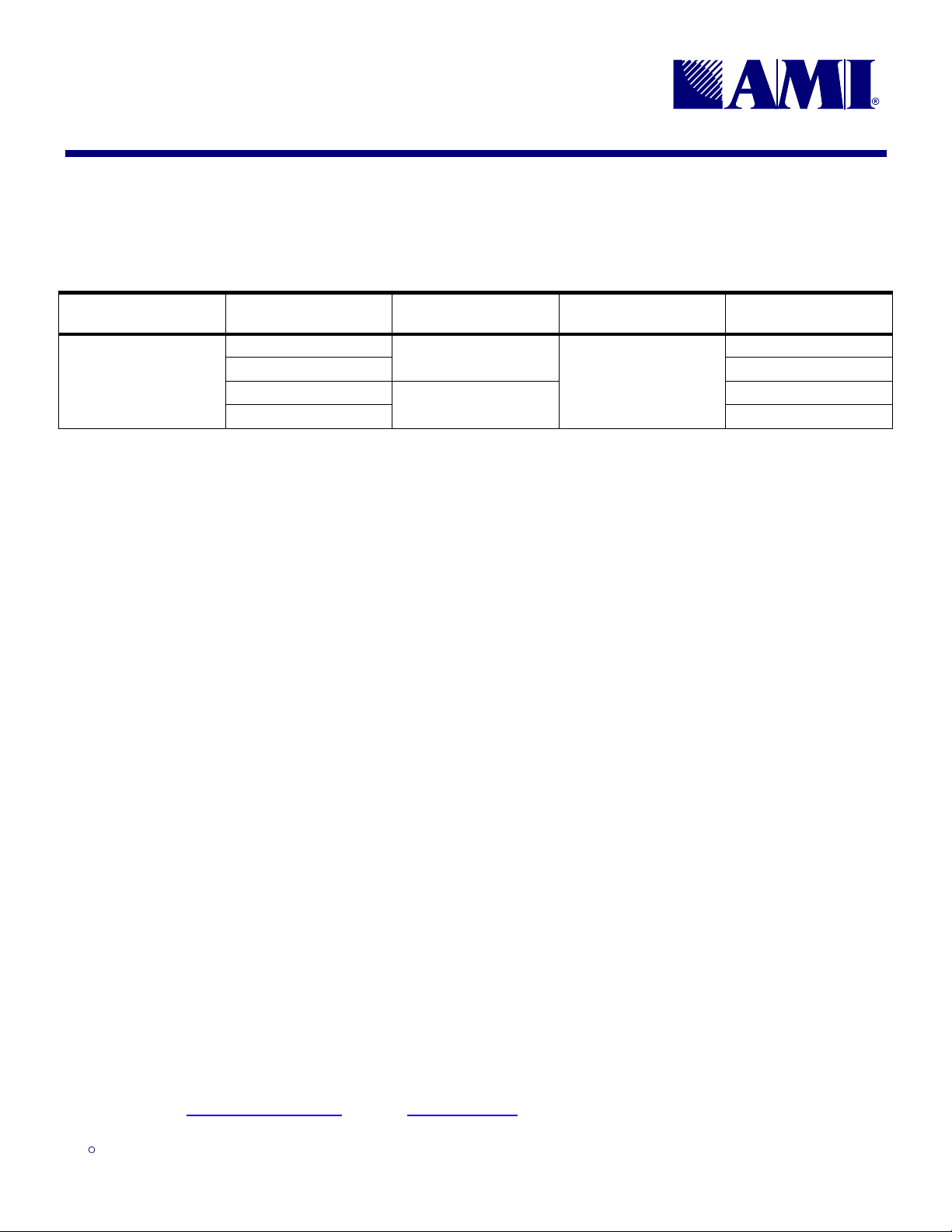
8.0 Ordering Information
Table 22: Device Ordering Codes
AMERICAN MICROSYSTEMS, INC.
September 2000
DEVICE NUMBER ORDERING CODE PACKAGE TYPE
FS6232-01
11995-801
11995-811
11995-201
11995-211
56-pin (0.300”) SSOP
56-pin (6.1mm) TSSOP
OPERATING
TEMPERATURE RANGE
°C to 70°C (Commercial)
0
SHIPPING
CONFIGURATION
Tape and Reel
Tubes
Tape and Reel
Tubes
Copyright © 2000 American Microsystems, Inc.
Devices sold by AMI are covered by the warranty and patent indemnification provisions appearing in its Terms of Sale only. AMI
makes no warranty, express, statutory implied or by description, regarding the information set forth herein or regarding the freedom
of the described devices from patent infringement. AMI makes no warranty of merchantability or fitness for any purposes. AMI reserves the right to discontinue production and change specifications and prices at any time and without notice. AMI’s products are
intended for use in commercial applications. Applications requiring extended temperature range, unusual environmental requirements, or high reliability applications, such as military, medical life-support or life-sustaining equipment, are specifically not recommended without additional processing by AMI for such applications.
American Microsystems, Inc., 2300 Buckskin Rd., Pocatello, ID 83201, (208) 233-4690, FAX (208) 234-6796,
WWW Address: http://www.amis.com E-mail: [email protected]
ISO9001
ISO9001
ISO9001ISO9001
14
9.18.00
 Loading...