

Page 1
FS6128-04 / FS6128-05 / FS6128-06
FS6128-04 / FS6128-05 / FS6128-06
FS6128-04 / FS6128-05 / FS6128-06FS6128-04 / FS6128-05 / FS6128-06
AMERICAN MICROSYSTEMS, INC.
April 2000
1.0 Features
• Phase-locked loop (PLL) device synthesizes output
clock frequency from crystal oscillator or external reference clock
• On-chip tunable voltage-controlled crystal oscillator
(VCXO) allows precise system frequency tuning
• Typically used for generation of MPEG-2 decoder
clock
• 3.3V supply voltage
• Very low phase noise PLL
• Use with “pullable” 14pF crystals – no external pad-
ding capacitors required
• Small circuit board footprint (8-pin 0.150″ SOIC)
• Custom frequency selections available - contact your
local AMI Sales Representative for more information
PLL Clock Generator IC with VCXO
PLL Clock Generator IC with VCXO
PLL Clock Generator IC with VCXOPLL Clock Generator IC with VCXO
2.0 Description
The FS6128 is a monolithic CMOS clock generator IC
designed to minim ize cost a nd com ponen t coun t i n d igital
video/audio systems.
At the core of the FS6128 is circu itry that implements a
voltage-controlle d crystal oscillator (VCXO) when an external resonator (nominally 13.5MHz) is attached. The
VCXO allows device f requenc ies to b e precis el y adjusted
for use in systems that have frequency matching requirements, such as digital satellite receivers.
A high-resolution ph ase-locked loop gener ates an output
clock (CLK) through a pos t-divider. T he CLK f requenc y is
ratiometrically derived from the VCXO frequency. The
locking of the CLK frequency to other system reference
frequencies can el iminate unpredicta ble artifacts in video
systems and reduce electromagnetic interference (EMI)
due to frequency harmonic stacking.
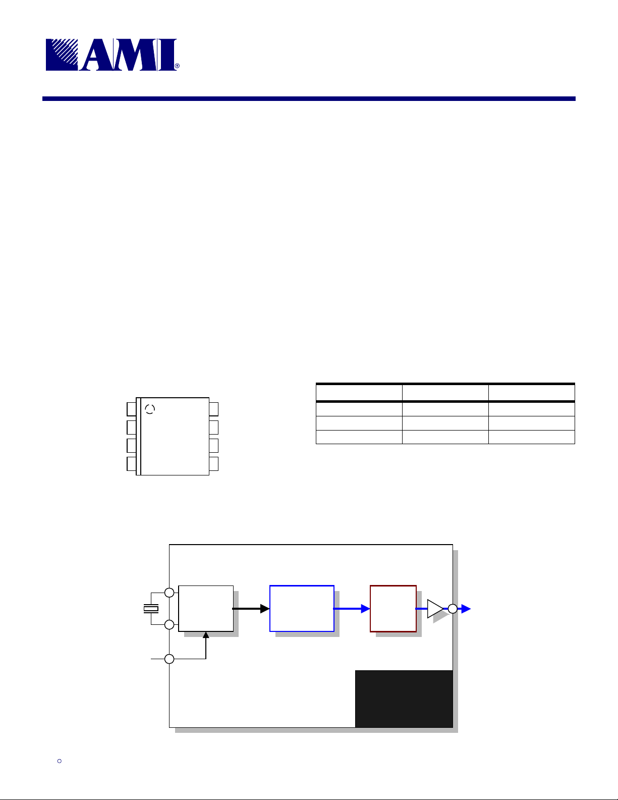
Figure 1: Pin Configuration
1 8
XIN
VDD
XTUNE
VSS
2
3
4
8-pin (0.150″) SOIC
FS6128
Figure 2: Block Diagram
XIN
VCXO
XOUT
XTUNE
7
6
5
XOUT
VSS
n/c
CLK
Table 1: Crystal / Output Frequencies
DEVICE f
FS6128-04 13.500 27.000
FS6128-05 13.500 13.500
FS6128-06 13.500 54.000
NOTE: Contact AMI for custom PLL frequencies
PLL
DIVIDER
(MHz) CLK (M Hz)
XIN
CLK
FS6128-04
FS6128-05
FS6128-06
American Microsystems, Inc. reserves the right to change the detail specifications as may be required to permit improvements in the design of its products.
ISO9001
ISO9001
ISO9001ISO9001
4.24.00
Page 2
FS6128-04 / FS6128-05 / FS6128-06
FS6128-04 / FS6128-05 / FS6128-06
FS6128-04 / FS6128-05 / FS6128-06FS6128-04 / FS6128-05 / FS6128-06
PLL Clock Generator IC with VCXO
PLL Clock Generator IC with VCXO
PLL Clock Generator IC with VCXOPLL Clock Generator IC with VCXO
AMERICAN MICROSYSTEMS, INC.
April 2000
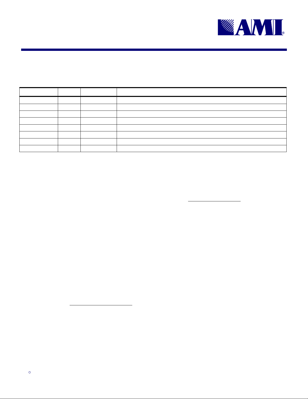
Table 2: Pin Descriptions
Key: AI = Analog Input; AO = Analog Output; DI = Digital Input; DIU = Input with Internal Pull-Up; DID = Input with Internal Pull-Down; DIO = Digital Input/Output; DI-3 = Three-Level Digital Input,
DO = Digital Output; P = Power/Ground; # = Active Low pin
PIN TYPE NAME DESCRIPTION
1 AI XIN VCXO Feedback
2 P VDD Power Supply (+3.3V)
3 AI XTUNE VCXO Tune
4 P VSS Ground
5 DO CLK Cl ock Output
6 - n/c No Connection
7 DO VSS Ground
8 AO XOUT VCXO Drive
3.0 Functional Block Description
3.1 Voltage-Controlled Crystal
Oscillator (VCXO)
The VCXO provides a tunab le, low-jitter frequenc y reference for the rest of the FS6128 system components.
Loading capacitance for the crystal is internal to the
FS6128. No external components (other than the resonator itself) are required for operation of the VCXO.
Continuous fine-tuning of the VCXO f requency is accom plished by varying the voltage on the XTUNE pin. The
value of this voltage controls the effective capacitance
presented to the crystal. The actual amount that this loa d
capacitance change will alter the oscillat or frequency depends on the characteris tics of the crystal as well as the
oscillator circuit itself.
It is important that the cr ystal load capacitance is spec ified correctly to “center” the tuning range. See Table 5.
A simple formula to obtain the “pulling” capability of a
crystal oscillator is:
6
ppmf
)(
=∆
2
where:
C
the shunt (or holder) capacitance of the crystal
0 =
C
the motional capacitance of the crystal
1 =
C
and CL2 = the two extremes (minimum and maximum)
L1
of the applied load capacitance presented by the
FS6128.
()
()()
×−×
CCC
10
LL
121
+×+×
CCCC
LL
1020
EXAMPLE: A crystal with the following parameters is
used: C
and maximum C
range (peak-to-peak) is:
= 0.025pF and C0 = 6pF. Using the minim um
1
f 300
=∆
= 10pF, and CL2 = 20pF, the tuning
L1
()
.
10200250
()()
6
×−×
10
1062062
+×+×
ppm
=
.
3.2 Phase-Locked Loop (PLL)
The on-chip PLL is a standard frequency- and phaselocked loop architecture. The PLL multiplies the r ef er ence
oscillator frequenc y to the desired out put frequency b y a
ratio of integers. The frequency multiplication is exact
with a zero synthesis error (unless otherwise specified).
ISO9001
ISO9001
ISO9001ISO9001
2
4.24.00
Page 3
FS6128-04 / FS6128-05 / FS6128-06
FS6128-04 / FS6128-05 / FS6128-06
FS6128-04 / FS6128-05 / FS6128-06FS6128-04 / FS6128-05 / FS6128-06
AMERICAN MICROSYSTEMS, INC.
PLL Clock Generator IC with VCXO
PLL Clock Generator IC with VCXO
PLL Clock Generator IC with VCXOPLL Clock Generator IC with VCXO
April 2000
4.0 Electrical Specifications
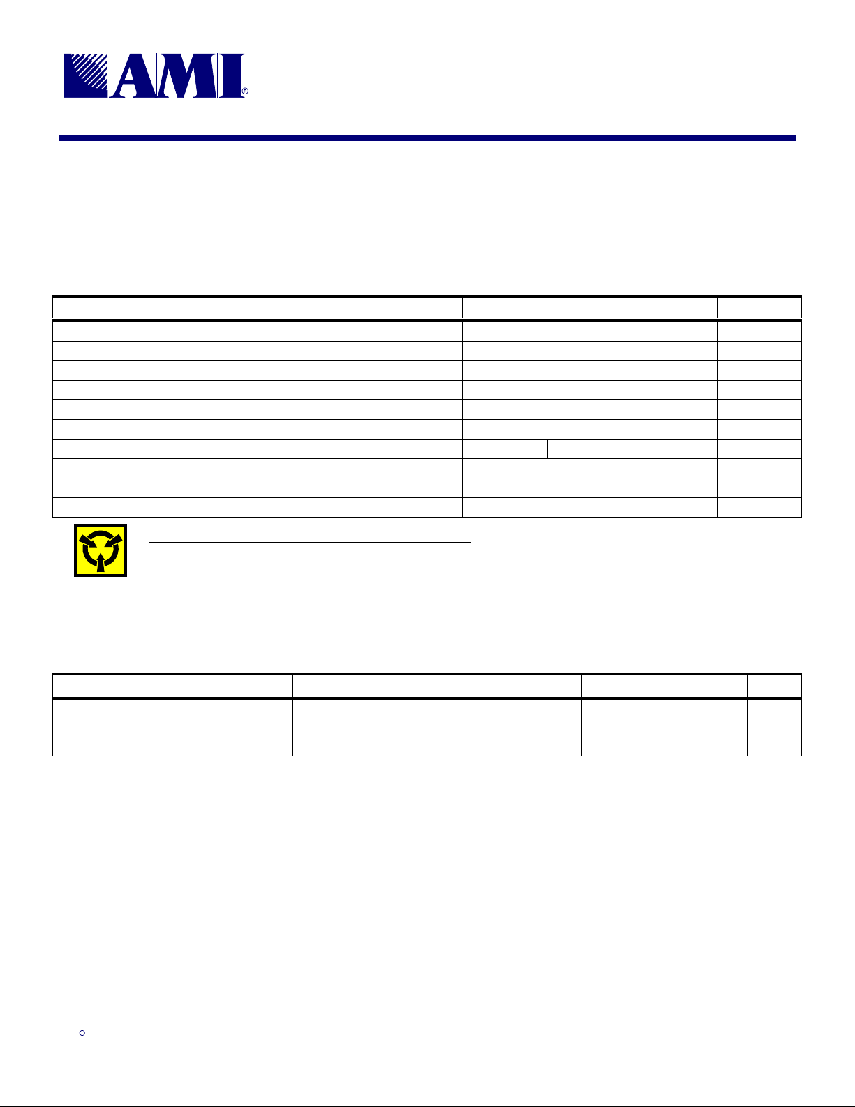
Table 3: Absolute Maximum Ratings
Stresses above those listed under Absolute Maximum Ratings may cause permanent damage to the device. These conditions represent a stress rating only, and functional operation of the device at
these or any other conditions above the operational limits noted in this specification is not implied. Exposure to maximum rating conditions for extended conditions may affect device performance,
functionality, and reliability.
PARAMETER SYMBOL MIN. MAX. UNITS
Supply Voltage (VSS = ground) V
Input Voltage, dc V
Output Voltage, dc V
Input Clamp Current, dc (VI < 0 or VI > VDD)I
Output Clamp Current, dc (VI < 0 or VI > VDD)I
Storage Temperature Range (non-condensing) T
Ambient Temperature Range, Under Bias T
Junction Temperature T
Lead Temperature (soldering, 10s) 260 °C
Input Static Discharge Voltage Protection (MIL-STD 883E, Method 3015.7) 2 kV
DD
I
O
IK
OK
S
A
J
VSS-0.5 7 V
VSS-0.5 VDD+0.5 V
VSS-0.5 VDD+0.5 V
-50 50 mA
-50 50 mA
-65 150 °C
-55 125 °C
125 °C
CAUTION: ELECTROSTATIC SENSITIVE DEVICE
Permanent damage resulting in a loss of functionality or performance may occur if this device is subject ed to a high-energy electrostatic discharge.
Table 4: Operating Conditions
PARAMETER SYMBOL CONDITIONS/DESCRIPTION MIN. TYP. MAX. UNITS
Supply Voltage V
Ambient Operating Temperature Range T
Crystal Resonator Frequency f
DD
XTAL
3.3V ± 10% 3.0 3.3 3.6 V
A
Fundamental Mode 12 13.5 18 MHz
070°C
ISO9001
ISO9001
ISO9001ISO9001
3
4.24.00
Page 4
FS6128-04 / FS6128-05 / FS6128-06
FS6128-04 / FS6128-05 / FS6128-06
FS6128-04 / FS6128-05 / FS6128-06FS6128-04 / FS6128-05 / FS6128-06
PLL Clock Generator IC with VCXO
PLL Clock Generator IC with VCXO
PLL Clock Generator IC with VCXOPLL Clock Generator IC with VCXO
AMERICAN MICROSYSTEMS, INC.
April 2000
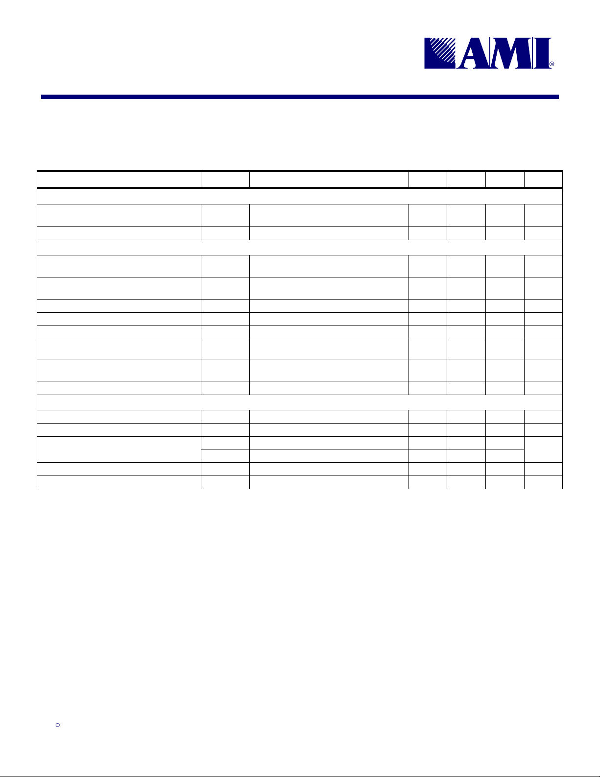
Table 5: DC Electrical Specifications
Unless otherwise stated, VDD = 3.3V ± 10%, no load on any output, and ambient temperature range TA = 0°C to 70°C. Parameters denoted with an asterisk ( * ) represent nominal characterization
data and are not production tested to any specific limits. Where given, MIN and MAX characterization data are ± 3σ from typical. Negative currents indicate current flows out of the device.
PARAMETER SYMBOL CONDITIONS/DESCRIPTION MIN. TYP. MAX. UNITS
Overall
Supply Current, Dynamic, with Loaded
Outputs
Supply Current, Static I
Voltage Controlled Crystal Oscillator (contact factory for approved crystal sources or other application assistance)
Crystal Loading Capacitance at Center
Tuning Voltage
Crystal Resonator Motional Capacitance C
XTUNE Effective Range 03V
Synthesized Load Capacitance Min. C
Synthesized Load Capacitance Max. C
VCXO Tuning Range
VCXO Tuning Characteristic
Crystal Drive Level
Clock Output (CLK)
High-Level Output Source Current * I
Low-Level Output Sink Current * I
Output Impedance *
Short Circuit Source Current * I
Short Circuit Sink Current * I
C
I
DD
DD
L(xtal)
OH
OL
z
OH
z
OL
OSH
OSL
f
= 13.5MHz; CL = 10pF, VDD = 3.6V 30 mA
XTAL
XIN = 0V, VDD = 3.6V 3 mA
Order crystal for this capacitance (parallel
load) at desired center frequency
Specified motional capacitance of the
1
crystal will affect pullability (see text)
L1
L2
@V(XTUNE)=minimum value
@V(XTUNE)=maximum value
f
= 13.5MHz; C
XTAL
(peak-to-peak)
Note: positive change of XTUNE =
positive change of VCXO frequency
R
=20Ω; CL = 20pF
XTAL
VO = 2.0V -40 mA
VO = 0.4V 17 mA
VO = 0.1VDD; output driving high 25
VO = 0.1VDD; output driving low 25
VO = 0V; shorted for 30s, max. -55 mA
VO = 3.3V; shorted for 30s, max. 55 mA
L(xtal)
= 14pF; C
1(xtal)
= 25fF
14 pF
25 fF
10 pF
20 pF
300 ppm
150 ppm/V
200 uW
Ω
ISO9001
ISO9001
ISO9001ISO9001
4
4.24.00
Page 5
FS6128-04 / FS6128-05 / FS6128-06
FS6128-04 / FS6128-05 / FS6128-06
FS6128-04 / FS6128-05 / FS6128-06FS6128-04 / FS6128-05 / FS6128-06
AMERICAN MICROSYSTEMS, INC.
PLL Clock Generator IC with VCXO
PLL Clock Generator IC with VCXO
PLL Clock Generator IC with VCXOPLL Clock Generator IC with VCXO
April 2000
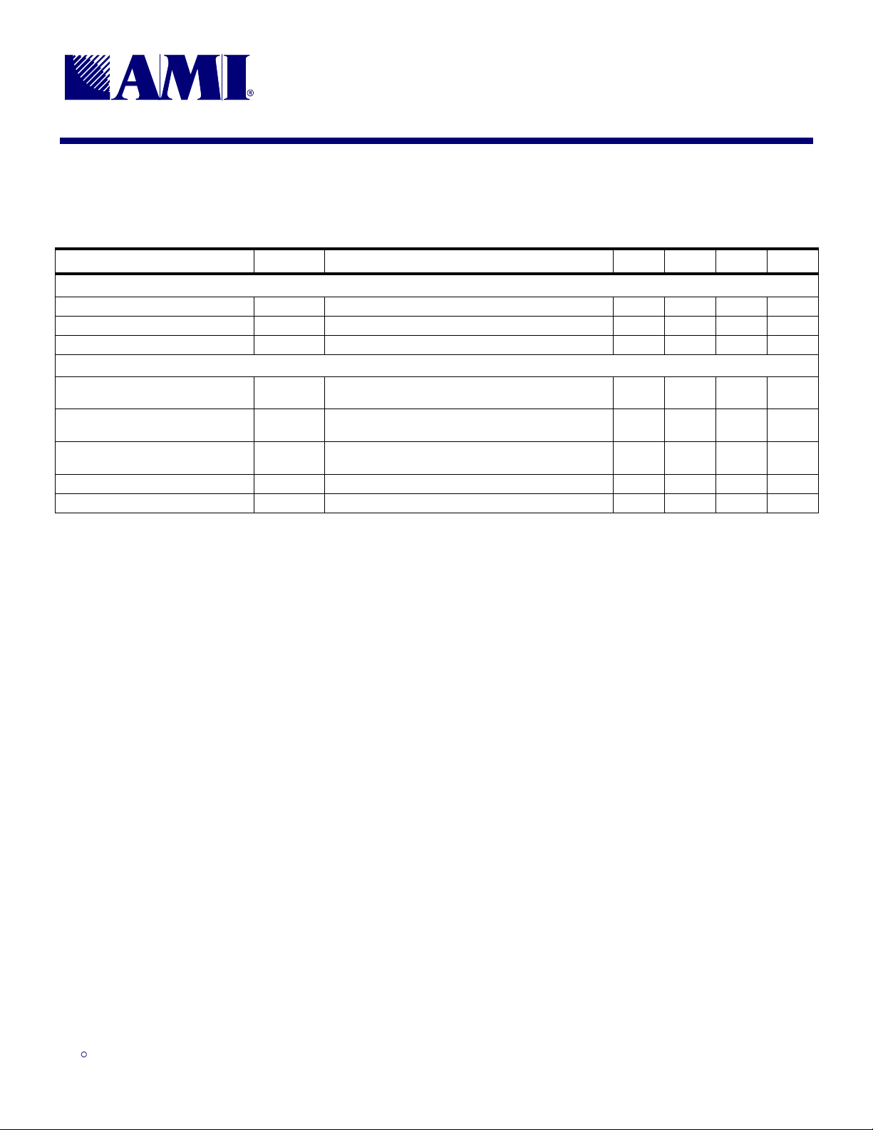
Table 6: AC Timing Specifications
Unless otherwise stated, VDD = 3.3V ± 10%, no load on any output, and ambient temperature range TA = 0°C to 70°C. Parameters denoted with an asterisk ( * ) represent nominal characterization
data and are not production tested to any specific limits. Where given, MIN and MAX characterization data are ± 3σ from typical.
PARAMETER SYMBOL CONDITIONS/DESCRIPTION MIN. TYP. MAX. UNITS
Overall
VCXO Stabilization Time * t
PLL Stabilization Time * t
Synthesis Error (unless otherwise noted in Frequency Table) 0 ppm
Clock Output (CLK)
Duty Cycle *
Jitter, Period (peak-peak) *
Jitter, Long Term (σy(τ)) *
Rise Time * t
Fall Time * t
VCXOSTB
PLLSTB
t
j(∆P)
t
j(LT)
r
f
From power valid 10 ms
From VCXO stable 100 us
Ratio of high pulse width (as measured from rising
edge to next falling edge at V
From rising edge to next rising edge at VDD/2, CL =
10pF
From 0-500µs at VDD/2, CL = 10pF
compared to ideal clock source
VDD = 3.3V; VO = 0.3V to 3.0V; CL = 10pF 1.7 ns
VDD = 3.3V; VO = 3.0V to 0.3V; CL = 10pF 1.7 ns
/2) to one clock period
DD
45 55 %
200 ps
100 ps
ISO9001
ISO9001
ISO9001ISO9001
5
4.24.00
Page 6
FS6128-04 / FS6128-05 / FS6128-06
FS6128-04 / FS6128-05 / FS6128-06
FS6128-04 / FS6128-05 / FS6128-06FS6128-04 / FS6128-05 / FS6128-06
PLL Clock Generator IC with VCXO
PLL Clock Generator IC with VCXO
PLL Clock Generator IC with VCXOPLL Clock Generator IC with VCXO
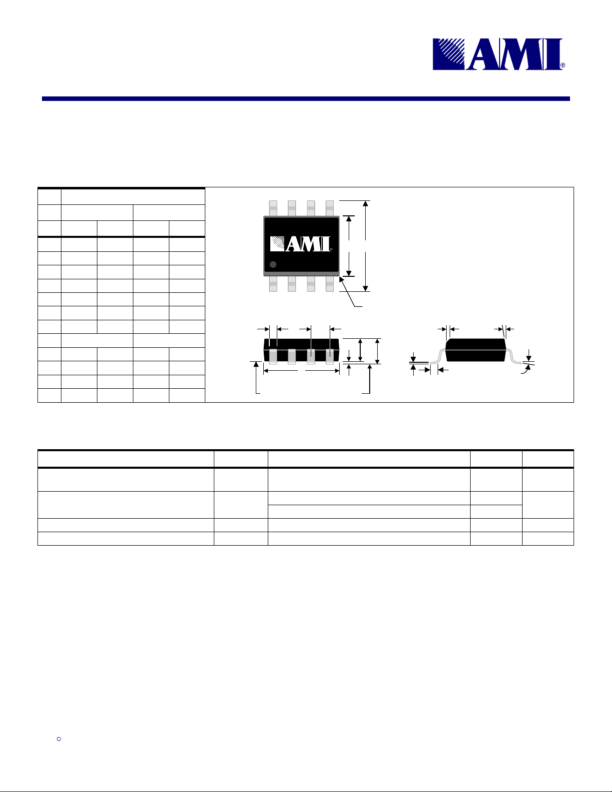
5.0 Package Information
Table 7: 8-pin SOIC (0.150") Package Dimensions
DIMENSIONS
INCHES MILLIMETERS
MIN. MAX. MIN. MAX.
A 0.061 0.068 1.55 1.73
A1 0.004 0.0098 0.102 0.249
A2 0.055 0.061 1.40 1.55
B 0.013 0.019 0.33 0.49
C 0.0075 0.0098 0.191 0.249
D 0.189 0.196 4.80 4.98
E 0.150 0.157 3.81 3.99
e 0.050 BSC 1.27 BSC
H 0.230 0.244 5.84 6.20
h 0.010 0.016 0.25 0.41
L 0.016 0.035 0.41 0.89
Θ 0° 8° 0° 8°
8
AMERICAN MICROSYSTEMS, INC.
1
B
D
BASE
PLANE
e
R
A
SEATING
PLANE
HE
ALL RADII:
0.005" TO 0.01"
A
A
2
1
AMERICAN MICROSYSTEMS, INC.
7° typ.h x 45°
C
L
April 2000
θ
Table 8: 8-pin SOIC (0.150") Package Characteristics
PARAMETER SYMBOL CONDITIONS/DESCRIPTION TYP. UNITS
Thermal Impedance, Junction to Free-Air
8-pin 0.150” SOIC
Lead Inductance, Self L
Lead Inductance, Mutual L
Lead Capacitance, Bulk C
Θ
JA
11
12
11
Air flow = 0 m/s 110 °C/W
Corner lead 2.0
Center lead 1.6
Any lead to any adjacent lead 0.4 nH
Any lead to V
SS
nH
0.27 pF
ISO9001
ISO9001
ISO9001ISO9001
6
4.24.00
Page 7
FS6128-04 / FS6128-05 / FS6128-06
FS6128-04 / FS6128-05 / FS6128-06
FS6128-04 / FS6128-05 / FS6128-06FS6128-04 / FS6128-05 / FS6128-06
AMERICAN MICROSYSTEMS, INC.
April 2000
6.0 Ordering Information
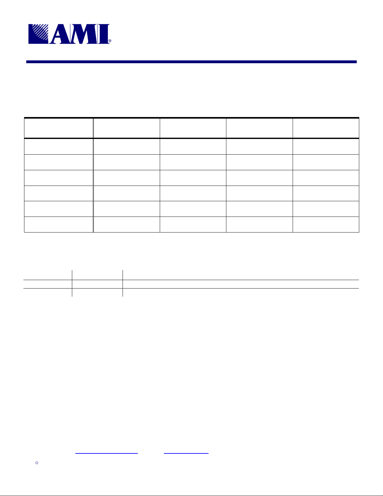
Table 9: Device Ordering Codes
ORDERING CODE DEVICE NUMBER PACKAGE TYPE
11640-825
11640-835
11640-102
11640-112
11640-103
11640-113
FS6128-04
FS6128-04
FS6128-05
FS6128-05
FS6128-06
FS6128-06
8-pin (0.150”) SOIC
(Small Outline Package)
8-pin (0.150”) SOIC
(Small Outline Package)
8-pin (0.150”) SOIC
(Small Outline Package)
8-pin (0.150”) SOIC
(Small Outline Package)
8-pin (0.150”) SOIC
(Small Outline Package)
8-pin (0.150”) SOIC
(Small Outline Package)
PLL Clock Generator IC with VCXO
PLL Clock Generator IC with VCXO
PLL Clock Generator IC with VCXOPLL Clock Generator IC with VCXO
OPERATING
TEMPERATURE RANGE
0°C to 70°C (Commer cial)
0°C to 70°C (Commer cial)
0°C to 70°C (Commer cial)
0°C to 70°C (Commer cial)
0°C to 70°C (Commer cial)
0°C to 70°C (Commer cial)
SHIPPING
CONFIGURATION
Tape and Reel
Tubes
Tape and Reel
Tubes
Tape and Reel
Tubes
7.0 Revision Information
DATE PAGE DESCRIPTION
1/21/00 1 Fixed typographical error
4/24/00 5 Fixed formatting error
Copyright © 2000 American Microsystems, Inc.
Devices sold by AMI are covered by the warranty and patent indemnification provisions appearing in its Terms of Sale only. AMI
makes no warranty, express, statutory implied or by description, regarding the information set forth herein or regarding the freedom
of the described devices from patent infringement. AMI makes no warranty of merchantability or fitness for any purposes. AMI reserves the right to discontinue production and change specifications and prices at any time and without notice. AMI’s products are
intended for use in commercial applications. Applications requiring extended temperature range, unusual environmental requirements, or high reliability applications, such as military, medical life-support or life-sustaining equipment, are specifically not recommended without additional processing by AMI for such applications.
American Microsystems, Inc., 2300 Buckskin Rd., Pocatello, ID 83201, (208) 233-4690, FAX (208) 234-6796,
WWW Address: http://www.amis.com E-mail: [email protected]
ISO9001
ISO9001
ISO9001ISO9001
7
4.24.00
 Loading...