

Page 1
On-State Current
4 Amp
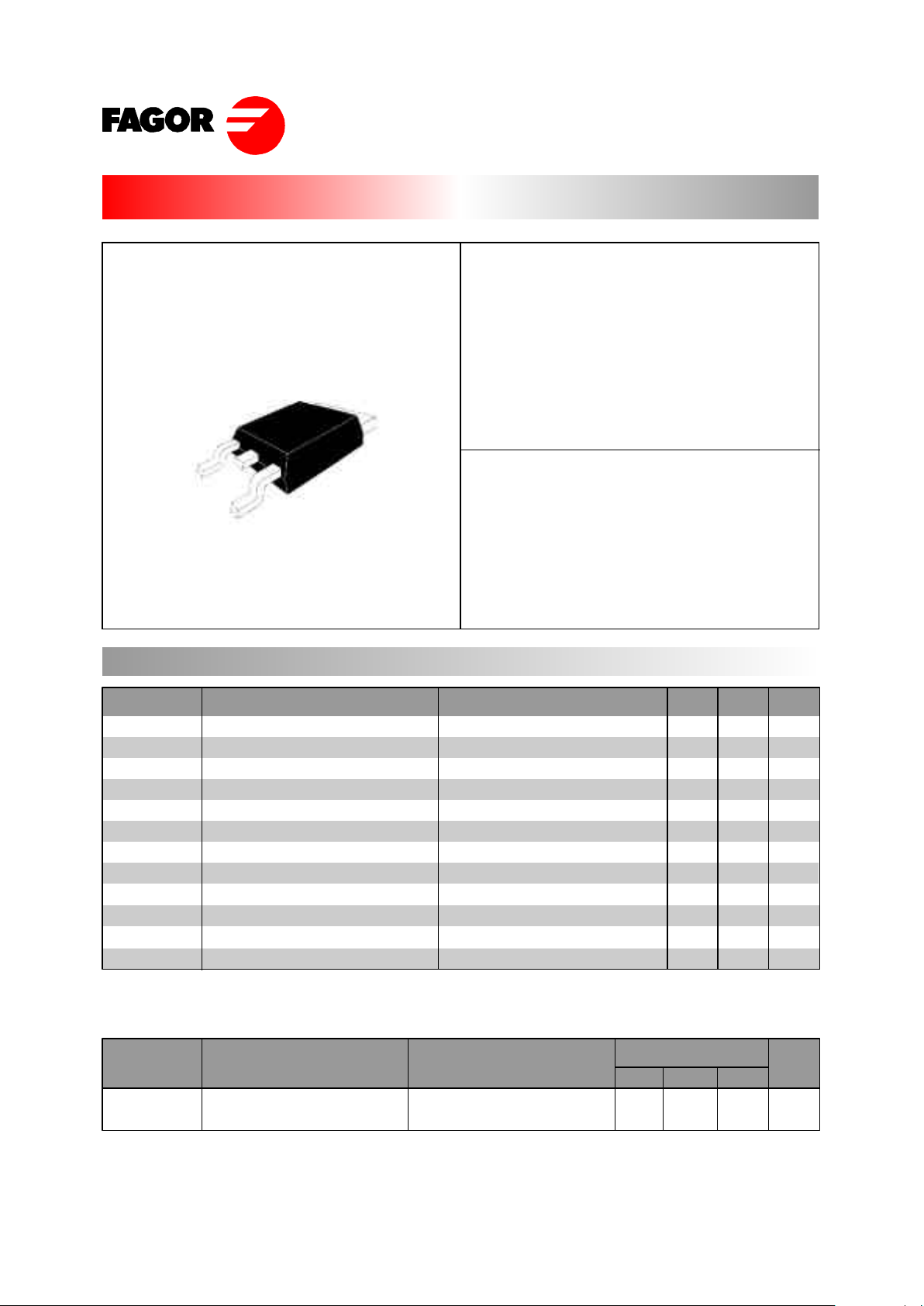
FS04...D
SURFACE MOUNT SCR
These series of Silicon Controlled
Rectifier use a high performance
PNPN technology.
These par ts are intended for general
purpose applications where high gate
sensitivity is required using surface
mount technology.
Jun - 02
Absolute Maximum Ratings, according to IEC publication No. 134
On-state Current
Average On-State Current
Non-repetitive On-State Current
Non-repetitive On-State Current
Fusing Current
Peak Reverse Gate Voltage
Peak Gate Current
Peak Gate Dissipation
Gate Dissipation
Operating Temperature
Storage Temperature
Soldering Temperature
I
T(RMS)
PARAMETER CONDITIONS Min. Max. Unit
DPAK
(Plastic)
Gate Trigger Current
< 200 µA
Off-State Voltage
200 V ÷ 600 V
SYMBOL
I
T(AV)
I
TSM
I2t
V
GRM
I
GM
P
G(AV)
T
j
T
stg
T
sld
180º Conduction Angle, TC = 115 ºC
Half Cycle, Θ=180º, T
C
= 115 ºC
Half Cycle, 60 Hz
Half Cycle, 50 Hz
t = 10 ms, Half Cycle
I
GR
= 10µA
20 µs max.
20 µs max.
20 ms max.
10s max
4
2.5
33
30
4.5
8
-40
-40
A
A
A
A
A
2
s
V
A
W
W
ºC
ºC
ºC
1.2
3
0.2
+125
+150
260
Repetitive Peak Off State
Voltage
PARAMETER CONDITIONS VOLTAGE UnitSYMBOL
V
DRM
V
RRM
R
GK
= 1 KΩ
B
200 V
D
400
I
TSM
P
GM
K
A
G
A
M
600
Page 2
FS04...D
SURFACE MOUNT SCR
Jun - 02
Electrical Characteristics
Gate Trigger Current
Off-State Leakage Current
On-state Voltage
Gate Trigger Voltage
Gate Non Trigger Voltage
Holding Current
Latching Current
PARAMETER CONDITIONS SENSITIVITY
Unit
SYMBOL
I
GT
I
DRM
VD = 12 V
DC
, R
L
= 33Ω. T
j
= 25 ºC
01
1
20
µA
04
15
5002200
03
20
200
1
5
1.6
0.8
0.1
5
6
10 10 5 10
mA
µA
V
V
V
mA
mA
V/µs
MIN
MAX
MAX
MAX
MAX
MAX
MIN
MAX
MAX
MIN
MIN
50
3
70
A/µs
/ I
RRM
V
TM
V
GT
I
H
I
L
dv / dt
di / dt
R
th(j-c)
R
th(j-a)
Critical Rate of Voltage
Rise
Critical Rate of Current Rise
Thermal Resistance
Junction-Case for DC
Thermal Resistance
Junction-Amb (S=0.5 cm
2
)
ºC/W
ºC/W
V
D
= V
DRM
, R
GK
= 220Ω, T
j
= 125 ºC
T
j
= 25 ºC
V
R
= V
RRM
,
at IT = 8 Amp, tp = 380 µs, Tj = 25 ºC
VD = 12 V
DC
, R
L
= 33Ω, T
j
= 25 ºC
I
T
= 50 mA , R
GK
= 1KΩ, T
j
= 25 ºC
I
G
= 1 mA , R
GK
= 1KΩ, T
j
= 25 ºC
V
D
= 0.67 x V
DRM
, R
GK
= 220Ω,
T
j
= 125 ºC
PART NUMBER INFORMATION
V
GD
VD =V
DRM
, R
L
= 3.3 KΩ, RGK = 220Ω
T
j
= 125 ºC
FAGOR
SCR
CURRENT
CASE
VOLTAGE
SENSITIVITY
F S 04 01 B D 00
FORMING
TR
PACKAGING
Tr ≤ 100 ns, F = 60 Hz,
T
j
= 125 ºC
I
G
= 2 x I
GT
Page 3

2.0
1.8
1.6
1.4
1.2
1.0
0.8
0.6
0.4
0.2
0
Igt (Tj)
Fig. 5: Relative variation of gate trigger current
and holding current versus junction temperature.
-40 -20 0 60 80 100 120 140
Igt (Tj = 25 ºC)
Ih (Tj)
Ih (Tj = 25 ºC)
4020
Tj (ºC)
Ih
Igt
1.00
0.10
0.01
K=[Zth(j-a) / Rth(j-a)]
Fig. 4-2: Relative variation of thermal
impedance junction to ambient versus pulse
duration. (recommended pad layout)
1E-2 1E-1 1E+0 1E+1 1E+2 5E+2
tp (s)
Tamb (ºC)
FS04...D
SURFACE MOUNT SCR
0
4.0
3.5
3.0
2.5
2.0
1.5
1.0
0.5
0
0.5 1 1.5
P (W)
Fig. 1: Maximum average power dissipation
versus average on-state current
0
4.0
3.5
3.0
2.5
2.0
1.5
1.0
0.5
0
25 50 100 125
P (W)
Fig. 2: Correlation between maximum average power dissipation and
maximum allowable temperatures (Tamb and T case) for different
thermal resistances heatsink+contact.
T case (ºC)
125
Fig. 3: Average and DC on-state current versus
ambient temperature (device mounted on FR4
with recommended pad layout)
Jun- 02
2.0
1.8
1.6
1.4
1.2
1.0
0.8
0.6
0.4
0.2
0
I
T(AV)
(A)
0 25 100 12550 75
2 2.5 3
Tamb (ºC)
I
T(AV)
(A)
3.5
α
360 º
75
120
115
Rth= 37C/W
Rth= 15C/W
Rth= 10C/W
Rth= 0C/W
Rth= 5C/W
α=180º
α = 180 º
DC
1.0
0.5
0.2
0.1
K=[Zth(j-c) / Rth(j-c)]
Fig. 4-1: Relative variation of thermal
impedance junction to case versus pulse
duration.
1E-3 1E-2 1E-1 1E+0
tp (s)
α = 80 º
Page 4

S(cm)
Fig. 9: Thermal resistance junction to ambient versus
copper surface under tab (Epoxy printed circuit
board FR4, copper thickness: 35µm).
100
80
60
40
20
0
I
th(j-a)
(ºC/W)
0 2 8 104 6 12 14 16 18 20
t(s)
Fig. 10: Typical reflow soldering heat profile, either
for mounting on FR4 or metal-backed boards.
250
200
150
100
50
0
T(ºC)
0 40 160 20080 120 240 280 320 360
215ºC
245ºC
Epoxy FR4
board
Metal-backed
board
1 10 100 1000
Fig. 6: Non repetitive surge peak on-state
current versus number of cycles.
35
30
25
20
15
10
5
0
I
TSM
(A)
Number of cycles
Tj initial = 25 ºC
F= 50Hz
Jun - 02
FS04...D
SURFACE MOUNT SCR
tp(ms)
I
TSM
(A). I2t (A2s)
Fig. 7: Non repetitive surge peak on-state
current for a sinusoidal pulse with width:
tp <10 ms, and corresponding value of I
2
t.
100
10
1
1 10
Tj initial = 25 ºC
I
TSM
2 5
Fig. 8: On-state characteristics (maximum
values).
50.0
10.0
ITM(A)
0 0.5 1 1.5 2 2.5 3 3.5 4
VTM(V)
1.0
0.1
Tj max
Vto = 0.85 V
Rd =90mΩ
Tj=Tj max
Tj25 ºC
I
2
t
Page 5

Jun - 02
FS04...D
SURFACE MOUNT SCR
PACKAGE MECHANICAL DATA
DPAK TO 252-AA
A
A1
b
c
c1
c2
D
D1
E
E1
e
H
L
L1
L2
L3
L4
REF.
DIMENSIONS
Milimeters
Min. Nominal Max.
2.18
0
0.64
0.46
0.46
5.97
5.21
6.35
5.20
9.40
1.40
2.55
0.46
0.89
0.64
2.3±0.18
0.12
0.75±0.1
0.8±0.013
6.1±0.1
6.58±0.14
5.36±0.1
2.28BSC
9.90±0.15
2.6±0.05
0.5±0.013
1.20±0.05
0.83±0.1
2.39
0.127
0.89
0.61
0.56
6.22
5.52
6.73
5.46
10.41
1.78
2.74
0.58
1.27
1.02
Marking: type number
Weight: 0.2 g
8º
±2º
E
L3
D
be
4.57 Typ.
ø1x0.15
H
1.6
L4
A
c2
8º
±2º
8º
±2º
8º
±2º
8º
±2º
L
L2
A1
1.067
±0.013
E1
D1
FOOT PRINT
6.7
6.7
3
1.6
2.32.3
1.6
3
 Loading...