

Page 1
On-State Current
4 Amp
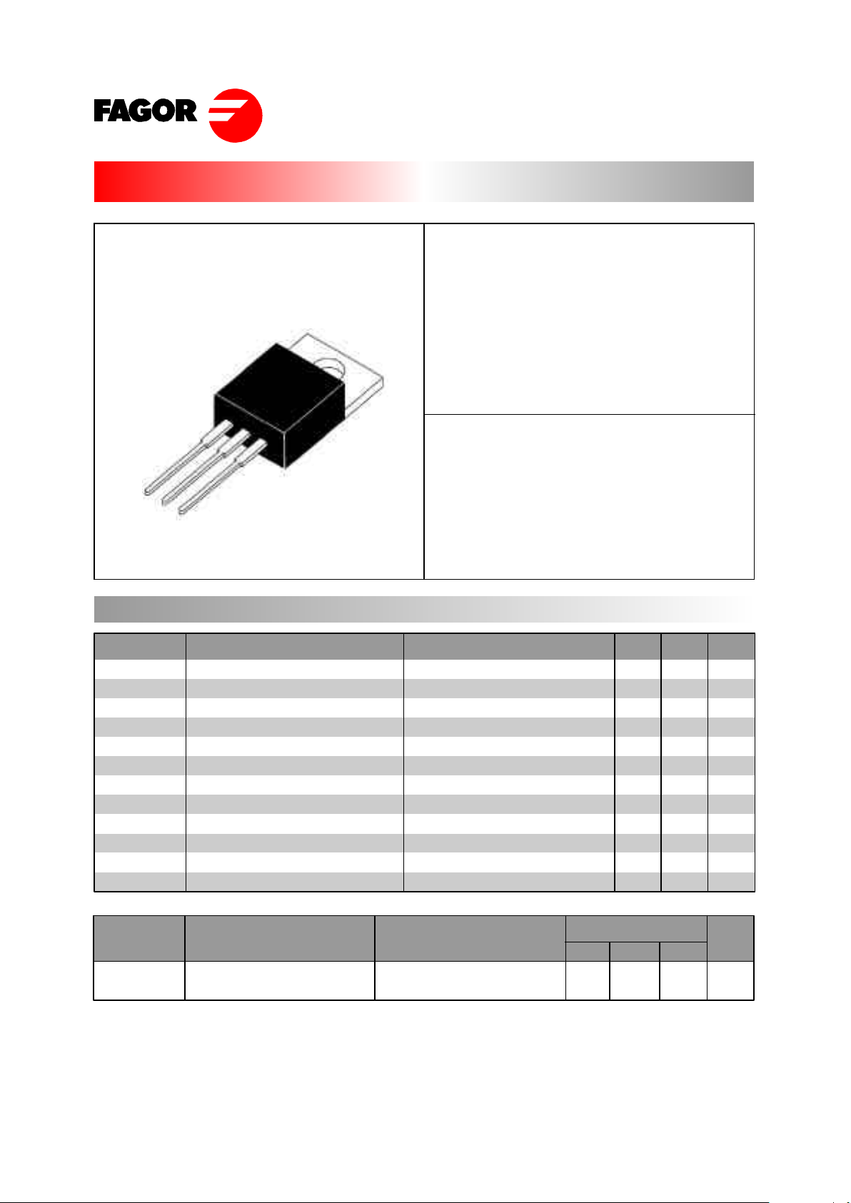
FS0402.H
SENSITIVE GATE SCR
These series of Silicon Controlled
R ectifier use a high performance
PNPN technology.
These parts are intended for general
purpose applications where high gate
sensitivity is required.
Feb - 03
Absolute Maximum Ratings, according to IEC publication No. 134
On-state Current
Average On-state Current
Non-repetitive On-State Current
Non-repetitive On-State Current
Fusing Current
Peak Reverse Gate Voltage
Peak Gate Current
Peak Gate Dissipation
Gate Dissipation
Operating Temperature
Storage Temperature
Soldering Temperature
I
T(RMS)
PARAMETER CONDITIONS Min. Max. Unit
Gate Trigger Current
< 200 µA
Off-State Voltage
200 V ÷ 600 V
SYMBOL
I
T(AV)
I
TSM
I
TSM
I2t
V
GRM
I
GM
P
GM
P
G(AV)
T
j
T
stg
T
sld
180º Conduction Angle, Tc = 115 ºC
Half Cycle, Θ = 180 º, T
C
= 115 ºC
Half Cycle, 60 Hz
Half Cycle, 50 Hz
t
p
= 10ms, Half Cycle
I
GR
= 10 µA
20 µs max.
20 µs max.
20ms max.
10s max.
-40
-40
A
A
A
A
A
2
s
V
A
W
W
ºC
ºC
ºC
4
2.5
33
30
4.5
8
4
5
0.5
+125
+150
260
Repetitive Peak Off State
Voltage
PARAMETER CONDITIONS VOLTAGE UnitSYMBOL
V
DRM
V
RRM
R
GK
= 1 KΩ
B
200 V
D
400
M
600
TO220-AB
K
A
G
A
Page 2

FS0402.H
SENSITIVE GATE SCR
Feb - 03
PART NUMBER INFORMATION
FAGOR
SCR
CURRENT
CASE
VOLTAGE
SENSITIVITY
F S 04 02 B H 00
FORMING
TU
PACKAGING
Electrical Characteristics
Gate Trigger Current
Off-State Leakage Current
On-state Voltage
Gate Trigger Voltage
Gate Non Trigger Voltage
Holding Current
PARAMETER CONDITIONS SENSITIVITY
Unit
SYMBOL
I
GT
I
DRM
VD = 12 V
DC
, R
L
= 33Ω. T
j
= 25 ºC
02
200
1
5
1.6
0.8
0.1
mA
µA
V
V
V
MAX
MAX
MAX
MAX
MIN
50
60
MAX
/ I
RRM
V
TM
V
GT
V
GD
I
H
di / dt
R
th(j-a)
Critical Rate of Current Rise
Thermal Resistance
Junction-Amb for DC
ºC/W
V
D
= V
DRM
, Tj = 125 ºC
T
j
= 25 ºC
V
R
= V
RRM
,
at IT = 8 Amp, tp = 380 µs, Tj = 25 ºC
IT = 50 mA,
Tr ≤ 100 ns, f = 60 Hz,
T
j
= 125 ºC
VD = 12 V
DC
, R
L
= 33Ω, T
j
= 25 ºC
V
D
= V
DRM
, R
L
= 3.3KΩ,
T
j
= 125 ºC
mA
MIN
A/µs
R
d
T
j
= 125 ºC
R
d
Dynamic resistance MAX
90
mΩ
5
MAX
I
L
mA
6
Latching Current
I
G
= 1 mA,
V/µs
dv / dt
Critical Rate of Voltage Rise MIN
5
3
R
th(j-c)
Thermal Resistance
Junction-Case for DC
ºC/W
V
t0
T
j
= 125 ºC
Threshold Voltage MAX
0.85
V
IG = 2 x I
GT
R
GK
= 220Ω
R
GK
= 220Ω
R
GK
= 220Ω
T
j
= 25 ºC
R
GK
= 1 KΩ
V
D
= 0.65 x V
DRM
, R
GK
= 220Ω,
T
j
= 125 ºC
µA
MAX
Page 3

Feb - 03
Fig. 1: Maximum average power dissipation
versus average on-state current.
FS0402.H
SENSITIVE GATE SCR
0 2
5
4
3
2
1
0
P (W)
I
T(av)
(A)
0.5 3
α
360 º
Fig. 2: Average and D.C. on-state current
versus case temperature.
I
T(av)
(A)
T case (ºC)
5
4
3
2
1
0
0 25 50 75 100 125
α = 180 º
D.C.
1 1.5 2.5 3.5
1.0
[Zth(j-c) / Rth (j-c)]
1E-3 1E-2 1E-1 1E+0
tp (s)
0.5
0.2
0.1
IGT, IH (Tj) / IGT, IH (Tj = 25 ºC)
Tj (ºC)
2.0
1.8
1.6
1.4
1.2
1.0
0.8
0.6
0.4
0.2
0.0
-40 -20 20 60 80 1000 40 120 140
IGT
IH & IL
Fig. 5: Non repetitive surge peak on-state
current versus number of cycles.
Fig. 6: Non repetitive surge peak on-state
current for a sinusoidal pulse with width:
tp < 10 ms, and corresponding value of I
2
t.
Fig. 3: Relative variation of thermal impedance
junction to case versus pulse duration.
Fig. 4: Relative variation of gate trigger
current, holding and latching current versus
junction temperature.
1 10 100 1000
35
30
25
20
15
10
5
0
I
TSM
(A)
Number of cycles
Tj initial = 25 ºC
F= 50Hz
tp(ms)
I
TSM
(A). I2t (A2s)
100
10
1
1 10
Tj initial = 25 ºC
I t
I
TSM
2 5
Page 4

Feb - 03
FS0402.H
SENSITIVE GATE SCR
Fig. 7: On-state characteristics (maximum
values).
50.0
10.0
ITM(A)
0 0.5 1 1.5 2 2.5 3 3.5 4
VTM(V)
1.0
0.1
Tj max
Vto = 0.85 V
Rd =90mΩ
Tj=Tj max
Tj25 ºC
PACKAGE MECHANICAL DATA
TO-220AB
A
a1
a2
B
b1
b2
C
c1
c2
e
F
I
I4
L
I2
I3
M
REF.
DIMENSIONS
Milimeters
Min. Nominal Max.
15.20
13.00
10.00
0.61
1.23
4.40
0.49
2.40
2.40
6.20
3.75
15.80
2.65
1.14
1.14
3.75
16.40
2.60
15.90
14.00
10.40
0.88
1.32
4.60
0.70
2.72
2.70
6.60
3.85
16.80
2.95
1.70
1.70
14
a1
L
A
e
a2
b1
12
13
øI
B
c
F
b2
c2
c1
M
 Loading...