

Page 1
June 1998
FRS234D, FRS234R,
FRS234H
5A, 250V, 0.715 Ohm, Rad Hard,
N-Channel Power MOSFETs
Features
• 5A, 250V, RDS(on) = 0.715Ω
• Second Generation Rad Hard MOSFET Results From New Design Concepts
• Gamma - Meets Pre-Rad Specifications to 100KRAD(Si)
- Defined End Point Specs at 300KRAD(Si) and 1000KRAD(Si)
- Performance Permits Limited Use to 3000KRAD(Si)
• Gamma Dot - Survives 3E9RAD(Si)/sec at 80% BVDSS Typically
- Survives 2E12 Typically If Current Limited to IDM
• Photo Current - 4.0nA Per-RAD(Si)/sec Typically
• Neutron - Pre-RAD Specifications for 1E13 Neutrons/cm
- Usable to 1E14 Neutrons/cm
2
2
Description
The Intersil Corporation has designed a series of SECOND GENERATION hardened power MOSFETs of both N and P channel enhancement types with ratings
from 100V to 500V, 1A to 60A, and on resistance as low as 25mΩ. Total dose
hardness is offered at 100K RAD(Si) and 1000KRAD(Si) with neutron hardness
ranging from 1E13n/cm
rate hardness (GAMMA DOT) exists for rates to 1E9 without current limiting and
2E12 with current limiting.
This MOSFET is an enhancement-mode silicon-gate power field effect transistor of
the vertical DMOS (VDMOS) structure. It is specially designed and processed to
exhibit minimal characteristic changes to total dose (GAMMA) and neutron (n
exposures. Design and processing efforts are also directed to enhance survival to
heavy ion (SEE) and/or dose rate (GAMMA DOT) exposure.
2
for 500V product to 1E14n/cm2 for 100V product. Dose
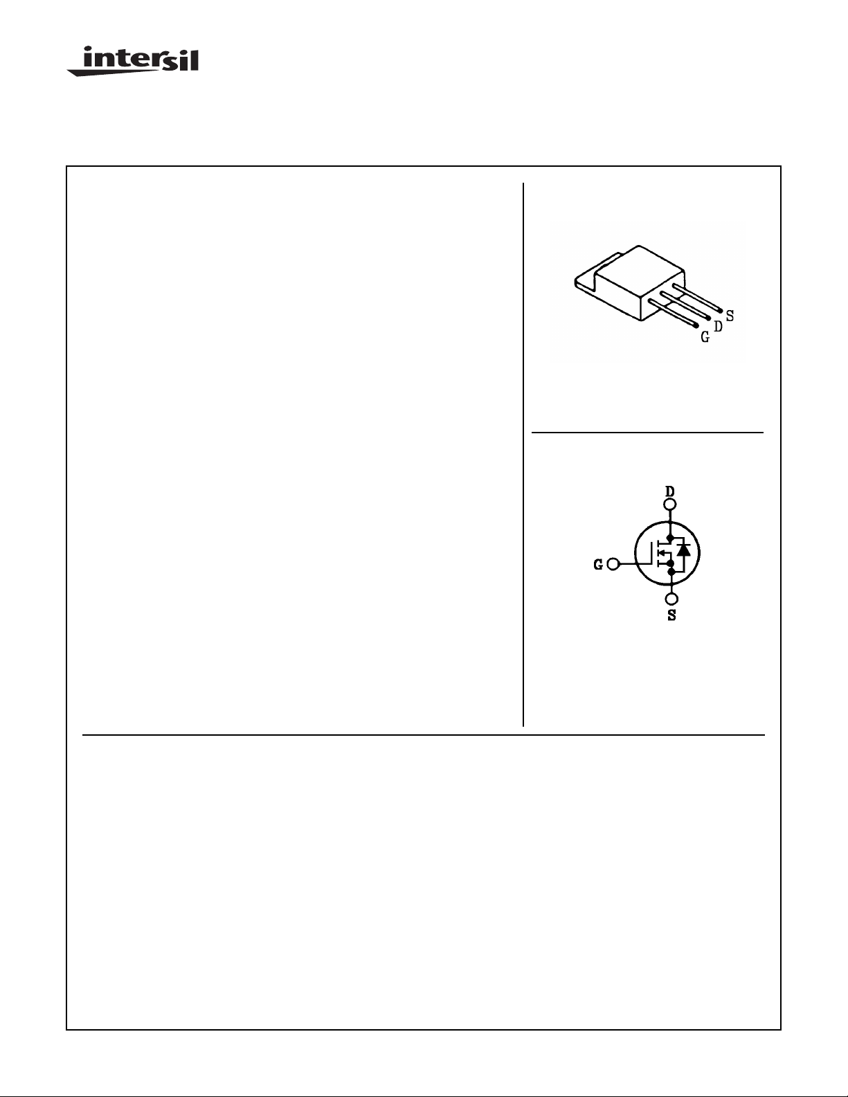
Package
TO-257AA
CAUTION: Beryllia Warning per MIL-S-19500
refer to package specifications.
Symbol
o
)
This part may be supplied as a die or in various packages other than shown above .
Reliability screening is available as either non TX (commercial), TX equivalent of
MIL-S-19500, TXV equivalent of MIL-S-19500, or space equivalent of
MIL-S-19500. Contact the Intersil High-Reliability Marketing group for any desired
deviations from the data sheet.
Absolute Maximum Ratings (TC = +25
Drain-Source Voltage. . . . . . . . . . . . . . . . . . . . . . . . . . . . . . . . . . . . . . . . . . . . . . . . . . . . . . .VDS 250 V
Drain-Gate Voltage (RGS = 20kΩ). . . . . . . . . . . . . . . . . . . . . . . . . . . . . . . . . . . . . . . . . . . VDGR 250 V
Continuous Drain Current
TC = +25
TC = +100oC . . . . . . . . . . . . . . . . . . . . . . . . . . . . . . . . . . . . . . . . . . . . . . . . . . . . . . . . . . . . .ID
Pulsed Drain Current. . . . . . . . . . . . . . . . . . . . . . . . . . . . . . . . . . . . . . . . . . . . . . . . . . . . . . . IDM 15 A
Gate-Source Voltage . . . . . . . . . . . . . . . . . . . . . . . . . . . . . . . . . . . . . . . . . . . . . . . . . . . . . . .VGS ±20 V
Maximum Power Dissipation
TC = +25oC . . . . . . . . . . . . . . . . . . . . . . . . . . . . . . . . . . . . . . . . . . . . . . . . . . . . . . . . . . . . . PT
TC = +100oC . . . . . . . . . . . . . . . . . . . . . . . . . . . . . . . . . . . . . . . . . . . . . . . . . . . . . . . . . . . . PT
Derated Above +25oC . . . . . . . . . . . . . . . . . . . . . . . . . . . . . . . . . . . . . . . . . . . . . . . . . . . . . . .
Inductive Current, Clamped, L = 100µH, (See Test Figure). . . . . . . . . . . . . . . . . . . . . . . . . . ILM 15 A
Continuous Source Current (Body Diode). . . . . . . . . . . . . . . . . . . . . . . . . . . . . . . . . . . . . . . . .IS 5 A
Pulsed Source Current (Body Diode) . . . . . . . . . . . . . . . . . . . . . . . . . . . . . . . . . . . . . . . . . . ISM 15 A
Operating And Storage Temperature. . . . . . . . . . . . . . . . . . . . . . . . . . . . . . . . . . . . . TJC, TSTG -55 to +150
Lead Temperature (During Soldering)
Distance > 0.063 in. (1.6mm) From Case, 10s Max. . . . . . . . . . . . . . . . . . . . . . . . . . . . . . . TL 300
o
C . . . . . . . . . . . . . . . . . . . . . . . . . . . . . . . . . . . . . . . . . . . . . . . . . . . . . . . . . . . . . .ID
o
C) Unless Otherwise Specified
FRS234D, R, H UNITS
5
3
50
20
0.40
A
A
W
W
W/oC
o
C
o
C
CAUTION: These devices are sensitive to electrostatic discharge; follow proper IC Handling Procedures.
http://www.intersil.com or 407-727-9207
| Copyright © Intersil Corporation 1999
4-1
File Number 3251.2
Page 2
FRS234D, FRS234R, FRS234H
Pre-Radiation Electrical Specifications TC = +25
o
C, Unless Otherwise Specified
LIMITS
PARAMETER SYMBOL TEST CONDITIONS
UNITSMIN MAX
Drain-Source Breakdown Volts BVDSS VGS = 0, ID = 1mA 250 - V
Gate-Threshold Volts VGS(th) VDS = VGS, ID = 1mA 2.0 4.0 V
Gate-Body Leakage Forward IGSSF VGS = +20V - 100 nA
Gate-Body Leakage Reverse IGSSR VGS = -20V - 100 nA
Zero-Gate Voltage
Drain Current
IDSS1
IDSS2
IDSS3
VDS = 250V, VGS = 0
VDS = 200V, VGS = 0
VDS = 200V, VGS = 0, TC = +125oC
-
-
-
1
0.025
0.25
mA
Rated Avalanche Current IAR Time = 20µs - 15 A
Drain-Source On-State Volts VDS(on) VGS = 10V, ID = 5A - 3.75 V
Drain-Source On Resistance RDS(on) VGS = 10V, ID = 3A - 0.715 Ω
Turn-On Delay Time td(on) VDD = 125V, ID = 5A - 34
Rise Time tr Pulse Width = 3µs-80
ns
Turn-Off Delay Time td(off) Period = 300µs, Rg = 25Ω - 180
Fall Time tf 0 ≤ VGS ≤ 10 (See Test Circuit) - 64
Gate-Charge Threshold QG(th)
0.5 3
ncGate-Charge On State QG(on) 16 68
Gate-Charge Total QGM 32 128
VDD = 125V, ID = 5A
IGS1 = IGS2
Plateau Voltage VGP 3 12 V
0 ≤ VGS ≤ 20
Gate-Charge Source QGS 2 8
nc
Gate-Charge Drain QGD 10 40
Diode Forward Voltage VSD ID = 5A, VGD = 0 0.6 1.8 V
Reverse Recovery Time TT I = 5A; di/dt = 100A/µs - 1200 ns
Junction-To-Case Rθjc - 2.5
o
C/W
Junction-To-Ambient Rθja Free Air Operation - 60
0V
VGS = 12V
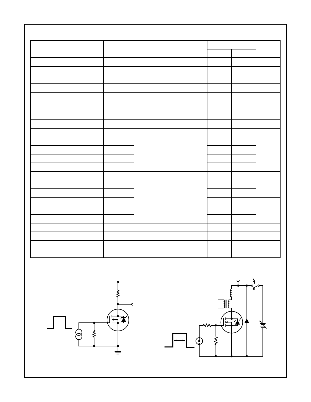
ELECTRONIC SWITCH OPENS
50Ω
L
WHEN I
V
DS
V
DD
R
L
V
DS
VARY t
TO OBTAIN
DUT
R
GS
0V
P
REQUIRED PEAK I
VGS≤ 20V
t
P
CURRENT
TRANSFORMER
AS
50Ω
+
I
AS
-
DUT
IS REACHED
AS
FIGURE 1. RESISTIVE SWITCHING TEST CIRCUIT FIGURE 2. UNCLAMPED ENERGY TEST CIRCUIT
4-2
+
V
DD
-
50V-150V
Page 3

FRS234D, FRS234R, FRS234H
Post-Radiation Electrical Specifications TC = +25
PARAMETER SYMBOL TYPE TEST CONDITIONS
Drain-Source
Breakdown Volts
Gate-Source
Threshold Volts
Gate-Body
Leakage Forward
Gate-Body
Leakage Reverse
Zero-Gate Voltage
Drain Current
Drain-Source
On-State Volts
(Note 4, 6) BVDSS FRS234D, R VGS = 0, ID = 1mA 250 - V
(Note 5, 6) BVDSS FRS234H VGS = 0, ID = 1mA 238 - V
(Note 4, 6) VGS(th) FRS234D, R VGS = VDS, ID = 1mA 2.0 4.0 V
(Note 3, 5, 6) VGS(th) FRS234H VGS = VDS, ID = 1mA 1.5 4.5 V
(Note 4, 6) IGSSF FRS234D, R VGS = 20V, VDS = 0 - 100 nA
(Note 5, 6) IGSSF FRS234H VGS = 20V, VDS = 0 - 200 nA
(Note 2, 4, 6) IGSSR FRS234D, R VGS = -20V, VDS = 0 - 100 nA
(Note 2, 5, 6) IGSSR FRS234H VGS = -20V, VDS = 0 - 200 nA
(Note 4, 6) IDSS FRS234D, R VGS = 0, VDS = 200V - 25 µA
(Note 5, 6) IDSS FRS234H VGS = 0, VDS = 200V - 100 µA
(Note 1, 4, 6) VDS(on) FRS234D, R VGS = 10V, ID = 5A - 3.75 V
(Note 1, 5, 6) VDS(on) FRS234H VGS = 16V, ID = 5A - 5.63 V
o
C, Unless Otherwise Specified
LIMITS
UNITSMIN MAX
Drain-Source
On Resistance
NOTES:
1. Pulse test, 300µs max
2. Absolute value
3. Gamma = 300KRAD(Si)
4. Gamma = 10KRAD(Si) for “D”, 100KRAD(Si) for “R”. Neutron = 1E13
5. Gamma = 1000KRAD(Si). Neutron = 1E13
6. Insitu Gamma bias must be sampled for both VGS = +10V, VDS = 0V and VGS = 0V, VDS = 80% BVDSS
7. Gamma data taken 1/19/90 on TA 17633 devices by GE ASTRO SPACE; EMC/SURVIVABILITY LABORATORY; KING OF PRUSSIA,
PA 19401
8. Single event drain burnout testing by Titus, J.L., et al of NWSC, Crane, IN at Brookhaven Nat. Lab. Dec 11-14, 1989
9. Neutron derivation, Intersil Application note AN-8831, Oct. 1988
(Note 1, 4, 6) RDS(on) FRS234D, R VGS = 10V, ID = 3A - 0.715 Ω
(Note 1, 5, 6) RDS(on) FRS234H VGS = 14V, ID = 3A - 1.073 Ω
4-3
Page 4

FRS234D, FRS234R, FRS234H
Typical Performance Characteristics
4-4
Page 5

FRS234D, FRS234R, FRS234H
Rad Hard Data Packages - Intersil Power Transistors
TXV Equivalent
1. Rad Hard TXV Equivalent - Standard Data Package
A. Certificate of Compliance
B. Assembly Flow Chart
C. Preconditioning - Attributes Data Sheet
D. Group A - Attributes Data Sheet
E. Group B - Attributes Data Sheet
F. Group C - Attributes Data Sheet
G. Group D - Attributes Data Sheet
2. Rad Hard TXV Equivalent - Optional Data Package
A. Certificate of Compliance
B. Assembly Flow Chart
C. Preconditioning - Attributes Data Sheet
- Precondition Lot Traveler
- Pre and Post Burn-In Read and Record
Data
D. Group A - Attributes Data Sheet
- Group A Lot Traveler
E. Group B - Attributes Data Sheet
- Group B Lot Traveler
- Pre and Post Read and Record Data for
Intermittent Operating Life (Subgroup B3)
- Bond Strength Data (Subgroup B3)
- Pre and Post High Temperature Operating
Life Read and Record Data (Subgroup B6)
F. Group C - Attributes Data Sheet
- Group C Lot Traveler
- Pre and Post Read and Record Data for
Intermittent Operating Life (Subgroup C6)
- Bond Strength Data (Subgroup C6)
G. Group D - Attributes Data Sheet
- Group D Lot Traveler
- Pre and Post RAD Read and Record Data
Class S - Equivalents
1. Rad Hard “S” Equivalent - Standard Data Package
A. Certificate of Compliance
B. Serialization Records
C. Assembly Flow Chart
D. SEM Photos and Report
E. Preconditioning Attributes Data Sheet
Hi-Rel Lot Traveler
HTRB - Hi Temp Gate Stress Post Reverse
Bias Data and Delta Data
HTRB - Hi T emp Drain Stress Post Reverse
Bias Delta Data
F. Group A - Attributes Data Sheet
G. Group B - Attributes Data Sheet
H. Group C - Attributes Data Sheet
I. Group D - Attributes Data Sheet
2. Rad Hard Max. “S” Equivalent - Optional Data Package
A. Certificate of Compliance
B. Serialization Records
C. Assembly Flow Chart
D. SEM Photos and Report
E. Preconditioning - Attributes Data Sheet
- Hi-Rel Lot Traveler
- HTRB - Hi Temp Gate Stress Post
Reverse Bias Data and Delta Data
- HTRB - Hi Temp Drain Stress Post
Reverse Bias Delta Data
- X-Ray and X-Ray Report
F. Group A - Attributes Data Sheet
- Hi-Rel Lot Traveler
- Subgroups A2, A3, A4, A5 and A7 Data
G. Group B - Attributes Data Sheet
- Hi-Rel Lot Traveler
- Subgroups B1, B3, B4, B5 and B6 Data
H. Group C - Attributes Data Sheet
- Hi-Rel Lot Traveler
- Subgroups C1, C2, C3 and C6 Data
I. Group D - Attributes Data Sheet
- Hi-Rel Lot Traveler
- Pre and Post Radiation Data
4-5
Page 6

FRS234D, FRS234R, FRS234H
TO-257AA
3 LEAD JEDEC TO-257AA HERMETIC METAL PACKAGE
E
Q
ØP
H
1
A
A
1
SYMBOL
A 0.190 0.200 4.83 5.08 -
A
1
INCHES MILLIMETERS
NOTESMIN MAX MIN MAX
0.035 0.045 0.89 1.14 -
Øb 0.025 0.035 0.64 0.88 2, 3
D
Øb
0.060 0.090 1.53 2.28 -
1
D 0.645 0.665 16.39 16.89 E 0.410 0.420 10.42 10.66 e 0.100 TYP 2.54 TYP 4
L
1
L
0.065 R TYP.
Øb
1
b
123
e
e
1
J
1
e
1
H
1
J
1
L 0.600 0.650 15.24 16.51 -
L
1
ØP 0.140 0.150 3.56 3.81 -
Q 0.113 0.133 2.88 3.37 -
NOTES:
0.200 BSC 5.08 BSC 4
0.230 0.250 5.85 6.35 -
0.110 0.130 2.80 3.30 4
- 0.035 - 0.88 -
1. These dimensions are within allowable dimensions of Re v. B of
JEDEC TO-257AA dated 9-88.
2. Add typically 0.002 inches (0.05mm) for solder coating.
3. Lead dimension (without solder).
4. Position of lead to be measured 0.150 inches (3.81mm) from bottom
of dimension D.
5. Die to base BeO isolated, terminals to case ceramic isolated.
6. Controlling dimension: Inch.
7. Revision 1 dated 1-93.
WARNING!
BERYLLIA WARNING PER MIL-S-19500
Packages containing beryllium oxide (BeO) shall not be ground, machined, sandblasted, or subject to any mechanical
operation which will produce dust containing any beryllium compound. Packages containing any beryllium compound
shall not be subjected to any chemical process (etching, etc.) which will produce fumes containing beryllium or its’
compounds.
All Intersil semiconductor products are manufactured, assembled and tested under ISO9000 quality systems certification.
Intersil products are sold by description only. Intersil Corporation reserves the right to make changes in circuit design and/or specifications at any time without
notice. Accordingly, the reader is cautioned to verify that data sheets are current before placing orders. Information furnished by Intersil is believed to be accurate
and reliable. However, no responsibility is assumed by Intersil or its subsidiaries for its use; nor for any infringements of patents or other rights of third parties which
may result from its use. No license is granted by implication or otherwise under an y patent or patent rights of Intersil or its subsidiaries.
For information regarding Intersil Corporation and its products, see web site http://www.intersil.com
Sales Office Headquarters
NORTH AMERICA
Intersil Corporation
P. O. Box 883, Mail Stop 53-204
Melbourne, FL 32902
TEL: (407) 724-7000
FAX: (407) 724-7240
EUROPE
Intersil SA
Mercure Center
100, Rue de la Fusee
1130 Brussels, Belgium
TEL: (32) 2.724.2111
FAX: (32) 2.724.22.05
ASIA
Intersil (Taiwan) Ltd.
Taiwan Limited
7F-6, No. 101 Fu Hsing North Road
Taipei, Taiwan
Republic of China
TEL: (886) 2 2716 9310
FAX: (886) 2 2715 3029
4-6
 Loading...