

Page 1
Any and all SANYO products described or contained herein do not have specifications that can handle
applications that require extremely high levels of reliability, such as life-support systems, aircraft’s
control systems, or other applications whose failure can be reasonably expected to result in serious
physical and/or material damage. Consult with your SANYO representative nearest you before using
any SANYO products described or contained herein in such applications.
SANYO assumes no responsibility for equipment failures that result from using products at values that
exceed, even momentarily, rated values (such as maximum ratings, operating condition ranges,or other
parameters) listed in products specifications of any and all SANYO products described or contained
herein.
PNP/NPN Epitaxial Planar Silicon Transistors
Push-Pull Circuit Applications
Ordering number:ENN6457
FP207
SANYO Electric Co.,Ltd. Semiconductor Company
TOKYO OFFICE Tokyo Bldg., 1-10, 1 Chome, Ueno, Taito-ku, TOKYO, 110-8534 JAPAN
Features
· Composite type with a PNP transistor and an NPN
transistor contained in one package, facilitating highdensity mounting.
· Each device incorporated in the FP207 is equivalent
to the 2A1729 and to the 2SC4520, respectively.
Specifications
( ) : PNP
Absolute Maximum Ratings at Ta = 25˚C
retemaraPlobmySsnoitidnoCsgnitaRtinU
egatloVesaB-ot-rotcelloCV
egatloVrettimE-ot-rotcelloCV
egatloVesaB-ot-rettimEV
tnerruCrotcelloCI
)esluP(tnerruCrotcelloCI
tnerruCesaBI
noitapissiDrotcelloCP
noitapissiDrewoPlatoTP
erutarepmeTnoitcnuJjT 051
erutarepmeTegarotSgtsT 051+ot55–
OBC
OEC
OBE
C
PC
B
C
T
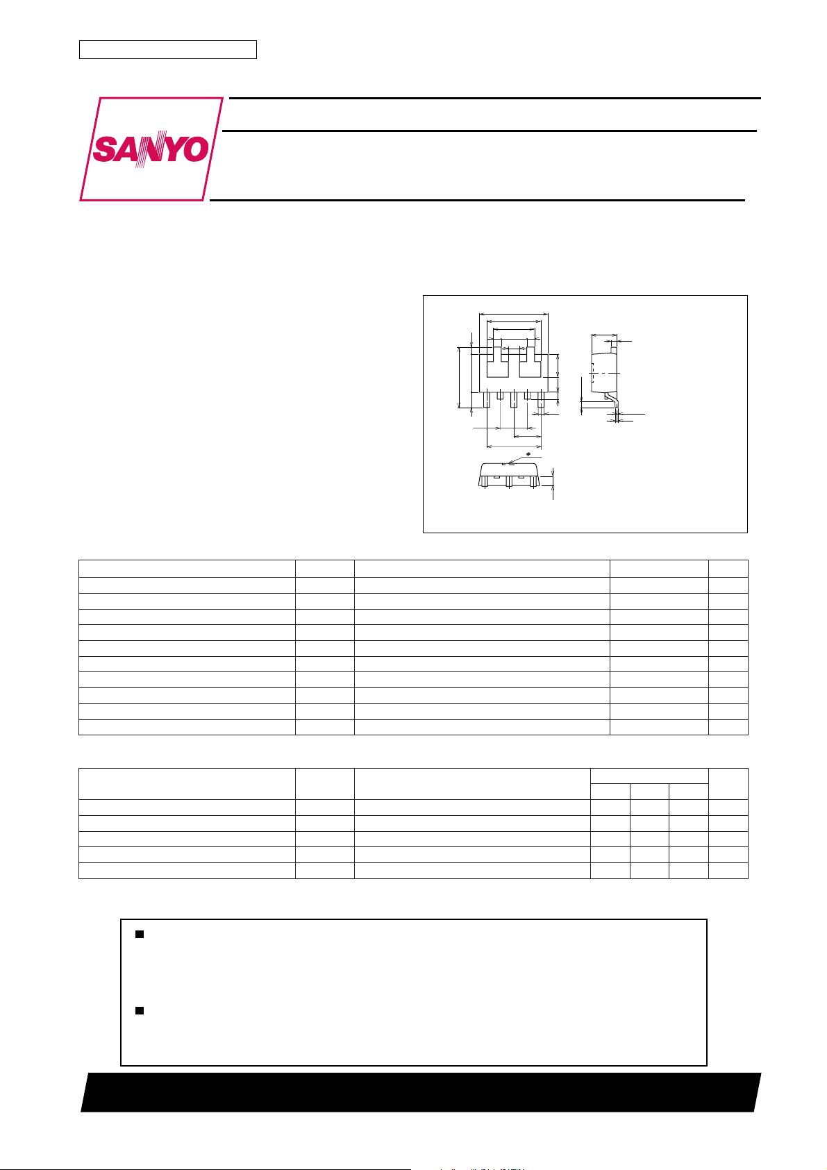
Package Dimensions
unit:mm
2097B
4.5
3.4
2.8
0.5
1.8
0.5
6
1.0
2.5
4.25max
1.0
4
2
5
3
1.75
Mounted on a ceramic board (250mm2×0.8mm) 1unit
Mounted on a ceramic board (250mm2×0.8mm)
1.75
3.5
[FP207]
0.5
7
1.57
0.5
1
0.3
1.2
0.7
1.5
0.4
0.2min
0 to 0.1
0.2
1 : Base 1 (PNP TR)
2 : Collector 1 (PNP TR)
3 : Emitter Common
4 : Collector 2 (NPN TR)
5 : Base 2 (NPN TR)
6 : Collector 2 (NPN TR)
7 : Collector 1 (PNP TR)
SANYO : PCP5 (Top view)
05)–(V
04)–(V
5)–(V
5.1)–(A
3)–(A
003Am
8.0W
1.1W
˚C
˚C
Electrical Characteristics at Ta = 25˚C
retemaraPlobmySsnotidnoC
tnerruCffotuCrotcelloCI
tnerruCffotuCrettimEI
niaGtnerruCCDh
tcudorPhtdiwdnaB-niaGf
ecnaticapaCtuptuOboCV
V
OBC
OBE
EF
T
BC
V
BE
V
EC
V
EC
BC
I,V04)–(=
0=1)–(Aµ
E
I,V3)–(=
0=1)–(Aµ
C
I,V2)–(=
C
I,V2)–(=
C
Am001)–(=001004
Am001)–(=003zHM
zHM1=f,V01)–(=31)81(Fp
nimpytxam
Marking : 207 Continued on next page.
92500TS (KOTO) TA-2925 No.6457–1/5
sgnitaR
tinU
Page 2
FP207
Continued from preceding page.
retemaraPlobmySsnotidnoC
egatloVnoitarutaSrettimE-ot-rotcelloCV
egatloVnoitarutaSrettimE-ot-esaBV
egatloVnwodkaerBesaB-ot-rotcelloCV
egatloVnwodkaerBrettimE-ot-rotcelloCV
egatloVnwodkaerBesaB-ot-rettimEV
emiTNO-nruTt
emiTegarotSt
emiTllaFt
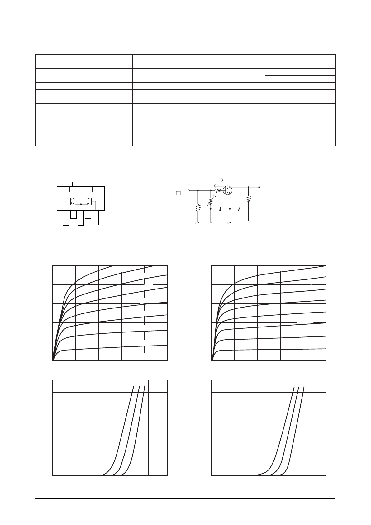
Electrical Connection (Top view) Switching Time Test Circuit
C1 C2
C1 C2
B1 EC B2
EC
EB
no
gts
f
)tas(I
C
)tas(I
C
I
OBC)RB(
C
I
OEC)RB(
C
I
OBE)RB(
E
PW=20µs
D.C.≤1%
I,Am008)–(=
B
I,Am008)–(=
B
I,Aµ01)–(=
E
R,Am1)–(=
EB
I,Aµ01)–(=
C
INPUT
Am04)–(=
Am04)–(=9.0)–(3.1)–(V
0=05)–(V
=∞ 04)–(V
0=5)–(V
tiucriCtseTdeificepseeS
tiucriCtseTdeificepseeS
tiucriCtseTdeificepseeS03)03(08)08(sn
I
B1
I
B2
R
B
V
R
50Ω
(For PNP, the polarity is reversed.)
10IB1= --10IB2= IC=400mA
+
100µF 470µF
+
VCC=25VVBE=--5V
OUTPUT
R
L
sgnitaR
nimpytxam
)3.0–()8.0–(Vm
52.07.0Vm
)05()001(sn
05001sn
)021()022(sn
051072sn
tinU
--1 .0
--0 .8
–A
C
--0 .6
C
--8mA
CE
--7mA
--6mA
--5mA
--4mA
I
-- V
--3mA
--0 .4
--2mA
Collector Current, I
--0 .2
0
0 --1 --2 --3 --4 --5
--1mA
I
B
Collector-to-Emitter Voltage, VCE–V
--1 .6
--1 .4
--1 .2
–A
C
--1 .0
--0 .8
--0 .6
--0 .4
Collector Current, I
--0 .2
IC -- V
VCE= --2V
BE
°C
Ta=75
25°C
°C
--25
[PNP] [NPN]
1.0
I
C
-- V
CE
4.0mA
3.5mA
0.8
–A
C
0.6
3.0mA
2.5mA
2.0mA
25°C
1.5mA
1.0mA
0.5mA
IB=0
°C
--25
0.4
Collector Current, I
0.2
=0
IT01846
[PNP] [NPN]
0
012345
Collector-to-Emitter Voltage, VCE–V
1.6
1.4
1.2
–A
C
1.0
0.8
0.6
0.4
Collector Current, I
0.2
IC -- V
VCE=2V
BE
Ta=75°C
IT01847
0
0 --0.2 --0.4 --0.6 --0.8 --1.2--1.0
Base-to-Emitter Voltage, VBE–V
0
0 0.2 0.4 0.6 0.8 1.21.0
IT01848 IT01849
Base-to-Emitter Voltage, VBE–V
No.6457–2/5
Page 3

1000
FE
100
DC Current Gain, h
100
7
5
3
2
7
5
3
2
10
--0.01
7
FP207
hFE -- I
Ta=75
C
°C
25°C
°C
--25
23 57 23 57 23
--0.1 --1.0
Collector Current, IC–A
Cob -- V
CB
[PNP] [NPN]
VCE= --2V
IT01850 IT01851
[PNP] [NPN]
f=1MHz
1000
FE
100
DC Current Gain, h
hFE -- I
7
5
3
2
7
5
3
2
0.01
7
5
Ta=75
25
--25
2357 2 357 57 2 3
Collector Current, IC–A
Cob -- V
C
VCE=2V
°C
°C
°C
0.1 1.0
CB
f=1MHz
Output Capacitance, Cob – pF
– MHz
T
100
Gain-Bandwidth Product, f
--1000
5
3
2
10
7
5
57
5
3
2
7
5
3
57
7
5
--1 .0
--1 0
23 57
Collector-to-Base Voltage, VCB–V
fT -- I
5723 5723
Collector Current, IC–A
VCE(sat) -- I
--1 0
C
--100 --1000
C
3
2
10
7
Output Capacitance, Cob – pF
5
– MHz
T
100
3
57
7
5
3
2
7
5
23 2357
1.0 10
Collector-to-Base Voltage, VCB–V
fT -- I
C
23
5
IT01852
[PNP] [NPN]
VCE= --2V
Gain-Bandwidth Product, f
3
IT01854
[PNP] [NPN]
IC / IB=20
7
1000
7
5
23 57 23 57
10
Collector Current, IC–A
100 1000
VCE(sat) -- I
C
5
IT01853
VCE=2V
2
IT01855
IC / IB=20
3
(sat) – mV
CE
2
--100
7
5
Collector-to-Emitter
Saturation Voltage, V
3
23 57
--0.01
°C
Ta=75
--25°C
--0 .1
Collector Current, IC–A
25°C
23 57
--1 .0
IT01856
(sat) – mV
3
CE
2
Ta= --25
°C
°C
100
Collector-to-Emitter
Saturation Voltage, V
32
75°C
7
5
0.01
23 57 235757
25
Collector Current, IC–A
0.1 1.0
32
IT01857
No.6457–3/5
Page 4

FP207
5
VBE(sat) -- I
C
[PNP] [NPN]
IC / IB=20
5
VBE(sat) -- I
C
IC / IB=20
3
2
(sat) – V
BE
100
Ta= --25
7
5
Base-to-Emitter
Saturation Voltage, V
3
--0.01
5
3
2
100
7
5
3
2
Switching Time, SW Time – ns
°C
75
23 57 23 57 23
25°C
°C
--0.1 --1.0
Collector Current, IC–A
SW Time -- I
C
IT01858
[PNP] [NPN]
VCC= --25V
IC=20IB1= --20I
t
stg
t
on
t
f
B2
3
2
(sat) – V
BE
1.0
7
5
Base-to-Emitter
Saturation Voltage, V
3
5
Ta= --25
°C
75
57 2 3 57 2 3 57 2 3
0.01 0.1 1.0
Collector Current, IC–A
25°C
°C
SW Time -- I
C
VCC=25V
3
t
2
100
7
5
3
2
Switching Time, SW Time – ns
stg
t
on
t
f
IC=20IB1= --20I
IT01859
B2
10
--0.1
7
5
ICP=3A
3
2
IC=1.5A
–A
1.0
C
7
5
3
2
0.1
Ta=25°C
Collector Current, I
Single pulse
7
5
For PNP, the minus sign is omitted.
1unit
3
Mounted on a ceramic board(250mm
2
57
1.2
1.1
1.0
23 57
Collector Current, IC–A
DC operation
1.0
Collector-to-Emitter Voltage, VCE–V
–W
C
0.8
A S O
10ms
1ms
100ms
2
5723 5723
P
-- Ta
C
Total dissipation
×0.8mm)
10
--1.0
IT01860
IT01862
2
10
0.1
1.0
0.8
(TR2) – W
C
0.6
0.4
0.2
23 57
Collector Current, IC–A
1.0
PC(TR2) -- PC(TR1)
2
IT01861
Collector Dissipation, P
Mounted on a ceramic board(250mm
0
0
0.2 0.4 0.6 0.8 1.0
Collector Dissipation, PC (TR1) – W
2
×0.8mm)
IT01863
0.6
0.4
Collector Dissipation, P
0.2
Mounted on a ceramic board(250mm
0
0 20 40 60 80 100 120 140 160
1unit
2
×0.8mm)
Ambient Temperature, Ta – °C
IT01864
No.6457–4/5
Page 5

FP207
Specifications of any and all SANYO products described or contained herein stipulate the performance,
characteristics, and functions of the described products in the independent state, and are not guarantees
of the performance, characteristics, and functions of the described products as mounted in the customer's
products or equipment. To verify symptoms and states that cannot be evaluated in an independent device,
the customer should always evaluate and test devices mounted in the customer's products or equipment.
SANYO Electric Co., Ltd. strives to supply high-quality high-reliability products. However, any and all
semiconductor products fail with some probability. It is possible that these probabilistic failures could
give rise to accidents or events that could endanger human lives, that could give rise to smoke or fire,
or that could cause damage to other property. When designing equipment, adopt safety measures so
that these kinds of accidents or events cannot occur. Such measures include but are not limited to protective
circuits and error prevention circuits for safe design, redundant design, and structural design.
In the event that any or all SANYO products(including technical data,services) described or
contained herein are controlled under any of applicable local export control laws and regulations,
such products must not be exported without obtaining the export license from the authorities
concerned in accordance with the above law.
No part of this publication may be reproduced or transmitted in any form or by any means, electronic or
mechanical, including photocopying and recording, or any information storage or retrieval system,
or otherwise, without the prior written permission of SANYO Electric Co. , Ltd.
Any and all information described or contained herein are subject to change without notice due to
product/technology improvement, etc. When designing equipment, refer to the "Delivery Specification"
for the SANYO product that you intend to use.
Information (including circuit diagrams and circuit parameters) herein is for example only ; it is not
guaranteed for volume production. SANYO believes information herein is accurate and reliable, but
no guarantees are made or implied regarding its use or any infringements of intellectual property rights
or other rights of third parties.
This catalog provides information as of September, 2000. Specifications and information herein are
subject to change without notice.
PS No.6457–5/5
 Loading...