

Page 1
FODM3062, FODM3063, FODM3082, FODM3083 — 4-Pin Full Pitch Mini-Flat Package Zero-Cross Triac Driver Output Optocouplers
September 2010
FODM3062, FODM3063, FODM3082, FODM3083
4-Pin Full Pitch Mini-Flat Package Zero-Cross
Triac Driver Output Optocouplers
Features
■
dv/dt of 600V/µs guaranteed
Compact 4-pin surface mount package
■
(2.4mm maximum standoff height)
■
Zero voltage crossing
Peak blocking voltage: 600V (FODM306X)
■
800V (FODM308X)
Available in tape and reel quantities of 2500
■
■
C-UL, UL and VDE certifications pending
Applications
■
Solenoid/valve controls
Lighting controls
■
■
Static power switches
AC motor drives
■
■
Temperature controls
■
E.M. contactors
AC motor starters
■
■
Solid state relays
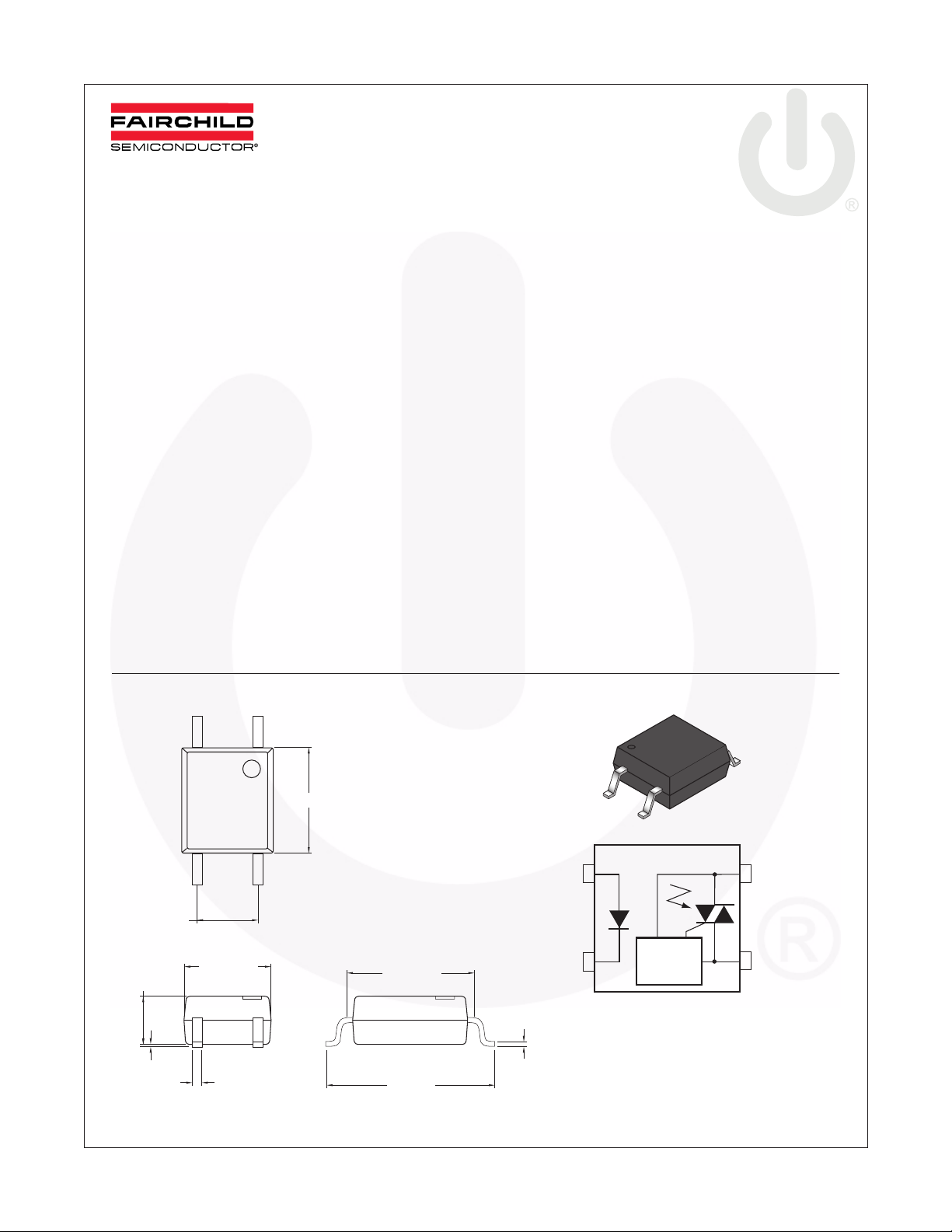
Package Dimensions
Description
The FODM306X and FODM308X series consist of an
infrared emitting diode optically coupled to a monolithic
silicon detector performing the function of a zero voltage
crossing bilateral triac driver, and is housed in a compact
4-pin mini-flat package. The lead pitch is 2.54mm. They
are designed for use with a triac in the interface of logic
systems to equipment powered from 115/240 VAC lines,
such as solid state relays, industrial controls, motors,
solenoids and consumer appliances.
4.40±0.20
ANODE
1
2.54±0.25
ZERO
3.60±0.30
2.00±0.20
0.10±0.10
0.40±0.10
Note:
All dimensions are in millimeters.
©2006 Fairchild Semiconductor Corporation www.fairchildsemi.com
FODM3062, FODM3063, FODM3082, FODM3083 Rev. 1.0.9
5.30±0.30
+0.2
7.00
–0.7
CATHODE
0.20±0.05
2
CROSSING
CIRCUIT
MAIN TERM.
4
3
MAIN TERM.
Page 2

(T
Absolute Maximum Ratings
= 25°C unless otherwise specified)
A
Stresses exceeding the absolute maximum ratings may damage the device. The device may not function or be
operable above the recommended operating conditions and stressing the parts to these levels is not recommended.
In addition, extended exposure to stresses above the recommended operating conditions may affect device reliability.
The absolute maximum ratings are stress ratings only.
Symbol Parameter Rating Units
TOTAL PACKAGE
T
STG
T
OPR
EMITTER
I
F (avg)
I
F (pk)
V
R
P
D
DETECTOR
I
T(RMS)
V
DRM
P
D
Storage Temperature -55 to +150 °C
Operating Temperature -40 to +100 °C
Continuous Forward Current 60 mA
Peak Forward Current (1µs pulse, 300pps.) 1 A
Reverse Input Voltage 6 V
Power Dissipation (No derating required over operating temp. range) 100 mW
On-State RMS Current 70 mA (RMS)
Off-State Output Terminal Voltage FODM3062/FODM3063 600 V
FODM3082/FODM3083 800
Power Dissipation (No derating required over operating temp. range) 300 mW
FODM3062, FODM3063, FODM3082, FODM3083 — 4-Pin Full Pitch Mini-Flat Package Zero-Cross Triac Driver Output Optocouplers
©2006 Fairchild Semiconductor Corporation www.fairchildsemi.com
FODM3062, FODM3063, FODM3082, FODM3083 Rev. 1.0.9 2
Page 3

(T
Electrical Characteristics
= 25°C)
A
Individual Component Characteristics
Symbol Parameter Test Conditions Min. Typ.* Max. Units
EMITTER
V
Input Forward Voltage I
F
I
Reverse Leakage Current V
R
= 30mA 1.5 V
F
= 6V 100 µA
R
DETECTOR
I
DRM1
Peak Blocking Current,
Either Direction
dV/dt Critical Rate of Rise of
Off-State Voltage
Rated V
I
DRM
= 0 (Figure 1)
F
(1)
, I
= 0
F
(2)
600 V/µs
500 nA
Transfer Characteristics
Symbol DC Characteristics Test Conditions Device Min. Typ.* Max. Units
I
V
I
LED Trigger Current Main Terminal
FT
Holding Current,
H
Either Direction
Peak On-State Voltage,
TM
Either Direction
Voltage = 3V
I
= Rated I
F
I
= 100mA peak
TM
FT
(3)
FODM3062 10 mA
FODM3082
FODM3063 5
FODM3083
All 300 µA
,
All 3 V
FODM3062, FODM3063, FODM3082, FODM3083 — 4-Pin Full Pitch Mini-Flat Package Zero-Cross Triac Driver Output Optocouplers
Zero Crossing Characteristics
Symbol Characteristics Test Conditions Device Min. Typ.* Max. Units
V
IH
Inhibit Voltage,
MT1-MT2 Voltage
above which device
will not trigger
IDRM2 Leakage in Inhibit
State
I
= Rated I
F
I
= Rated I
F
FT
Rated VDRM,
Off-State
All 20 V
FT
,
All 2 mA
Isolation Characteristics
Characteristics Test Conditions Symbol Device Min. Typ.* Max. Units
Steady State Isolation
(4)
Voltage
*All typicals at 25°C.
Notes:
1. Test voltage must be applied within dv/dt rating.
2. This is static dv/dt. See Figure 1 for test circuit. Commutating dv/dt is function of the load-driving thyristor(s) only.
3. All devices are guaranteed to trigger at an I
I
lies between max I
F
4. Steady state isolation voltage, V
common, and pins 3 & 4 are common.
(1 Minute)
V
ISO
All 3750 VRMS
R.H. = 40% to 60%
value less than or equal to max I
(10mA for FODM3062/82, 5mA for FODM3063/83) and absolute max I
FT
ISO
F
, is an internal device dielectric breakdown rating. For this test, pins 1 & 2 are
. Therefore, recommended operating
FT
(60 mA).
F
©2006 Fairchild Semiconductor Corporation www.fairchildsemi.com
FODM3062, FODM3063, FODM3082, FODM3083 Rev. 1.0.9 3
Page 4
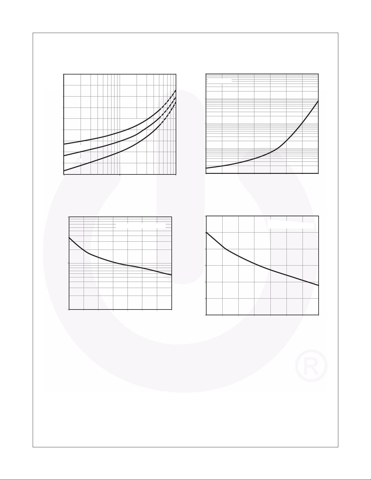
Typical Performance Curves
Fig. 1 LED Forward Voltage vs. Forward Current Fig. 2 Leakage Current vs. Ambient Temperature
1.8
1.7
1000
VDRM = 600V
FODM3062, FODM3063, FODM3082, FODM3083 — 4-Pin Full Pitch Mini-Flat Package Zero-Cross Triac Driver Output Optocouplers
1.6
1.5
1.4
1.3
1.2
- FORWARD VOLTAGE (V)
F
V
TA = 25°C
1.1
TA = 100°C
1.0
0.9
110100
IF - FORWARD CURRENT (mA)
TA = -40°C
Fig. 3 Holding Current vs. Ambient Temperature Fig. 4 Trigger Current vs. Ambient Temperature
10
NORMALIZED TO TA = 25°C
1.0
100
10
- LEAKAGE CURRENT (nA)
1
DRM
I
0.1
-40 -20 0 20 406080100
TA - AMBIENT TEMPERATURE (°C)
1.6
1.4
1.2
1.0
= 3V
V
TM
NORMALIZED TO T
= 25°C
A
0.8
- HOLDING CURRENT (NORMALIZED)
H
I
0.1
-40 -20 100
020406080
TA - AMBIENT TEMPERATURE (°C)
- TRIGGER CURRENT (NORMALIZED)
0.6
FT
I
0.8
-40 -20 0 20 40 60 80
TA - AMBIENT TEMPERATURE (°C)
100
©2006 Fairchild Semiconductor Corporation www.fairchildsemi.com
FODM3062, FODM3063, FODM3082, FODM3083 Rev. 1.0.9 4
Page 5

FODM3062, FODM3063, FODM3082, FODM3083 — 4-Pin Full Pitch Mini-Flat Package Zero-Cross Triac Driver Output Optocouplers
Typical Performance Curves
(Continued)
Fig. 5 LED Current Required to Trigger vs. LED Pulse Width Fig. 6 Off-State Output Terminal Voltage vs. Ambient Temperature
12
T= 25°C
A
10
8
6
4
- LED TRIGGER CURRENT (NORMALIZED)
2
FT
I
0
PWIN - LED TRIGGER PULSE WIDTH (°C)
T
A
>> 100µsNORMALIZED TO PW
IN
100101
1.4
NORMALIZED TO T = 25°C
1.3
1.2
1.1
1.0
(NORMALIZED)
0.9
0.8
- OFF-STATE OUTPUT TERMINAL VOLTAGE
0.7
DRM
V
0.6
-40 -20
A
020406080100
TA - AMBIENT TEMPERATURE (°C)
Fig. 7 On-State Characteristics
800
TA = 25°C
600
400
200
0
-200
- ON-STATE CURRENT (mA)
TM
I
-400
-600
-800
-4 -3 -2 -1 01234
VTM - ON-STATE VOLTAGE (V)
©2006 Fairchild Semiconductor Corporation www.fairchildsemi.com
FODM3062, FODM3063, FODM3082, FODM3083 Rev. 1.0.9 5
Page 6
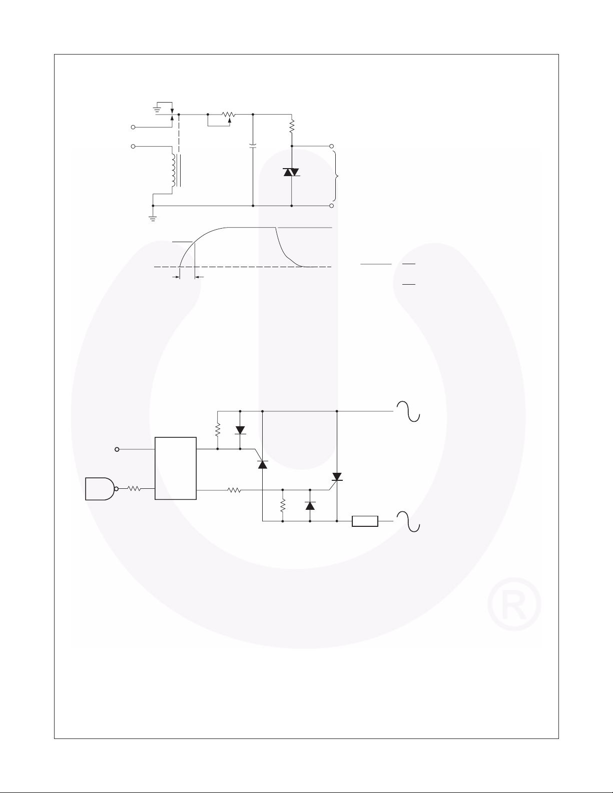
Typical Applications
FODM3062, FODM3063, FODM3082, FODM3083 — 4-Pin Full Pitch Mini-Flat Package Zero-Cross Triac Driver Output Optocouplers
800V (FODM3082)
(FODM3083)
600V (FODM3062)
(FODM3063)
Note:
This optoisolator should not be used to drive a load directly. It is intended to be a trigger device only.
Vdc
PULSE
INPUT
APPLIED VOLTAGE
WAVEFORM
0 VOLTS
R
TEST
MERCURY
WETTED
RELAY
378V (FODM3062, FODM3063)
504V (FODM3082, FODM3083)
τ
RC
R = 10 kΩ
C
TEST
D.U. T.D.U. T.
Figure 8. Static dv/dt Test Circuit
X100
SCOPE
PROBE
1. The mercury wetted relay provides a high speed repeated
pulse to the D.U.T.
2. 100x scope probes are used, to allow high speeds and
voltages.
3. The worst-case condition for static dv/dt is established by
triggering the D.U.T. with a normal LED input current, then
removing the current. The variable RTEST allows the dv/dt
to be gradually increased until the D.U.T. continues to trigger
in response to the applied voltage pulse, even after the LED
current has been removed. The dv/dt is then decreased until
the D.U.T. stops triggering. tRC is measured at this point
and recorded.
V
=
= 800V (FODM3082, FODM3083)
max
= 600V (FODM3062, FODM3063)
dv/dt =
0.63 V
τ
RC
max
378
=
(FODM3062, FODM3063)
τ
RC
504
(FODM3082, FODM3083)
=
τ
RC
R1 D1
V
CC
Note:
This optoisolator should not be used to drive a load directly. It is intended to be a trigger device only.
1
FODM3062
FODM3063
FODM3082
R
FODM3083
in
2
4
SCR
360 Ω
3
R2 D2
SCR
LOAD
Figure 9. Inverse-Parallel SCR Driver Circuit (240VAC)
240 VAC
Suggested method of firing two, back-to-back
SCR’s, with a Fairchild triac driver. Diodes can
be 1N4001; resistors, R1 and R2, are optional
330 ohms.
©2006 Fairchild Semiconductor Corporation www.fairchildsemi.com
FODM3062, FODM3063, FODM3082, FODM3083 Rev. 1.0.9 6
Page 7
Determining the Power Rating of the Series Resistors Used in a Zero-Cross
Opto-TRIAC Driver Application
The following will present the calculations for
determining the power dissipation of the current
limiting resistors found in an opto-TRIAC driver
interface.
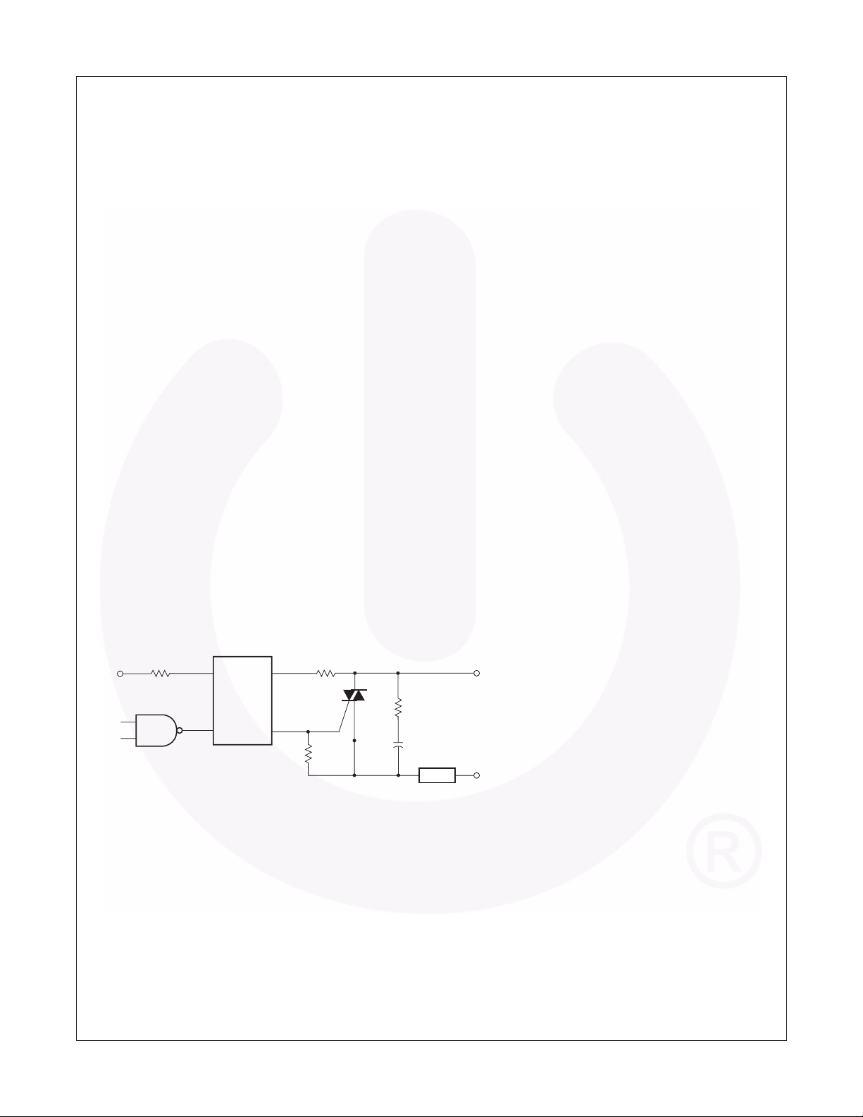
Figure 10 shows a typical circuit to drive a sensitive
gate four quadrant power TRIAC. This figure provides
typical resistor values for a zero line cross detecting
opto-TRIAC when operated from a mains voltage of
20V to 240V. The wattage rating for each resistor is
not given because their dissipation is dependent upon
characteristics of the power TRIAC being driven.
Recall that the opto-TRIAC is used to trigger a four
quadrant power TRIAC. Please note that these optoTRIACs are not recommended for driving
“snubberless” three quadrant power TRIACs.
Under normal operation, the opto-TRIAC will fire when
the mains voltage is lower than the minimum inhibit
trigger voltage, and the LED is driven at a current
greater than the maximum LED trigger current. As an
example for the FODM3063, the LED trigger current
should be greater than 5mA, and the mains voltage is
less than 10V peak. The inhibit voltage has a typical
range of 10V minimum and 20V maximum. This
means that if a sufficient LED current is flowing when
the mains voltage is less than 10V, the device will fire.
If a trigger appears between 10V and 20V, the device
may fire. If the trigger occurs after the mains voltage
has reached 20Vpeak, the device will not fire.
The power dissipated from resistors placed in series
with the opto-TRIAC and the gate of the power TRIAC
is much smaller than one would expect. These current
handling components only conduct current when the
mains voltage is less than the maximum inhibit
voltage. If the opto-TRIAC is triggered when the mains
voltage is greater than the inhibit voltage, only the
TRIAC leakage current will flow. The power dissipation
in a 360Ω resistor shown in Figure 10 is the product of
the resistance (360Ω) times the square of the current
sum of main TRIAC’s gate current plus the current
flowing gate to the MT2 resistor connection (330Ω).
This power calculation is further modified by the duty
factor of the duration for this current flow. The duty
factor is the ratio of the turn-on time of the main TRIAC
to the sine of the single cycle time. Assuming a main
TRIAC turn-on time of 50µs and a 60Hz mains
voltage, the duty cycle is approximately 0.6%.
The opto-TRIAC only conducts current while triggering
the main TRIAC. Once the main TRIAC fires, its onstate voltage is typically lower than the on-state
sustaining voltage of the opto-TRIAC. Thus, once the
main TRIAC fires, the opto-TRIAC is often shunted off.
This situation results in very low power dissipation for
both the 360Ω and 330Ω resistors, when driving a
traditional four quadrant power TRIAC.
If a three quadrant “snubberless” TRIAC is driven by
the opto-TRIAC, the calculations are different. When
the main power TRIAC is driving a high power factor
(resistive) load, it shuts off during the fourth quadrant.
FODM3062, FODM3063, FODM3082, FODM3083 — 4-Pin Full Pitch Mini-Flat Package Zero-Cross Triac Driver Output Optocouplers
R
in
V
CC
For highly inductive loads (power factor < 0.5), change this value to 360 ohms.
*
©2006 Fairchild Semiconductor Corporation www.fairchildsemi.com
FODM3062, FODM3063, FODM3082, FODM3083 Rev. 1.0.9 7
1
2
FODM3062
FODM3063
FODM3082
FODM3083
360 Ω
4
39*
3
330
Figure 10. Hot-Line Switching Application Circuit
0.01
LOAD
HOT
240 VAC
NEUTRAL
Typical circuit for use when hot line switching of 240VAC
is required. In this circuit the “hot” side of the line is
switched and the load connected to the cold or neutral
side. The load may be connected to either the neutral or
hot line.
R
is calculated so that IF is equal to the rated IFT of the
in
part, 5mA for the FODM3063/83 and 10mA for the
FODM3062/82. The 39Ω resistor and 0.01µF capacitor are
for snubbing of the triac and may or may not be necessary
depending upon the particular triac and load used.
Page 8

FODM3062, FODM3063, FODM3082, FODM3083 — 4-Pin Full Pitch Mini-Flat Package Zero-Cross Triac Driver Output Optocouplers
If sufficient holding current is still flowing through the
opto-TRIAC, the opto-TRIAC will turn-on and attempt
to carry the power TRIACs load. This situation typically
causes the opto-TRIAC to operate beyond its
maximum current rating, and product and resistor
failures typically result. For this reason, using an optoTRIAC to drive a three quadrant “snubberless” power
TRIAC is not recommended.
Power in the 360Ω resistor, when driving a sensitive
gate 4 quadrant power TRIAC:
I
= 20mA
GT
V
= 1.5V
GT
DF = 0.6%
P = (I
GT
+V
GT
/
P = (20mA + 1.5
330 Ω )
/
330 Ω )
2
x 360 Ω x DF
2
*x 360 Ω x 0.6% = 1.3mW
A 1/4 watt resistor is more than adequate for both the
360 Ω and 330 Ω resistors.
The real power in the snubber resistor is based upon
the integral of the power transient present when the
load commutes. A fast commuting transient may allow
a peak current of 4A to 8A in the snubbing filter.
For best results, the capacitor should be a nonpolarized AC unit with a low ESR. The 39Ω series
resistor sets a time constant and limits the peak
current. For a resistive load with a power factor near
unity, the commutating transients will be small. This
results in a very small peak current given the 0.01µF
capacitor’s reactance. Normally, for factional horsepower reactive loads, the resistor found in the snubber
circuit will have a power rating from 1/2W to 2W. The
resistor should be a low inductance type to adequately
filter the high frequency transients.
©2006 Fairchild Semiconductor Corporation www.fairchildsemi.com
FODM3062, FODM3063, FODM3082, FODM3083 Rev. 1.0.9 8
Page 9
Ordering Information
Option Description
No option Bulk (100 units/tube)
V VDE Approved
R2 Tape and Reel (2500 units)
R2V Tape and Reel (2500 units) and VDE Approved
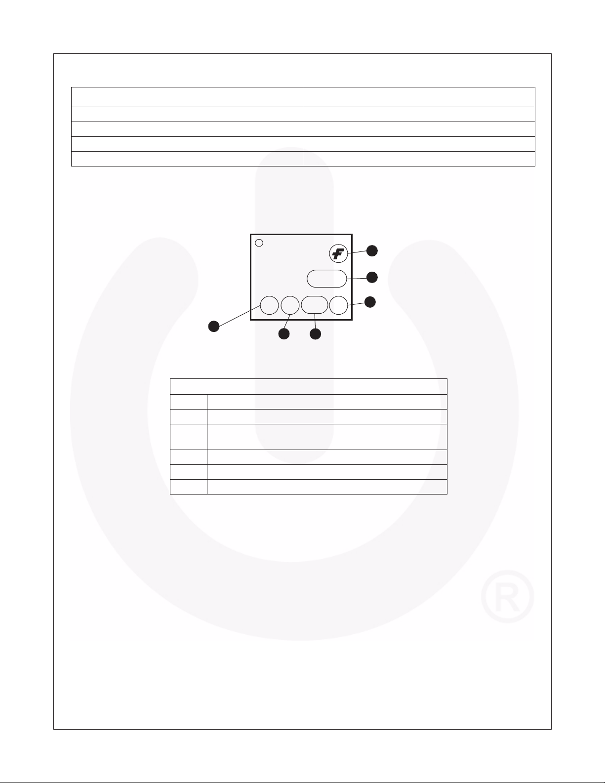
Marking Information
FODM3062, FODM3063, FODM3082, FODM3083 — 4-Pin Full Pitch Mini-Flat Package Zero-Cross Triac Driver Output Optocouplers
1
3063
XVR
YY
3
4
5
2
6
Definitions
1Fairchild logo
2Device number
3 VDE mark (Note: Only appears on parts ordered with VDE
option – See order entry table)
4 One digit year code
5Two digit work week ranging from ‘01’ to ‘53’
6 Assembly package code
©2006 Fairchild Semiconductor Corporation www.fairchildsemi.com
FODM3062, FODM3063, FODM3082, FODM3083 Rev. 1.0.9 9
Page 10
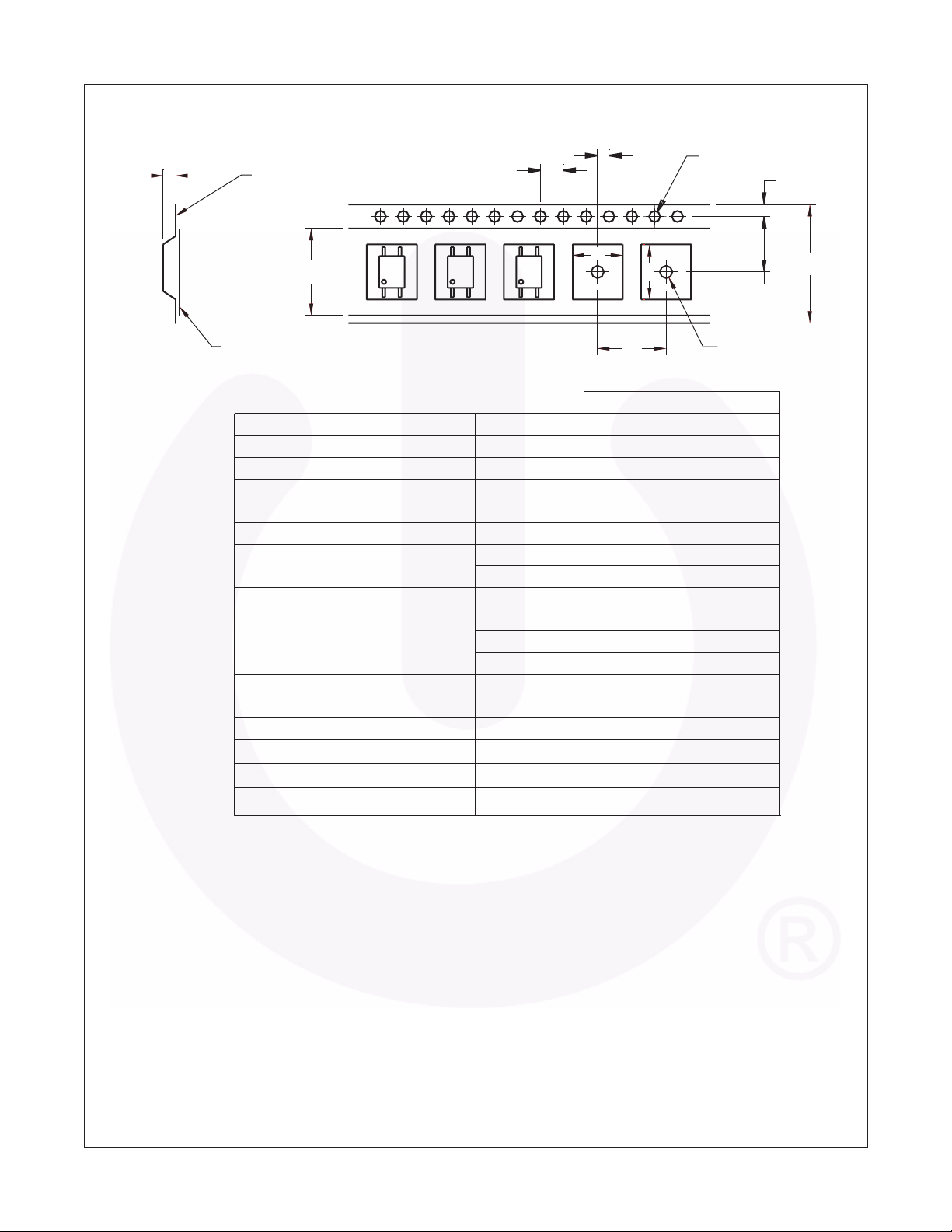
Tape and Reel Information
FODM3062, FODM3063, FODM3082, FODM3083 — 4-Pin Full Pitch Mini-Flat Package Zero-Cross Triac Driver Output Optocouplers
K
t
0
d
Tape
Tape
Sprocket Hole
Sprocket Hole Dia.
Sprocket Hole Locatio
Pocket Location
Pocket Pitch
Pocket Dim
Poc
Cover Tape Width
o
ver Ta
C
Max. C
Devices Per Reel
W
Width
Thickness
ket Hole
pe Thickness
o
mp
1
Description
Pitch
n
e
nsion
Dia.
n
ent Rotatio
o
n
or Tilt
P
0
Symbol
W
t
P
0
D
0
E
F
P
2
P
A
0
B
0
K
0
D
1
W
1
d
P
2
D
0
E
A
0
P
B
0
2.54 Pitch
Dimensions
±
0.4
12.00
0.35
±
0.02
4.00
±
0.20
1.55
±
0.20
1.75
±
0.20
5.50
±
0.20
2.00
±
0.20
00
20
8.
±
0.
4.75
±
0.20
7.30
±
0.20
2.30
±
0.20
1.55
±
0.20
9.20
±
0.02
0.065
a
x
20°
m
0
250
F
D
1
W
Re
©2006 Fairchild Semiconductor Corporation www.fairchildsemi.com
FODM3062, FODM3063, FODM3082, FODM3083 Rev. 1.0.9 10
330 m
m
(13")
e
ter
m
Dia
el
Page 11
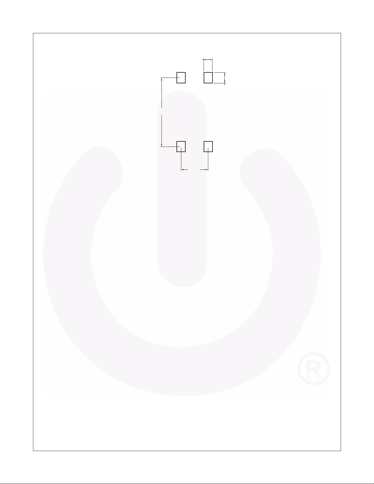
Footprint Drawing for PCB Layout
6.50
0.80
2.54
1.00
FODM3062, FODM3063, FODM3082, FODM3083 — 4-Pin Full Pitch Mini-Flat Package Zero-Cross Triac Driver Output Optocouplers
Note:
All dimensions are in mm.
©2006 Fairchild Semiconductor Corporation www.fairchildsemi.com
FODM3062, FODM3063, FODM3082, FODM3083 Rev. 1.0.9 11
Page 12
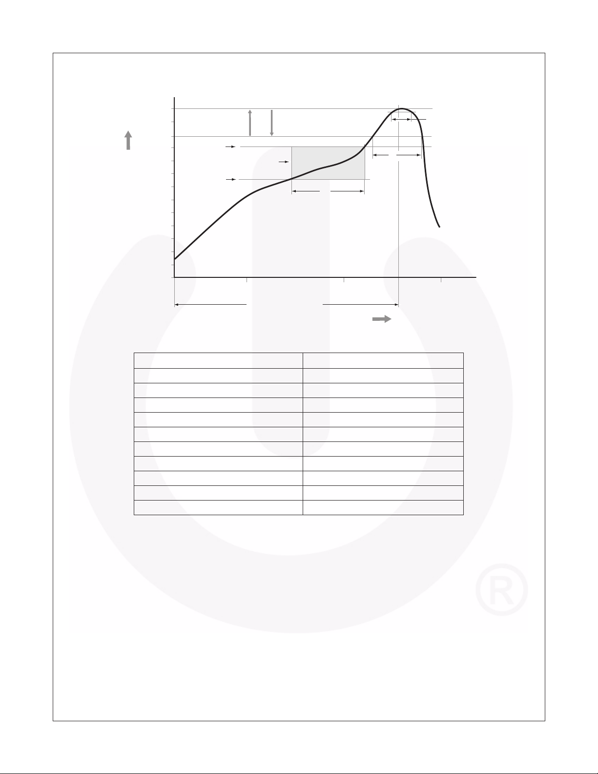
Reflow Profile
FODM3062, FODM3063, FODM3082, FODM3083 — 4-Pin Full Pitch Mini-Flat Package Zero-Cross Triac Driver Output Optocouplers
Max. Ramp-up Rate = 3°C/S
Max. Ramp-down Rate = 6°C/S
Ts ma x
Preheat Area
Ts mi n
t
L
t
s
260
240
220
200
180
160
140
120
T
P
T
L
100
80
60
Temperature (°C)
40
20
0
120
240 360
Time 25°C to Peak
Time (seconds)
Profile Feature Pb-Free Assembly Profile
Temperature Min. (Tsmin) 150°C
Temperature Max. (Tsmax) 200°C
Time (t
Ramp-up Rate (t
Liquidous Temperature (T
Time (t
Peak Body Package Temperature 260°C +0°C / –5°C
Time (t
Ramp-down Rate (T
Time 25°C to Peak Temperature 8 minutes max.
) from (Tsmin to Tsmax) 60–120 seconds
S
to t
) 3°C/second max.
L
P
) 217°C
L
) Maintained Above (T
L
) within 5°C of 260°C 30 seconds
P
to T
P
) 60–150 seconds
L
) 6°C/second max.
L
t
P
©2006 Fairchild Semiconductor Corporation www.fairchildsemi.com
FODM3062, FODM3063, FODM3082, FODM3083 Rev. 1.0.9 12
Page 13

TRADEMARKS
®
The following includes registered and unregistered trademarks and service marks, owned by Fairchild Semiconductor and/or its global subsidiaries,andisnot
intended to be an exhaustive list of all such trademarks.
AccuPower™
Auto-SPM™
Build it Now™
CorePLUS™
CorePOWER™
CROSSVOLT™
CTL™
Current Transfer Logic™
DEUXPEED
Dual Cool™
EcoSPARK
EfficientMax™
®
®
n
ESBC™
F-PFS™
®
FRFET
Global Power Resource
Green FPS™
Green FPS™ e-Series™
Gmax™
GTO™
IntelliMAX™
ISOPLANAR™
MegaBuck™
MICROCOUPLER™
MicroFET™
MicroPak™
MicroPak2™
®
Fairchild
Fairchild Semiconductor
FACT Quiet Series™
®
FACT
®
FAST
FastvCore™
FETBench™
FlashWriter
®
*
FPS™
®
MillerDrive™
MotionMax™
Motion-SPM™
OptoHiT™
OPTOLOGIC
OPTOPLANAR
®
PDP SPM™
®
Power-SPM™
SM
PowerTrench
PowerXS™
Programmable Active Droop™
QFET
QS™
Quiet Series™
RapidConfigure™
Saving our world, 1mW/W/kW at a time™
SignalWise™
SmartMax™
SMART START™
SPM
STEALTH™
SuperFET™
®
The Power Franchise
®
TinyBoost™
TinyBuck™
™
TinyCalc™
TinyLogic
TINYOPTO™
TinyPower™
TinyPWM™
TinyWire™
®
TriFault Detect™
TRUECURRENT™*
" SerDes™
SuperSOT™-3
SuperSOT™-6
®
SuperSOT™-8
SupreMOS
®
SyncFET™
Sync-Lock™
UHC
Ultra FRFET™
UniFET™
VCX™
VisualMax™
XS™
®
*
®
®
®
* Trademarks of System General Corporation, used under license by Fairchild Semiconductor.
DISCLAIMER
FAIRCHILD SEMICONDUCTOR RESERVES THE RIGHT TO MAKE CHANGES WITHOUT FURTHER NOTICE TO ANY PRODUCTS HEREIN TO IMPROVE
RELIABILITY, FUNCTION, OR DESIGN. FAIRCHILD DOES NOT ASSUME ANY LIABILITY ARISING OUT OF THE APPLICATION OR USE OF ANY PRODUCT
OR CIRCUIT DESCRIBED HEREIN; NEITHER DOES IT CONVEY ANY LICENSE UNDER ITS PATENT RIGHTS, NOR THE RIGHTS OF OTHERS. THESE
SPECIFICATIONS DO NOT EXPAND THE TERMS OF FAIRCHILD’S WORLDWIDE TERMS AND CONDITIONS, SPECIFICALLY THE WARRANTY THEREIN,
WHICH COVERS THESE PRODUCTS.
LIFE SUPPORT POLICY
FAIRCHILD’S PRODUCTS ARE NOT AUTHORIZED FOR USE AS CRITICAL COMPONENTS IN LIFE SUPPORT DEVICES OR SYSTEMS WITHOUT THE
EXPRESS WRITTEN APPROVAL OF FAIRCHILD SEMICONDUCTOR CORPORATION.
As used herein:
1. Life support devices or systems are devices or systems which, (a)
are intended for surgical implant into the body or (b) support or
sustain life, and (c) whose failure to perform when properly used in
accordance with instructions for use provided in the labeling, can be
reasonably expected to result in a significant injury of the user.
2. A critical component in any component of a life support, device, or
system whose failure to perform can be reasonably expected to
cause the failure of the life support device or system, or to affect its
safety or effectiveness.
ANTI-C OUNTERFEITING POLICY
Fairchild Semiconductor Corporation's Anti-Counterfeiting Policy. Fairchild's Anti-Counterfeiting Policy is also stated on ourexternal website, www.fairchildsemi.com,
under Sales Support.
Counterfeiting of semiconductor parts is a growing problem in the industry. All manufacturers of semiconductor products are experiencing counterfeiting of their
parts. Customers who inadvertently purchase counterfeit parts experience many problems such as loss of brand reputation, substandard performance,failed
applications, and increased cost of production and manufacturing delays. Fairchild is taking strong measures to protect ourselves and our customersfromthe
proliferation of counterfeit parts. Fairchild strongly encourages customers to purchase Fairchild parts either directly from Fairchild or from Authorized Fairchild
Distributors who are listed by country on our web page cited above. Products customers buy either from Fairchild directly or from Authorized FairchildDistributors
are genuine parts, have full traceability, meet Fairchild's quality standards for handling and storage and provide access to Fairchild's full range of up-to-date technical
and product information. Fairchild and our Authorized Distributors will stand behind all warranties and will appropriately address any warranty issues that may arise.
Fairchild will not provide any warranty coverage or other assistance for parts bought from Unauthorized Sources. Fairchild is committed to combat this global
problem and encourage our customers to do their part in stopping this practice by buying direct or from authorized distributors.
PRODUCT STATUS DEFINITIONS
Definition of Terms
Datasheet
Identification
Advance Information Formative / In Design
Preliminary First Production
No Identification Needed Full Production
Obsolete Not In Production
Product Status Definition
Datasheet contains the design specifications for product development. Specifications may change
in any manner without notice.
Datasheet contains preliminary data; supplementary data will be published at a later date. Fairchild
Semiconductor reserves the right to make changes at any time without notice to improve design.
Datasheet contains final specifications. Fairchild Semiconductor reserves the right to make
changes at any time without notice to improve the design.
Datasheet contains specifications on a product that is discontinued by Fairchild Semiconductor.
The datasheet is for reference information only.
Rev. I49
©2006 Fairchild Semiconductor Corporation www.fairchildsemi.com
FODM3062, FODM3063, FODM3082, FODM3083 Rev. 1.0.9 13
FODM3062, FODM3063, FODM3082, FODM3083 — 4-Pin Full Pitch Mini-Flat Package Zero-Cross Triac Driver Output Optocouplers
 Loading...