

Page 1
FOD8321 — 2.5A Output Current, Gate Drive Optocoupler in Optoplanar
May 2012
FOD8321
2.5A Output Current, Gate Drive Optocoupler in
®
Optoplanar
Wide Body SOP 5-Pin
Features
Fairchild’s Optoplanar
■
provides reliable and high voltage insulation with
greater than 8mm creepage and clearance distance,
and 0.5mm internal insulation distance while still
offering a compact footprint
2.5A output current driving capability for medium
■
power IGBT/MOSFET
– Use of P-Channel MOSFETs at output stage
enables output voltage swing close to the supply
rail
■
20kV/µs Minimum Common Mode Rejection
Wide Supply Voltage range from 15V to 30V
■
■
Fast Switching Speed over full operating temperature
range
– 500ns max. propagation delay
– 300ns max. pulse width distortion
UnderVoltage LockOut (UVLO) with hysteresis
■
■
Extended industrial temperate range, -40 to 100°C
temperature range
■
Safety and regulatory approvals
– UL1577, 5,000V
– DIN EN/IEC60747-5-5, 1,414V peak working
insulation voltage
®
packaging technology
for 1 min.
RMS
Applications
■
AC and brushless DC motor drives
Industrial inverter
■
■
Uninterruptible power supply
Induction heating
■
■
Isolated IGBT/Power MOSFET gate drive
Description
The FOD8321 is a 2.5A Output Current Gate Drive
Optocoupler, capable of driving medium power IGBT/
MOSFETs. It is ideally suited for fast switching driving of
power IGBT and MOSFETs used in motor control
inverter applications, and high performance power
systems.
It utilizes Fairchild’s coplanar packaging technology,
Optoplanar
high insulation voltage and high noise immunity.
It consists of a aluminum gallium arsenide (AlGaAs) light
emitting diode optically coupled to an integrated circuit
with a high-speed driver for push-pull MOSFET output
stage. The device is housed in a wide body 5-pin small
outline plastic package.
®
, and optimized IC design to achieve reliably
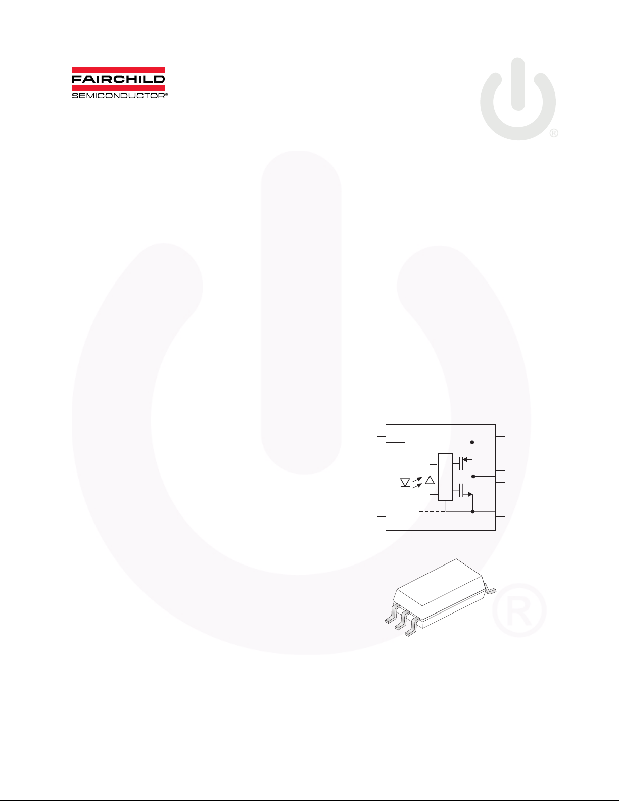
Functional Schematic
ANODE
CATHODE V
1
3
V
6
DD
5
V
O
4
SS
®
Wide Body SOP 5-Pin
Related Resources
■
FOD3120, High Noise Immunity, 2.5A Output Current,
Gate Drive Optocoupler Datasheet
©2010 Fairchild Semiconductor Corporation www.fairchildsemi.com
FOD8321 Rev. 1.0.4
Page 2
Truth Table
V
V
DD–
LED
Off 0V to 30V 0V to 30V Low
On 0V to 11.5V 0V to 10V Low
On 11.5V to 14.5V 10V to 13V Transition
On 14.5V to 30V 13V to 30V High
“Positive Going”
SS
(Turn-on)
V
DD–
V
“Positive Going”
SS
(Turn-off)
Pin Definitions
Pin # Name Description
1 Anode LED Anode
3 Cathode LED Cathode
4V
5V
6V
SS
O
DD
Negative Supply Voltage
Output Voltage
Positive Supply voltage
FOD8321 — 2.5A Output Current, Gate Drive Optocoupler in Optoplanar
V
O
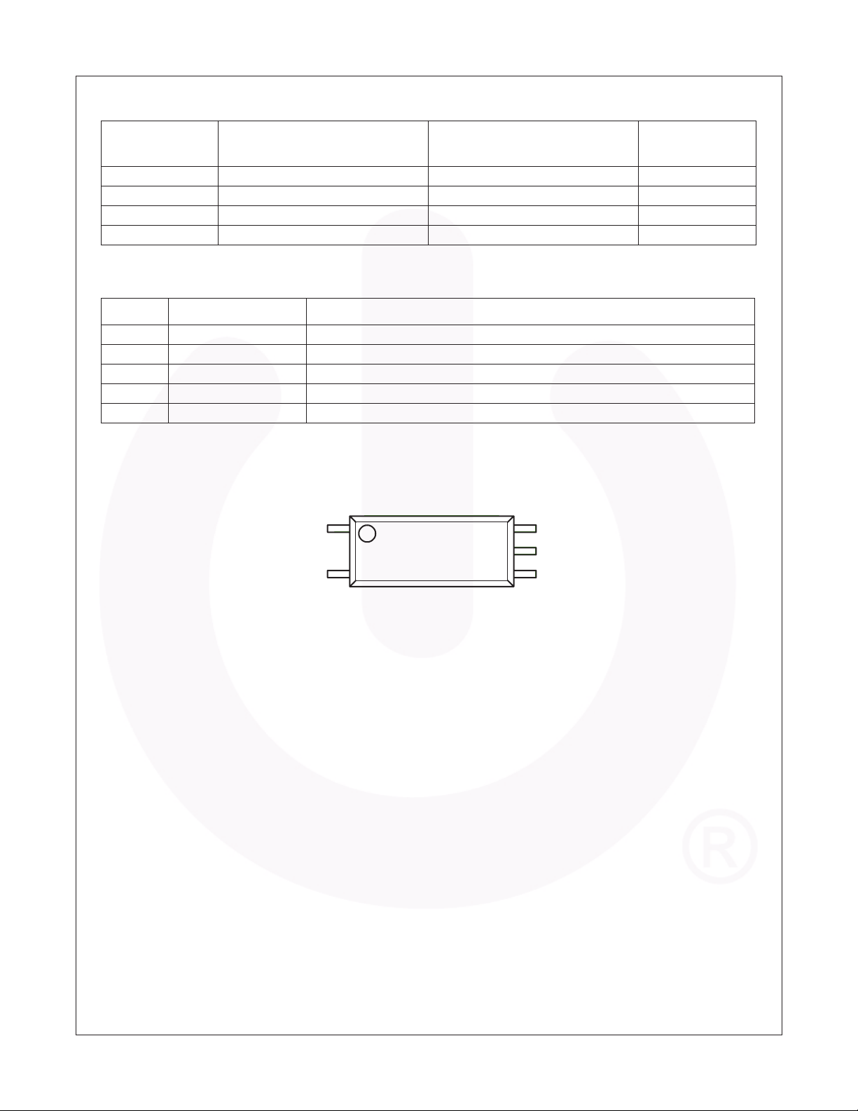
Pin Configuration
ANODE
CATHODE
1
3
6
V
DD
5
V
O
4
V
SS
®
Wide Body SOP 5-Pin
©2010 Fairchild Semiconductor Corporation www.fairchildsemi.com
FOD8321 Rev. 1.0.4 2
Page 3
Safety and Insulation Ratings
As per DIN EN/IEC60747-5-5. This optocoupler is suitable for “safe electrical insulation” only within the safety limit
data. Compliance with the safety ratings shall be ensured by means of protective circuits.
Symbol Parameter Min. Typ. Max. Unit
Pollution Degree (DIN VDE 0110/1.89) 2
CTI Comparative Tracking Index 175
V
PR
V
IORM
V
IOTM
External Creepage 8.0 mm
External Clearance 8.0 mm
Insulation Thickness 0.5 mm
T
S
I
S,INPUT
P
S,OUTPUT
R
IO
Installation Classifications per DIN VDE 0110/1.89 Table 1
For Rated Mains Voltage < 150Vrms I–IV
For Rated Mains Voltage < 300Vrms I–IV
For Rated Mains Voltage < 450Vrms I–IIII
For Rated Mains Voltage < 600Vrms I–III
Climatic Classification 40/100/21
Input to Output Test Voltage, Method b,
V
x 1.875 = V
IORM
t
= 1 sec., Partial Discharge < 5pC
m
, 100% Production Test with
PR
Input to Output Test Voltage, Method a,
V
x 1.5 = V
IORM
t
= 60 sec.,Partial Discharge < 5 pC
m
, Type and Sample Test with
PR
Max Working Insulation Voltage 1,414 V
Highest Allowable Over Voltage 6000 V
2651
2121
peak
peak
Safety Limit Values – Maximum Values Allowed in the
Event of a Failure
Case Temperature 150 °C
Input Current 200 mA
Output Power 600 mW
Insulation Resistance at T
, V
= 500V 10
S
IO
9
Ω
FOD8321 — 2.5A Output Current, Gate Drive Optocoupler in Optoplanar
®
Wide Body SOP 5-Pin
©2010 Fairchild Semiconductor Corporation www.fairchildsemi.com
FOD8321 Rev. 1.0.4 3
Page 4
FOD8321 — 2.5A Output Current, Gate Drive Optocoupler in Optoplanar
Absolute Maximum Ratings
(T
= 25ºC unless otherwise specified)
A
Stresses exceeding the absolute maximum ratings may damage the device. The device may not function or be
operable above the recommended operating conditions and stressing the parts to these levels is not recommended.
In addition, extended exposure to stresses above the recommended operating conditions may affect device reliability.
The absolute maximum ratings are stress ratings only.
Symbol Parameter Value Units
T
STG
T
OPR
T
J
T
SOL
I
F(AVG)
F
V
R
I
O(PEAK)
V
DD
V
O(PEAK)
, t
t
R(IN)
F(IN)
PD
I
PD
O
Notes:
1. Maximum pulse width = 10µs, maximum duty cycle = 0.2%.
2.
No derating required across operating temperature range.
3.
Derate linearly from 25°C at a rate of 5.2mW/°C
4.
Functional operation under these conditions is not implied. Permanent damage may occur if the device is subjected
to conditions outside these ratings.
Storage Temperature
Operating Temperature
Junction Temperature
Lead Solder Temperature (Refer to Reflow Temperature
Profile)
Average Input Current
Operating Frequency
Reverse Input Voltage
Peak Output Current
(1)
Supply Voltage
Peak Output Voltage
Input Signal Rise and Fall Time
Input Power Dissipation
Output Power Dissipation
(2)(4)
(3)(4)
-40 to +125 °C
-40 to +100 °C
-40 to +125 °C
260 for 10 sec °C
25 mA
50 kHz
5.0 V
3.0 A
0 to 35 V
0 to V
DD
V
500 ns
45 mW
500 mW
Recommended Operating Conditions
The Recommended Operating Conditions table defines the conditions for actual device operation. Recommended
operating conditions are specified to ensure optimal performance to the datasheet specifications. Fairchild does not
recommend exceeding them or designing to absolute maximum ratings.
Symbol Parameter Min. Max. Unit
V
T
– V
DD
I
F(ON)
V
F(OFF)
A
Ambient Operating Temperature
Supply Voltage
SS
Input Current (ON)
Input Voltage (OFF)
-40 100 °C
16 30 V
10 16 mA
0 0.8 V
®
Wide Body SOP 5-Pin
©2010 Fairchild Semiconductor Corporation www.fairchildsemi.com
FOD8321 Rev. 1.0.4 4
Page 5
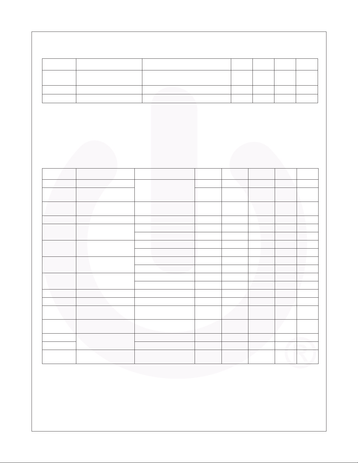
Isolation Characteristics
Apply over all recommended conditions, typical value is measured at T
Symbol Parameter Conditions Min. Typ. Max. Units
= 25ºC
A
≤
Ω
FOD8321 — 2.5A Output Current, Gate Drive Optocoupler in Optoplanar
V
ISO
R
ISO
C
ISO
Input-Output Isolation
Voltage
Isolation Resistance V
Isolation Capacitance V
T
= 25ºC, R.H. < 50%, t = 1.0min,
A
I
20µA, 50Hz
I-O
= 500V
I-O
= 0V, Freq = 1.0MHz
I-O
(5)(6)
(5)
(6)
5,000 V
11
10
1pF
Notes:
5. Device is considered a two terminal device: Pins 1 and 3 are shorted together and Pins 4, 5 and 6 are shorted
together.
6. 5,000 VAC
for 1 minute duration is equivalent to 6,000 VAC
RMS
for 1 second duration.
RMS
Electrical Characteristics
Apply over all recommended conditions, typical value is measured at V
otherwise specified.
Symbol Parameter Conditions Min. Typ. Max. Units Figure
V
F
Δ(VF / TA) Temperature Coefficient of
BV
C
IN
I
OH
I
OL
V
OH
V
OL
I
DDH
I
DDL
I
FLH
V
FHL
V
UVLO+
V
UVLO-
UVLO
Input Forward Voltage IF = 10mA 1.1 1.5 1.8 V 16
Forward Voltage
Input Reverse Breakdown
R
Voltage
Input Capacitance f = 1MHz, VF = 0V 60 pF
High Level Output
(1)
Current
Low Level Output
(1)
Current
High Level Output
(7)(8)
Voltage
Low Level Output
(7)(8)
Voltage
High Level Supply Current VO Open, IF = 10 to 16mA 2.9 5 mA 7, 8, 22
Low Level Supply Current VO Open, VF = 0 to 0.8V 2.8 5 mA 7, 8, 23
Threshold Input Current
Low to High
Threshold Input Voltage
High to Low
UnderVoltage Lockout
Threshold
UnderVoltage Lockout
HYS
Threshold Hysteresis
IR = 10µA 5 V
V
= VDD – 3V 1.0 2.0 2.5 A 1, 3
OH
V
= VDD – 6V 2.0 2.5 A 1, 3, 19
OH
V
= V
OL
V
OL
IF = 10mA, IO = -2.5A VDD – 6.25 VDD – 2.5 V 1
IF = 10mA, IO = -100mA VDD – 0.5 VDD – 0.1 V 1, 2, 20
IF = 10mA, IO = 2.5A VSS + 2.5 VSS + 6.25 V 4
IF = 0mA, IO = 100mA VSS + 0.1 VSS + 0.5 V 5, 21
IO = 0mA, VO > 5V 2.4 7.5 mA 9, 15, 24
IO = 0mA, VO < 5V 0.8 V 25
IF = 10mA, VO > 5V 11.5 12.7 14.5 V 17, 26
IF = 10mA, VO < 5V 10.0 11.2 13.0 V 17, 26
+ 3V 1.0 2.0 2.5 A 4, 6
SS
= VSS+ 6V 2.0 2.5 A 4, 6, 18
= 30V, V
DD
= Ground, T
SS
-1.8 mV/°C
1.5 V
= 25°C unless
A
RMS
®
Wide Body SOP 5-Pin
Notes:
7. In this test, V
as I
approaches zero amps.
OH
is measured with a dc load current of 100mA. When driving capacitive load V
OH
will approach V
OH
DD
8. Maximum pulse width = 1ms, maximum duty cycle = 20%.
©2010 Fairchild Semiconductor Corporation www.fairchildsemi.com
FOD8321 Rev. 1.0.4 5
Page 6
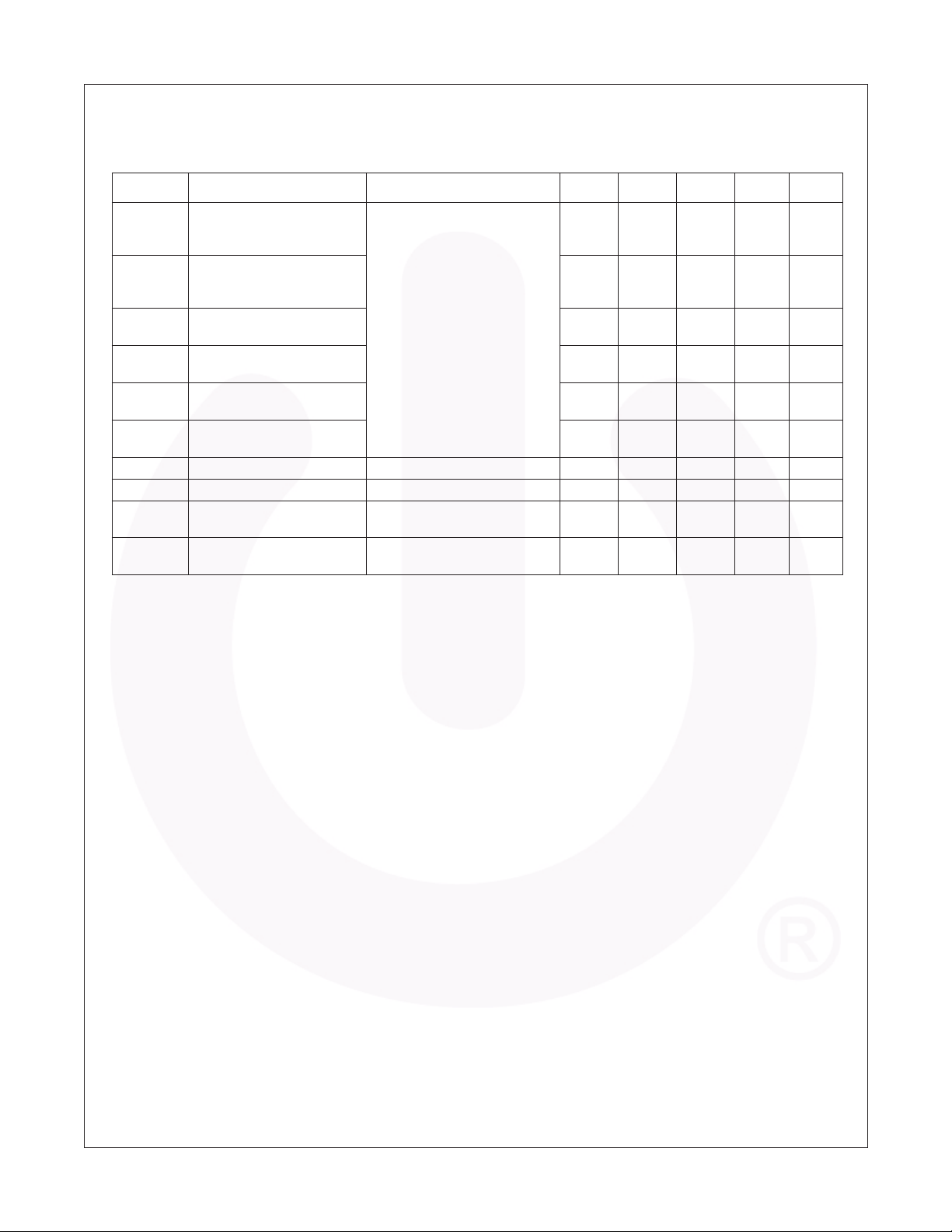
Switching Characteristics
Apply over all recommended conditions, typical value is measured at VDD = 30V, VSS = Ground, TA = 25°C unless
otherwise specified.
Symbol Parameter Conditions Min. Typ. Max. Units Figure
t
PHL
t
PLH
PWD Pulse Width Distortion
PDD
(Skew)
t
t
t
ULVO ON
t
ULVO OFF
|CMH| Common Mode Transient
|CML| Common Mode Transient
Propagation Delay Time to
Logic Low Output
Propagation Delay Time to
Logic High Output
|t
– t
PHL
PLH
Propagation Delay Difference
Between Any Two Parts
Output Rise Time
R
(10% to 90%)
Output Fall Time
F
(90% to 10%)
ULVO Turn On Delay IF = 10mA, VO > 5V 0.8 µs
ULVO Turn Off Delay IF = 10mA, VO < 5V 0.4 µs
Immunity at Output High
Immunity at Output Low
(9)
(10)
(11)
|
(12)
IF = 10mA to 16mA, Rg = 10Ω,
Cg =10nF, f = 10kHz,
Duty Cycle = 50%
TA = 25°C, VDD = 30V,
IF = 10 to 16mA, VCM = 2000V
TA = 25°C, VDD = 30V, VF = 0V,
VCM = 2000V
(14)
100 285 500 ns 10, 11,
100 260 500 ns 10, 11,
25 300 ns
-350 350
60 ns 27
60 ns 27
20 50 kV/µs 28
(13)
20 50 kV/µs 28
12, 13,
14, 27
12, 13,
14, 27
FOD8321 — 2.5A Output Current, Gate Drive Optocoupler in Optoplanar
Notes:
9. t
10. t
11. PWD is defined as | t
12. The difference between t
propagation delay is measured from the 50% level on the falling edge of the input pulse to the 50% level of the
PHL
falling edge of the V
propagation delay is measured from the 50% level on the rising edge of the input pulse to the 50% level of the
PLH
rising edge of the V
signal.
O
signal.
O
PHL
– t
| for any given device.
PLH
PHL
and t
between any two FOD8321 parts under same operating conditions, with equal
PLH
loads.
13. Common mode transient immunity at output high is the maximum tolerable negative dVcm/dt on the trailing edge of
the common mode impulse signal, Vcm, to assure that the output will remain high (i.e. V
> 15.0V).
O
14. Common mode transient immunity at output low is the maximum tolerable positive dVcm/dt on the leading edge of
the common pulse signal, Vcm, to assure that the output will remain low (i.e. V
< 1.0V).
O
®
Wide Body SOP 5-Pin
©2010 Fairchild Semiconductor Corporation www.fairchildsemi.com
FOD8321 Rev. 1.0.4 6
Page 7
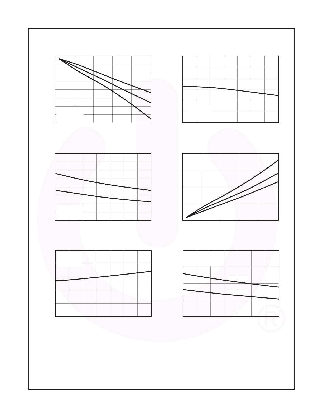
Typical Performance Characteristics
FOD8321 — 2.5A Output Current, Gate Drive Optocoupler in Optoplanar
Figure 1. Output High Voltage Drop vs. Output High Current
0
-0.5
-1.0
-1.5
-2.0
-2.5
-3.0
– OUTPUT HIGH VOLTAGE DROP (V)
VDD = 15V to 30V
DD
– V
OH
V
= 0V
V
SS
-3.5
I
= 10mA to 16mA
F
f = 200Hz 0.2% Duty Cycle
-4.0
0 0.5 1.0 1.5 2.0 2.5
= -40°C
T
A
25°C
100°C
IOH – OUTPUT HIGH CURRENT (A)
Figure 3. Output High Current vs. Ambient Temperature
8
7
6
5
4
3
2
– OUTPUT HIGH CURRENT (A)
VDD = 15V to 30V
OH
I
= 0V
V
SS
1
I
= 10mA to 16mA
F
f = 200Hz 0.2% Duty Cycle
0
-40 -20 0 20 40 60 80 100
TA – AMBIENT TEMPERATURE (°C)
VO = VDD – 6V
V
= VDD – 3V
O
Figure 2. Output High Voltage Drop vs. Ambient Temperature
0
-0.05
-0.10
-0.15
-0.20
VDD = 15V to 30V
– OUTPUT HIGH VOLTAGE DROP (V)
-0.25
V
DD
–V
OH
V
-0.30
= 0V
SS
= 10mA to 16mA
I
F
I
= -100mA
O
-40 -20 0 20 40 60 80 100
TA – AMBIENT TEMPERATURE (°C)
Figure 4. Output Low Voltage vs. Output Low Current
4
VDD = 15V to 30V
= 0V
V
SS
= 0mA
I
F
f = 200Hz 99.8% Duty Cycle
3
2
1
– OUTPUT LOW VOLTAGE (V)
OL
V
0
0 0.5 1.0 1.5 2.0 2.5
IOL – OUTPUT LOW CURRENT (A)
= 100°C
T
A
25°C
-40°C
Figure 5. Output Low Voltage vs. Ambient Temperature
0.25
VDD = 15V to 30V
= 0V
V
SS
V
= 0V or 0.8V
F
0.20
= 100mA
I
O
0.15
0.10
– OUTPUT LOW VOLTAGE (V)
0.05
OL
V
0
-40 -20 0 20 40 60 80 100
TA – AMBIENT TEMPERATURE (°C)
Figure 6. Output Low Current vs. Ambient Temperature
8
VDD = 15V to 30V
= 0V
V
SS
I
= 0A
F
f = 200Hz 99.8% Duty Cycle
6
4
2
– OUTPUT LOW CURRENT (A)
OL
I
0
-40 -20 0 20 40 60 80 100
TA – AMBIENT TEMPERATURE (°C)
VO = VSS + 6V
VO = VSS + 3V
®
Wide Body SOP 5-Pin
©2010 Fairchild Semiconductor Corporation www.fairchildsemi.com
FOD8321 Rev. 1.0.4 7
Page 8
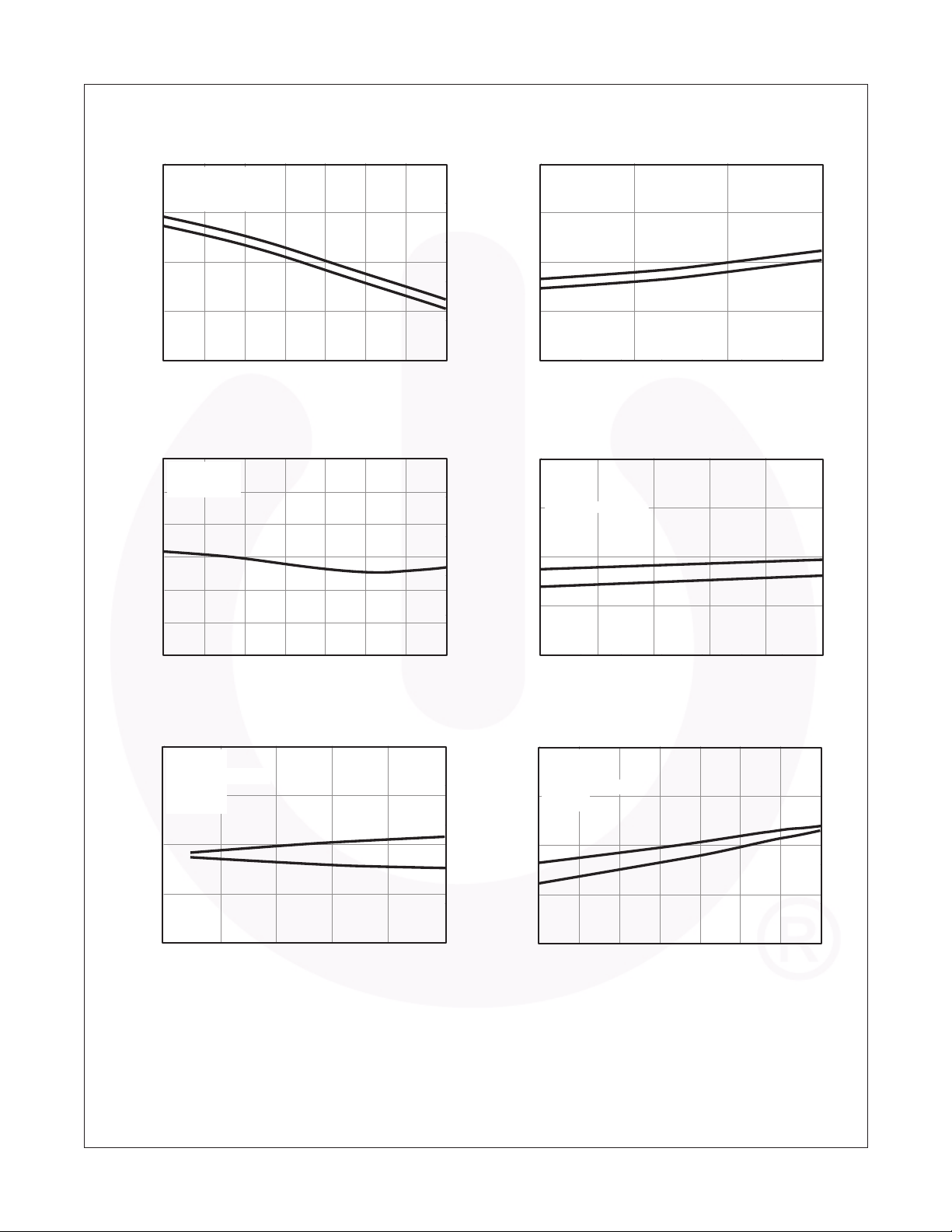
Typical Performance Characteristics (Continued)
FOD8321 — 2.5A Output Current, Gate Drive Optocoupler in Optoplanar
Figure 7. Supply Current vs. Ambient Temperature
3.6
VDD = 30V
V
= 0V
SS
I
= 10mA (for I
F
= 0mA (for I
I
F
3.2
2.8
2.4
– SUPPLY CURRENT (mA)
DD
I
2.0
-40 -20 0 20 40 60 80 100
DDL
DDH
)
)
I
DDH
I
DDL
TA – AMBIENT TEMPERATURE (°C)
Figure 9. Low to High Input Current Threshold
4
VDD = 15V to 30V
= 0V
V
SS
Output = Open
3.5
3.0
2.5
2.0
THRESHOLD (mA)
1.5
– LOW TO HIGH INPUT CURRENT
FLH
I
1.0
-40 -20 0 20 40 60 80 100
vs. Ambient Temperature
TA – AMBIENT TEMPERATURE (°C)
Figure 11. Propagation Delay vs. LED Forward Current
500
VDD = 30V
V
= 0V
SS
f = 10kHz 50% Duty Cycle
= 10Ω
R
g
400
C
= 10nF
g
= 25°C
T
A
t
t
PHL
PLH
300
200
– PROPAGATION DELAY (ns)
P
t
Figure 8. Supply Current vs. Supply Voltage
3.6
IF = 10mA (for I
I
= 0mA (for I
F
V
= 0V
SS
= 25°C
T
A
3.2
2.8
2.4
– SUPPLY CURRENT (mA)
DD
I
2.0
15 20 25 30
DDL
DDH
)
)
I
DDH
I
DDL
VDD – SUPPLY VOLTAGE (V)
Figure 10. Propagation Delay vs. Supply Voltage
500
IF = 10mA
= 10Ω
R
g
C
= 10nF
g
= 25°C
T
A
400
f = 10kHz 50% Duty Cycle
t
300
200
– PROPAGATION DELAY (ns)
P
t
100
15 18 21 24 27 30
PHL
t
PLH
VDD – SUPPLY VOLTAGE (V)
Figure 12. Propagation Delay vs. Ambient Temperature
500
VDD = 30V
V
= 0V
SS
I
= 10mA
F
f = 10kHz 50% Duty Cycle
400
Rg = 10Ω
= 10nF
C
g
t
t
PHL
PLH
300
200
– PROPAGATION DELAY (ns)
P
t
®
Wide Body SOP 5-Pin
100
6 8 10 12 14 16
IF – FORWARD LED CURRENT (mA)
100
-40 -20 0 20 40 60 80 100
TA – AMBIENT TEMPERATURE (°C)
©2010 Fairchild Semiconductor Corporation www.fairchildsemi.com
FOD8321 Rev. 1.0.4 8
Page 9
Typical Performance Characteristics (Continued)
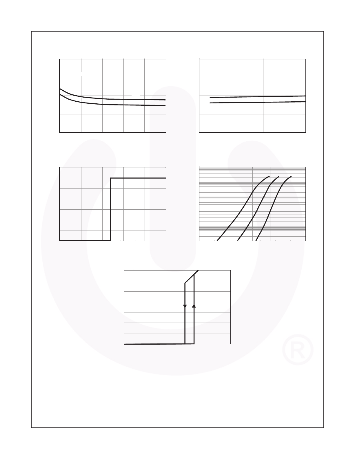
Figure 13. Propagation Delay vs. Series Load Resistance
500
VDD = 30V
V
= 0V
SS
= 10mA
I
F
f = 10kHz 50% Duty Cycle
400
C
= 10nF
g
= 25°C
T
A
t
t
PHL
PLH
300
200
– PROPAGATION DELAY (ns)
P
t
Figure 14. Propagation Delay vs. Load Capacitance
500
VDD = 30V
V
= 0V
SS
= 10mA
I
F
f = 10kHz 50% Duty Cycle
400
R
= 10Ω
g
= 25°C
T
A
300
200
– PROPAGATION DELAY (ns)
P
t
t
t
PHL
PLH
FOD8321 — 2.5A Output Current, Gate Drive Optocoupler in Optoplanar
100
0 1020304050
Rg – SERIES LOAD RESISTANCE (Ω)
Figure 15. Transfer Characteristics
35
VDD = 30V
T
= 25°C
A
30
25
20
15
10
– OUTPUT VOLTAGE (V)
O
V
5
0
012345
IF – FORWARD LED CURRENT (mA)
Figure 17. Under Voltage Lockout
14
IF = 10mA
= 25°C
T
A
12
10
100
0 20406080100
Cg – LOAD CAPACITANCE (nF)
Figure 16. Input Forward Current vs. Forward Voltage
100
10
100°C
1
0.1
– FORWARD CURRENT (mA)
0.01
F
I
0.001
0.6 0.8 1.0 1.2 1.4 1.6 1.8
25°C
VF – FORWARD VOLTAGE (V)
-40°C
®
Wide Body SOP 5-Pin
8
6
4
– OUTPUT VOLTAGE (V)
O
V
2
0
0 5 10 15 20
V
= 11.56V V
UVLO
UVLO
= 13.12V
VDD–VSS – SUPPLY VOLTAGE (V)
©2010 Fairchild Semiconductor Corporation www.fairchildsemi.com
FOD8321 Rev. 1.0.4 9
Page 10
Test Circuit
Pulse Generator
PW = 4.99ms
Period = 5ms
R
= 50Ω
OUT
LED-IFmon
Test Conditions:
Frequency = 200Hz
Duty Cycle = 99.8%
= 15V to 30V
V
DD
V
= 0V
SS
I
= 0mA
F
Pulse-In
R2
100Ω
R1
100Ω
FOD8321 — 2.5A Output Current, Gate Drive Optocoupler in Optoplanar
Power Supply
+
+
C1
0.1μF
1
3
6
5
V
OL
4
I
OL
D1
C2
47μF
C3
0.1μF
+
C4
47μF
To Scope
VDD = 15V to 30V
Power Supply
+
V = 6V
Pulse Generator
PW = 10μs
Period = 5ms
R
= 50Ω
OUT
LED-IFmon
Test Conditions:
Frequency = 200Hz
Duty Cycle = 0.2%
= 15V to 30V
V
DD
V
= 0V
SS
I
= 10mA to 16mA
F
Pulse-In
R2
100Ω
R1
100Ω
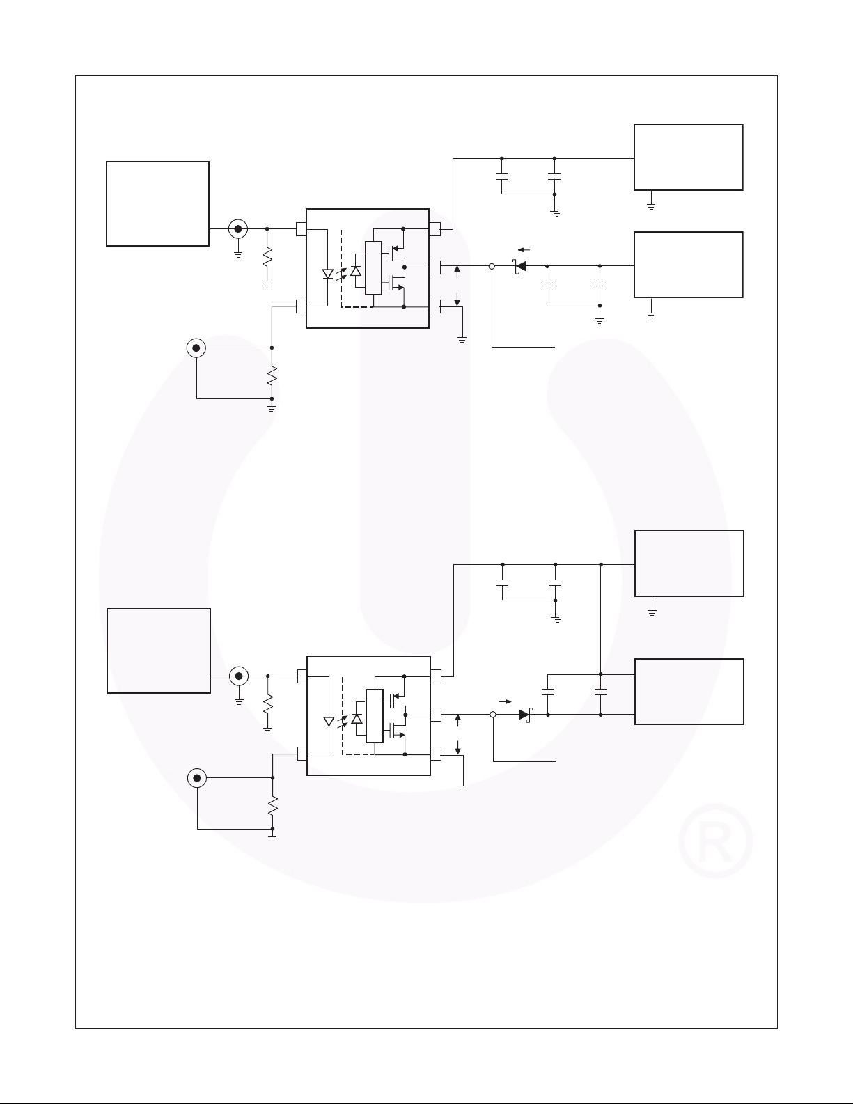
Figure 18. I
Test Circuit
OL
Power Supply
+
+
C1
0.1μF
1
3
6
I
OH
5
V
OH
4
Current
Probe
D1
C2
47μF
C3
0.1μF
To Scope
+
C4
47μF
VDD = 15V to 30V
+
Power Supply
V = 6V
–
®
Wide Body SOP 5-Pin
Figure 19. I
©2010 Fairchild Semiconductor Corporation www.fairchildsemi.com
FOD8321 Rev. 1.0.4 10
Test Circuit
OH
Page 11
Test Circuit (Continued)
FOD8321 — 2.5A Output Current, Gate Drive Optocoupler in Optoplanar
IF = 10 to 16mA
1
3
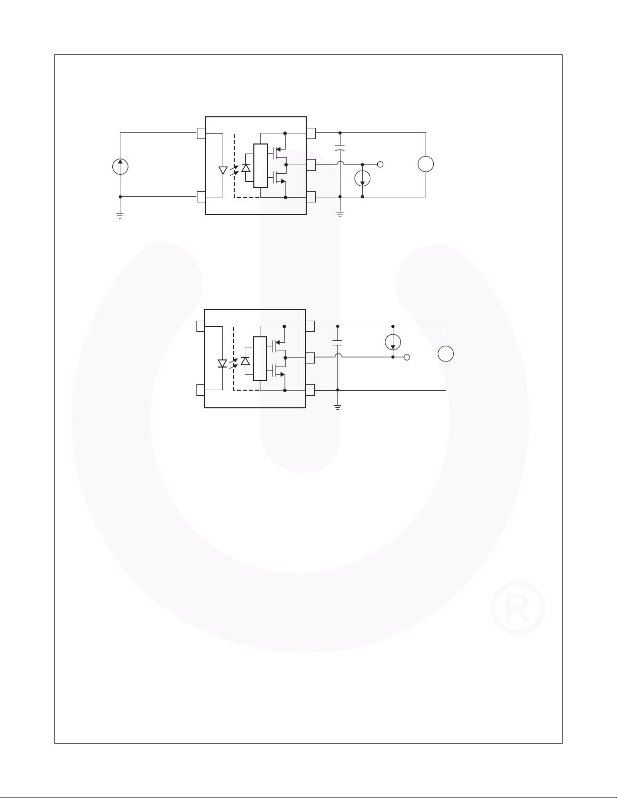
Figure 20. V
1
3
6
5
4
Test Circuit
OH
6
5
4
0.1μF
0.1μF
V
100mA
O
100mA
VO
+
VDD = 15 to 30V
–
+
VDD = 15 to 30V
–
Figure 21. V
Test Circuit
OL
®
Wide Body SOP 5-Pin
©2010 Fairchild Semiconductor Corporation www.fairchildsemi.com
FOD8321 Rev. 1.0.4 11
Page 12
Test Circuit (Continued)
FOD8321 — 2.5A Output Current, Gate Drive Optocoupler in Optoplanar
IF = 10 to 16mA
+
VF = -3.0 to 0.8V
–
1
3
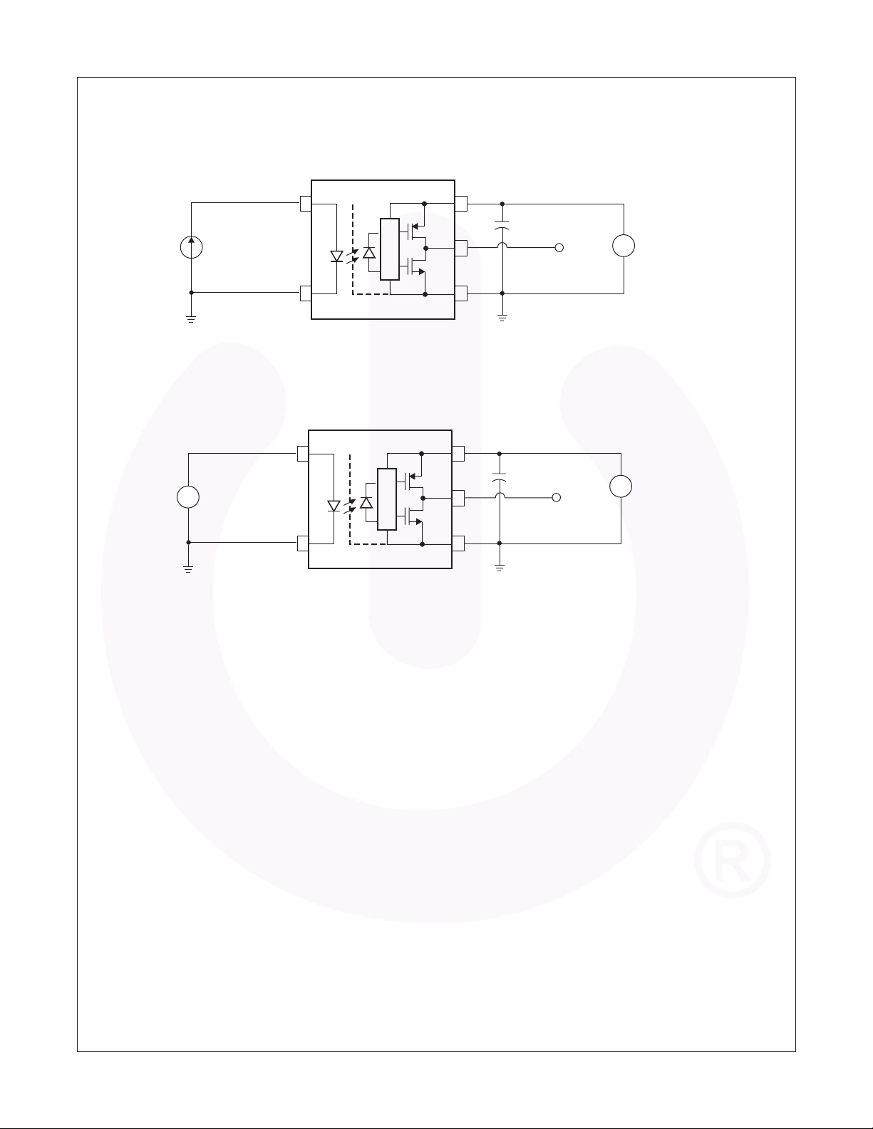
Figure 22. I
1
3
Figure 23. I
6
5
4
Test Circuit
DDH
6
5
4
Test Circuit
DDL
0.1μF
0.1μF
+
V
O
V
O
VDD = 30V
–
+
VDD = 30V
–
®
Wide Body SOP 5-Pin
©2010 Fairchild Semiconductor Corporation www.fairchildsemi.com
FOD8321 Rev. 1.0.4 12
Page 13
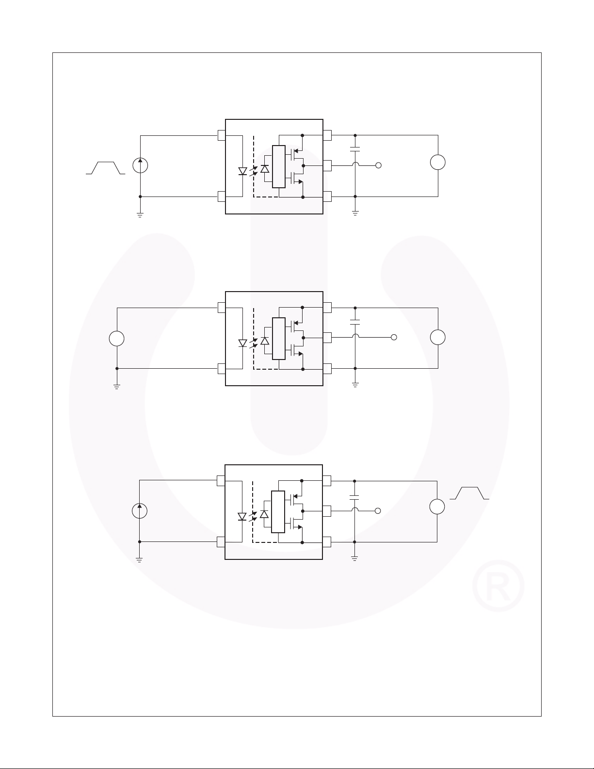
Test Circuit (Continued)
FOD8321 — 2.5A Output Current, Gate Drive Optocoupler in Optoplanar
IF
+
VF = –3.0 to 0.8V
–
1
3
1
3
Figure 24. I
Figure 25. V
Test Circuit
FLH
Test Circuit
FHL
6
0.1μF
0.1μF
VO > 5V
V
O
5
4
6
5
4
+
VDD = 15 to 30V
–
+
VDD = 15 to 30V
–
IF = 10mA
1
3
Figure 26. UVLO Test Circuit
®
Wide Body SOP 5-Pin
6
0.1μF
5
4
VO = 5V
+
–
15V or 30V
Ramp
V
DD
©2010 Fairchild Semiconductor Corporation www.fairchildsemi.com
FOD8321 Rev. 1.0.4 13
Page 14
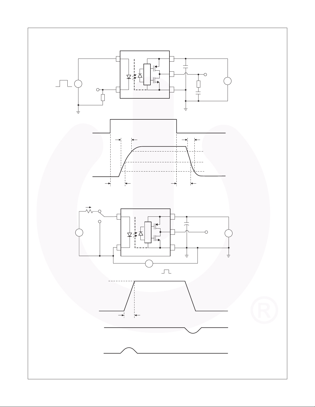
Test Circuit (Continued)
FOD8321 — 2.5A Output Current, Gate Drive Optocoupler in Optoplanar
f = 10KHz
DC = 50%
5V
1
+
–
Probe
I
F
50Ω
3
t
R
6
0.1μF
5
4
t
F
VO
Rg = 10Ω
Cg = 10nF
+
VDD = 15 to 30V
–
90%
50%
+
–
V
OUT
Figure 27. t
I
F
t
PLH
, t
PHL
A
1
B
, tR and tF Test Circuit and Waveforms
PLH
t
PHL
6
5
0.1μF
10%
V
+
O
VDD = 30V
–
®
Wide Body SOP 5-Pin
3
+ –
= 2,000V
V
CM
V
CM
4
0V
Δt
V
O
V
OH
Switch at A: IF = 10mA
V
O
Switch at B: I
= 0mA
F
V
OL
Figure 28. CMR Test Circuit and Waveforms
©2010 Fairchild Semiconductor Corporation www.fairchildsemi.com
FOD8321 Rev. 1.0.4 14
Page 15
Ordering Information
Part Number Package Packing Method
FOD8321 Wide Body SOP 5-Pin Tube (100 units per tube)
FOD8321R2 Wide Body SOP 5-Pin Tape and Reel (1,000 units per reel)
FOD8321V Wide Body SOP 5-Pin, DIN EN/IEC60747-5-5 Option Tube (100 units per tube)
FOD8321R2V Wide Body SOP 5-Pin, DIN EN/ IEC60747-5-5 Option Tape and Reel (1,000 units per reel)
All packages are lead free per JEDEC: J-STD-020B standard.
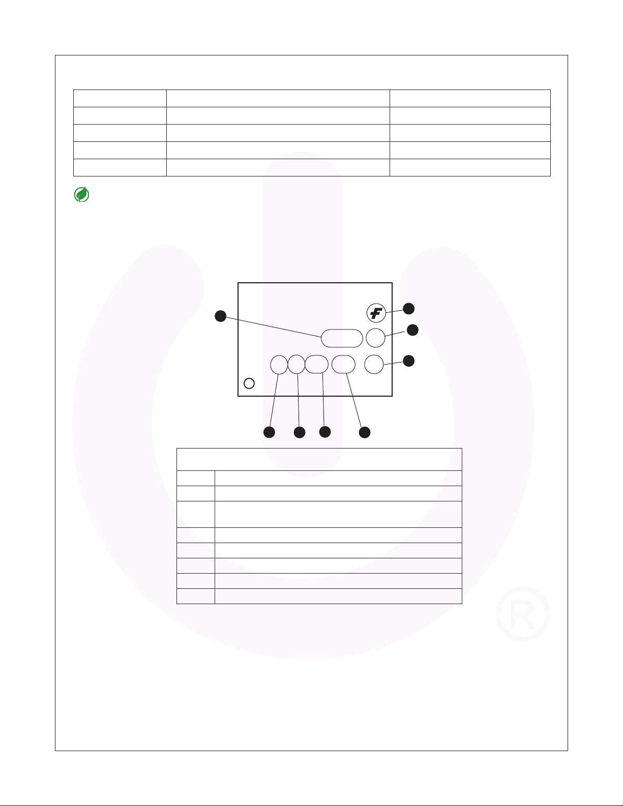
Marking Information
FOD8321 — 2.5A Output Current, Gate Drive Optocoupler in Optoplanar
2
8321
D X YY KK
4
6
5
V
W
7
Definitions
1 Fairchild logo
2 Device number, e.g., ‘8321’ for FOD8321
3 DIN EN/IEC60747-5-5 Option (only appears on
component ordered with this option)
4 Plant code, e.g., ‘D’
5 Last digit year code, e.g., ‘C’ for 2012
6 Two digit work week ranging from ‘01’ to ‘53’
7 Lot traceability code
8 Package assembly code, W
1
3
8
®
Wide Body SOP 5-Pin
©2010 Fairchild Semiconductor Corporation www.fairchildsemi.com
FOD8321 Rev. 1.0.4 15
Page 16
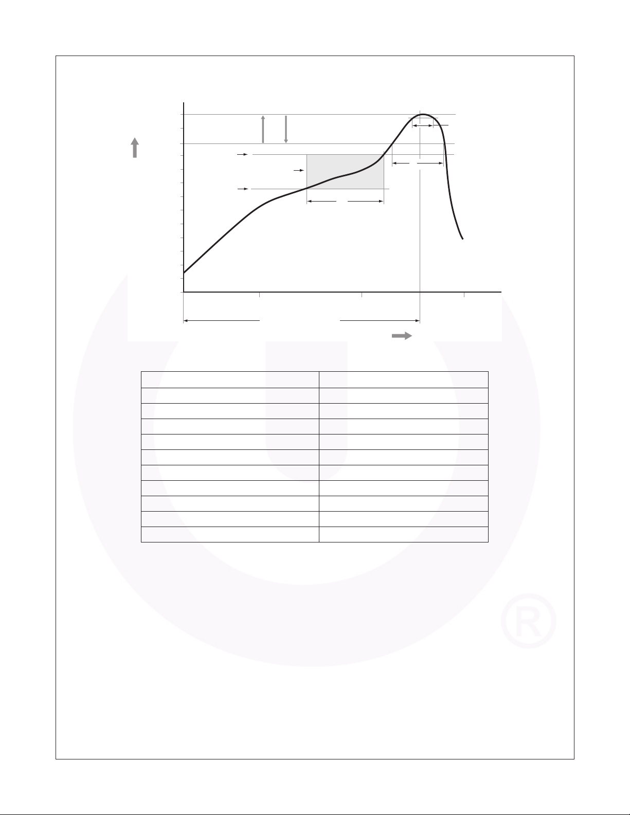
Reflow Profile
FOD8321 — 2.5A Output Current, Gate Drive Optocoupler in Optoplanar
Max. Ramp-up Rate = 3°C/S
Max. Ramp-down Rate = 6°C/S
Ts ma x
Preheat Area
Ts mi n
t
L
t
s
260
240
220
200
180
160
140
120
T
P
T
L
100
80
60
Temperature (°C)
40
20
0
120
240 360
Time 25°C to Peak
Time (seconds)
Profile Freature Pb-Free Assembly Profile
Temperature Min. (Tsmin) 150°C
Temperature Max. (Tsmax) 200°C
Time (t
Ramp-up Rate (t
Liquidous Temperature (T
Time (t
Peak Body Package Temperature 260°C +0°C / –5°C
Time (t
Ramp-down Rate (T
Time 25°C to Peak Temperature 8 minutes max.
) from (Tsmin to Tsmax) 60–120 seconds
S
to tP) 3°C/second max.
L
) 217°C
L
) Maintained Above (TL) 60–150 seconds
L
) within 5°C of 260°C 30 seconds
P
to TL) 6°C/second max.
P
t
P
®
Wide Body SOP 5-Pin
©2010 Fairchild Semiconductor Corporation www.fairchildsemi.com
FOD8321 Rev. 1.0.4 16
Page 17
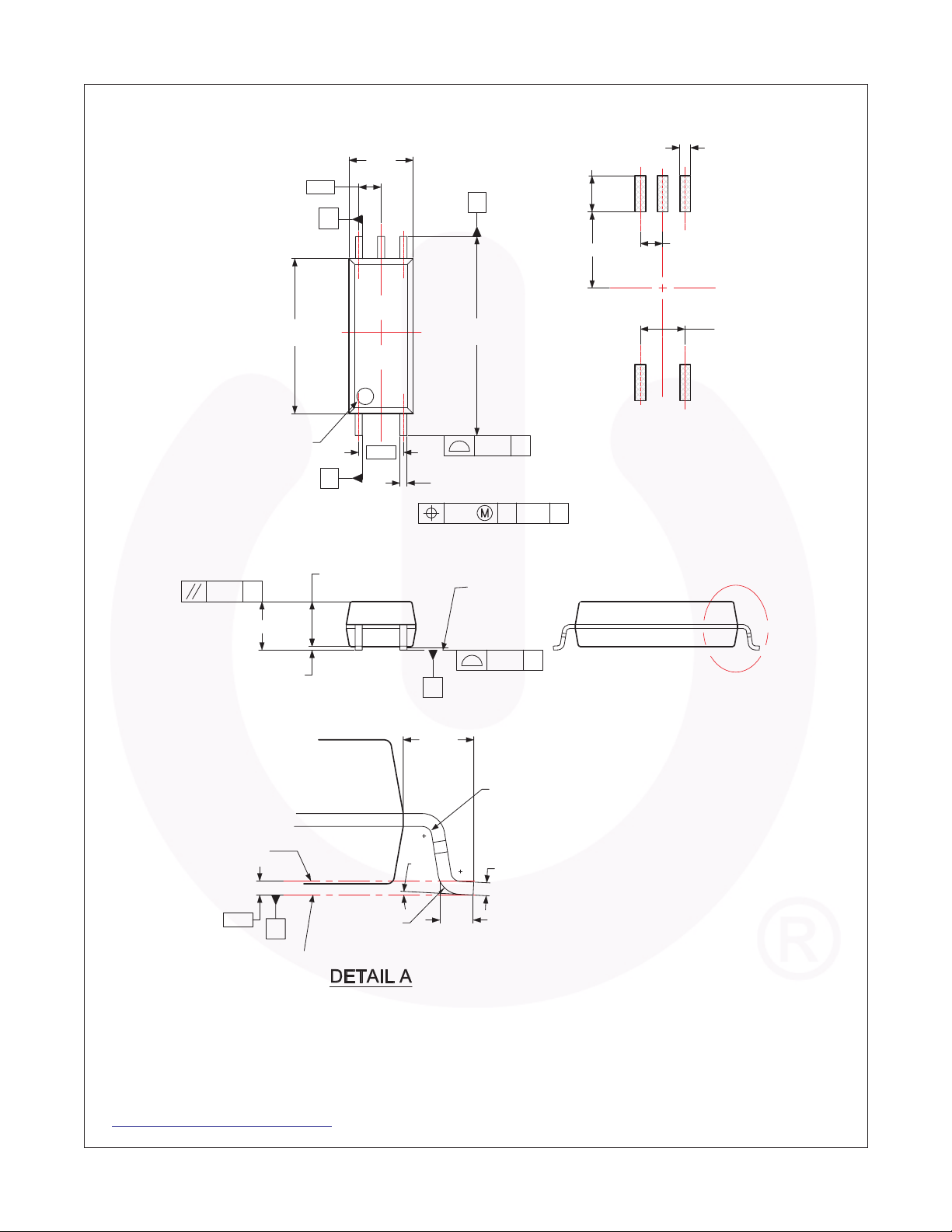
Package Dimensions
FOD8321 — 2.5A Output Current, Gate Drive Optocoupler in Optoplanar
INDICATOR
0.10 C
2.95 MAX
9.30
8.30
PIN ONE
1.27
A
6
B
2.65
2.45
4.15
3.15
2.05
6
0.60
4
D
4
4.33
11.80
10.80
LAND PATTERN
RECOMMENDATION
2.54
3
0.33
C
5 TIPS
0.51
5X
0.31
1
1.27
2.54
1
3
0.25 C A-B D
A
SEATING
PLANE
0.10
C
NOTES: UNLESS OTHERWISE SPECIFIED
A) THIS PACKAGE DOES NOT
(R0.54
0.25
0.19
CONFORM TO ANY STANDARD.
B) ALL DIMENSIONS ARE IN
)
MILLIMETERS.
C) DIMENSIONS ARE EXCLUSIVE OF
BURRS, MOLD FLASH AND TIE BAR
PROTRUSIONS
D) DRAWING CONFORMS TO ASME
Y14.5M-1994
E) DRAWING FILE NAME:
MKT-M05BREV1
GAUGE
PLANE
0.25
0.30
0.10
C
(R1.29)
C
(1.25)
8°
0°
5X
1.04
0.44
SEATING PLANE
SCALE: 3.2:1
Package drawings are provided as a service to customers considering Fairchild components. Drawings may change in any manner
without notice. Please note the revision and/or date on the drawing and contact a Fairchild Semiconductor representative to verify or
obtain the most recent revision. Package specifications do not expand the terms of Fairchild’s worldwide terms and conditions,
specifically the warranty therein, which covers Fairchild products.
Always visit Fairchild Semiconductor’s online packaging area for the most recent package drawings:
http://www.fairchildsemi.com/packaging/
®
Wide Body SOP 5-Pin
©2010 Fairchild Semiconductor Corporation www.fairchildsemi.com
FOD8321 Rev. 1.0.4 17
Page 18
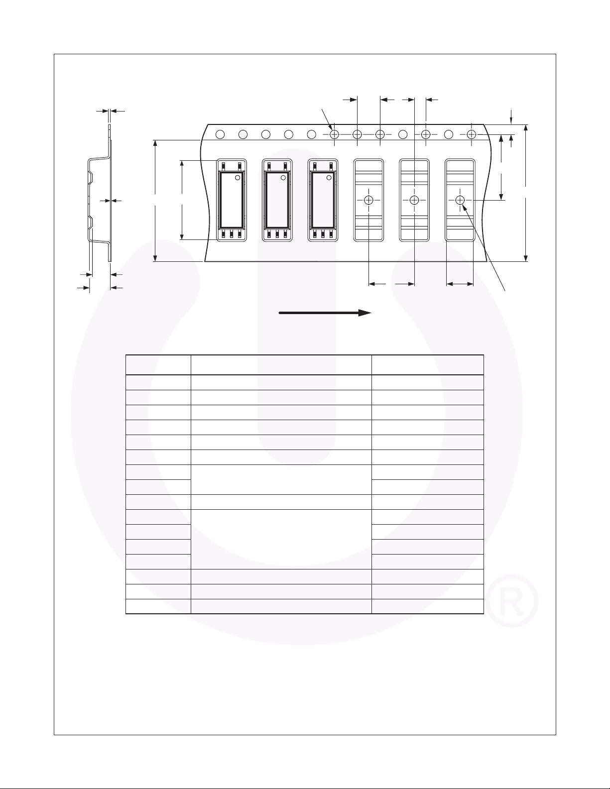
Carrier Tape Specification (SOIC-5L OPTO R2 & R2V Option)
FOD8321 — 2.5A Output Current, Gate Drive Optocoupler in Optoplanar
K1
Ko
t
W1
d
Bo
Do
Po
P
User Direction of Feed
Symbol Description Dimmension in mm
W Tape Width 24.00 + 0.20 / -0.10
t Tape Thickness 0.30 ± 0.05
Po Sprocket Hole Pitch 4.00 ± 0.20
Do Sprocket Hole Diameter 1.50 + 0.10 / -0.00
D1 Pocket Hole Diameter 1.50 + 0.25 / -0.00
E Sprocket Hole Location 1.75 ± 0.10
F Pocket Location 11.50 ± 0.10
P2 2.00 ± 0.10
P Pocket Pitch 8.00 ± 0.10
Ao Pocket Dimension 4.50 ± 0.10
Bo 12.00 ± 0.10
Ko 3.35 ± 0.10
K1 2.85 ± 0.10
W1 Cover Tape Width 21.30 ± 0.10
d Cover Tape Thickness 0.05 ± 0.01
Max Component Rotation or Tilt 10°
P2
Ao
E
F
W
D1
®
Wide Body SOP 5-Pin
©2010 Fairchild Semiconductor Corporation www.fairchildsemi.com
FOD8321 Rev. 1.0.4 18
Page 19
FOD8321 — 2.5A Output Current, Gate Drive Optocoupler in Optoplanar
®
Wide Body SOP 5-Pin
©2010 Fairchild Semiconductor Corporation www.fairchildsemi.com
FOD8321 Rev. 1.0.4 19
 Loading...