

Page 1
tm
FOD814 Series, FOD617 Series, FOD817 Series 4-Pin High Operating Temperature Phototransistor Optocouplers
May 2006
FOD814 Series, FOD617 Series, FOD817 Series
4-Pin High Operating Temperature
Phototransistor Optocouplers
Features
AC input response (FOD814 only)
■
■
Applicable to Pb-free IR reflow soldering
Compact 4-pin package
■
■
Current transfer ratio in selected groups:
FOD617A: 40–80% FOD817: 50–600%
FOD617B: 63–125% FOD817A:80–160%
FOD617C:100–200% FOD817B: 130–260%
FOD617D:160–320% FOD817C:200–400%
FOD814: 20–300% FOD817D:300–600%
FOD814A: 50–150%
C-UL, UL and VDE approved
■
■
High input-output isolation voltage of 5000Vrms
Minimum BV
■
■
Higher operating temperatures (versus H11AXXX
of 70V guaranteed
CEO
counterparts)
Applications
FOD814 Series
AC line monitor
■
■
Unknown polarity DC sensor
Telephone line interface
■
FOD617 and FOD817 Series
Power supply regulators
■
■
Digital logic inputs
Microprocessor inputs
■
Description
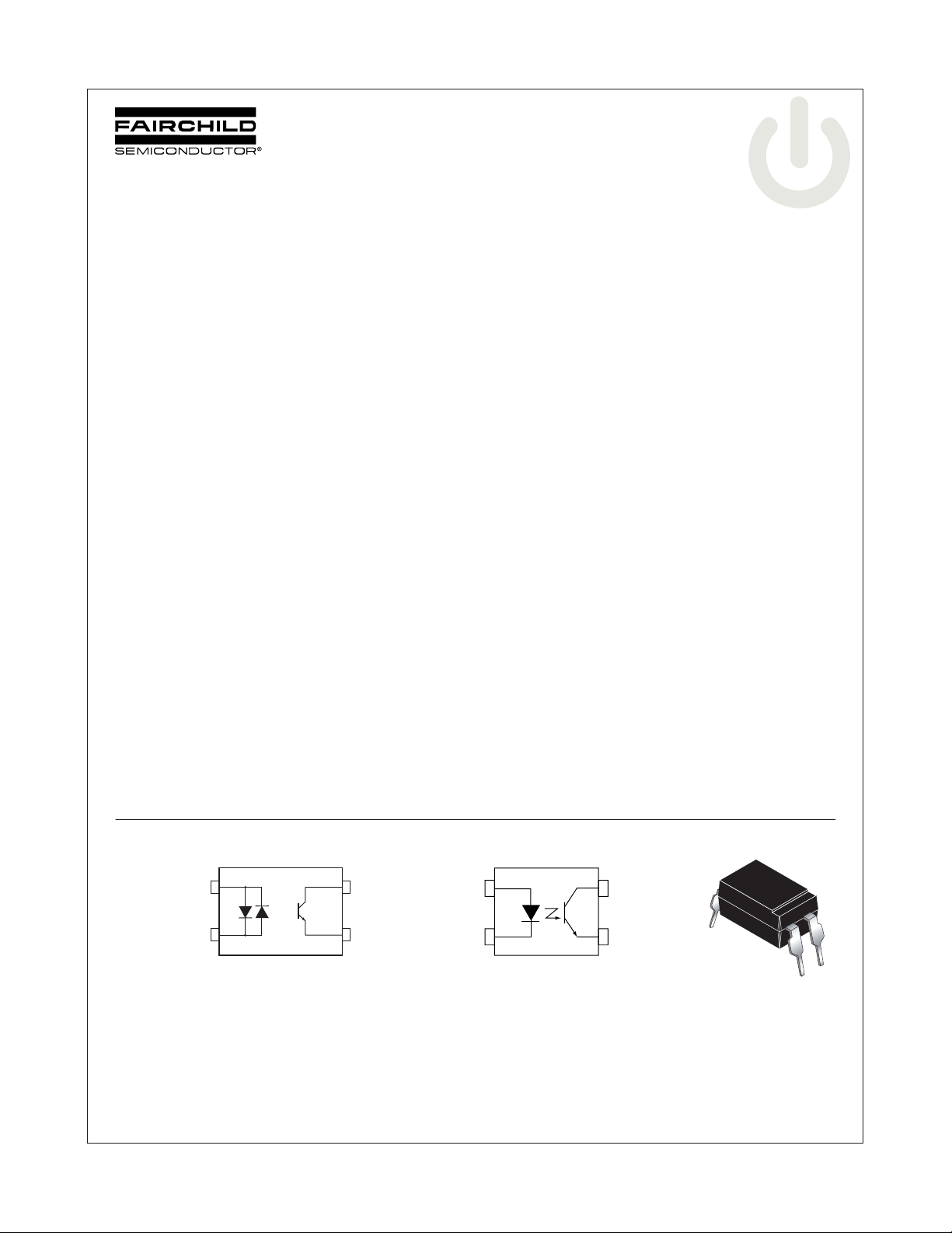
The FOD814 consists of two gallium arsenide infrared
emitting diodes, connected in inverse parallel, driving a
silicon phototransistor output in a 4-pin dual in-line
package. The FOD617/817 Series consists of a gallium
arsenide infrared emitting diode driving a silicon
phototransistor in a 4-pin dual in-line package.
Functional Block Diagram
1ANODE, CATHODE
2
FOD814 FOD617/817
©2006 Fairchild Semiconductor Corporation
FOD814 Series, FOD617 Series, FOD817 Series Rev. 1.0.5
4
COLLECTOR
3CATHODE, ANODE
EMITTER
CATHODE
1
2
1
4
COLLECTORANODE
3 EMITTER
4
1
www.fairchildsemi.com
Page 2
FOD814 Series, FOD617 Series, FOD817 Series 4-Pin High Operating Temperature Phototransistor Optocouplers
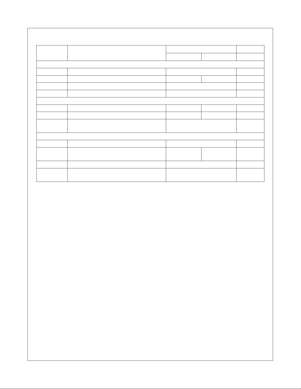
Absolute Maximum Ratings
Symbol Parameter
TOTAL DEVICE
T
STG
T
OPR
T
SOL
P
TOT
EMITTER
I
F
V
R
P
D
DETECTOR
V
CEO
V
ECO
I
C
P
C
Storage Temperature -55 to +150 °C
Operating Temperature -55 to +105 -55 to +110 °C
Lead Solder Temperature 260 for 10 sec °C
Total Power Dissipation 200 mW
Continuous Forward Current ±50 50 mA
Reverse Voltage – 6
Power Dissipation
Derate above 100°C
Collector-Emitter Voltage 70 V
Emitter-Collector Voltage 6 6 (FOD817)
Continuous Collector Current 50 mA
Collector Power Dissipation
Derate above 90°C
(T
= 25°C Unless otherwise specified.)
A
FOD814 FOD617/817
Value Units
70
1.7
7 (FOD617)
150
2.9
mW
mW/°C
V
mW
mW/°C
FOD814 Series, FOD617 Series, FOD817 Series Rev. 1.0.5
2
www.fairchildsemi.com
Page 3
FOD814 Series, FOD617 Series, FOD817 Series 4-Pin High Operating Temperature Phototransistor Optocouplers
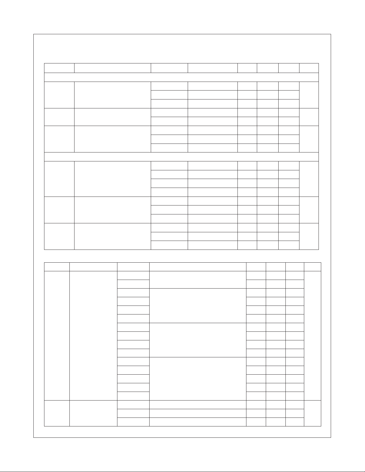
Electrical Characteristics
(T
= 25°C Unless otherwise specified.)
A
Individual Component Characteristics
Symbol Parameter Device Test Conditions Min. Typ.* Max. Unit
EMITTER
V
I
C
DETECTOR
I
CEO
BV
BV
Forward Voltage FOD814 I
F
FOD617 I
FOD817 I
Reverse Leakage Current FOD617 V
R
FOD817 V
Te r minal Capacitance FOD814 V = 0, f = 1kHz – 50 250 pF
t
= ±20mA – 1.2 1.4 V
F
= 60mA – 1.35 1.65
F
= 20mA – 1.2 1.4
F
= 6.0V – 0.001 10 µA
R
= 4.0V – – 10
R
FOD617 V = 0, f = 1kHz – 30 250
FOD817 V = 0, f = 1kHz – 30 250
Collector Dark Current FOD814 V
Collector-Emitter Breakdown
CEO
Voltage
Emitter-Collector Breakdown
ECO
Voltage
FOD617C/D V
FOD617A/B V
FOD817 V
FOD814 I
FOD617 I
FOD817 I
FOD814 I
FOD617 I
FOD817 I
= 20V, I
CE
= 10V, I
CE
= 10V, I
CE
= 20V, I
CE
= 0.1mA, I
C
= 100µA, I
C
= 0.1mA, I
C
= 10µA, I
E
= 10µA, I
E
= 10µA, I
E
= 0 – – 100 nA
F
= 0 – 1 100
F
= 0 – 1 50
F
= 0 – – 100
F
= 0 70 – – V
F
= 0 70 – –
F
= 0 70 – –
F
= 0 6 – – V
F
= 0 7 – –
F
= 0 6 – –
F
Transfer Characteristics (T
= 25°C Unless otherwise specified.)
A
Symbol DC Characteristic Device Test Conditions Min. Typ.* Max. Unit
CTR Current Transfer
Ratio
FOD814 I
= ±1mA, V
F
CE
FOD814A 50 – 150
FOD617A I
= 10mA, V
F
CE
= 5V
= 5V
(1)
(1)
20 – 300 %
40 – 80
FOD617B 63 – 125
FOD617C 100 – 200
FOD617D 160 – 320
FOD617A I
= 1mA, V
F
CE
= 5V
(1)
13 – –
FOD617B 22 – –
FOD617C 34 – –
FOD617D 56 – –
FOD817 I
= 5mA, V
F
CE
= 5V
(1)
50 – 600
FOD817A 80 – 160
FOD817B 130 – 260
FOD817C 200 – 400
FOD817D 300 – 600
V
CE (sat)
*Typical values at T
Collector-Emitter
Saturation Voltage
= 25°C
A
FOD814 I
FOD617 I
FOD817 I
= ±20mA, I
F
= 10mA, I
F
= 20mA, I
F
= 1mA – 0.1 0.2 V
C
= 2.5mA – – 0.4
C
= 1mA – 0.1 0.2
C
FOD814 Series, FOD617 Series, FOD817 Series Rev. 1.0.5
3
www.fairchildsemi.com
Page 4

≤
—
FOD814 Series, FOD617 Series, FOD817 Series 4-Pin High Operating Temperature Phototransistor Optocouplers
Transfer Characteristics
(Continued) (T
= 25°C Unless otherwise specified.)
A
Symbol AC Characteristic Device Test Conditions Min. Typ.* Max. Unit
f
Cut-Off Frequency FOD814 V
C
= 5V, I
CE
= 2mA, R
C
= 100 Ω ,
L
15 80 – kHz
-3dB
t
Response Time (Rise) FOD814 V
r
= 2 V, I
CE
= 2mA, R
C
= 100 Ω
L
(2)
–418µs
FOD617
FOD817
Response Time (Fall) FOD814 – 3 18 µs
t
f
FOD617
FOD817
Isolation Characteristics
Symbol Characteristic Device Test Conditions Min. Typ.* Max. Units
V
R
C
Input-Output Isolation
ISO
ISO
ISO
(3)
Voltage
Isolation Resistance FOD814 V
Isolation Capacitance FOD814 V
FOD814 f = 60Hz, t = 1 min,
I
2µA
FOD617
I-O
FOD817
= 500VDC 5x10
I-O
FOD617
FOD817
= 0, f = 1 MHz 0.6 1.0 pf
I-O
FOD617
FOD817
5000 Vac(rms)
10
1x10
11
Ω
*Typical values at T
= 25°C
A
Notes:
1. Current Transfer Ratio (CTR) = I
/I
C
F
x 100%.
2. For test circuit setup and waveforms, refer to page 4.
3. For this test, Pins 1 and 2 are common, and Pins 3 and 4 are common.
FOD814 Series, FOD617 Series, FOD817 Series Rev. 1.0.5
4
www.fairchildsemi.com
Page 5
FOD814 Series, FOD617 Series, FOD817 Series 4-Pin High Operating Temperature Phototransistor Optocouplers
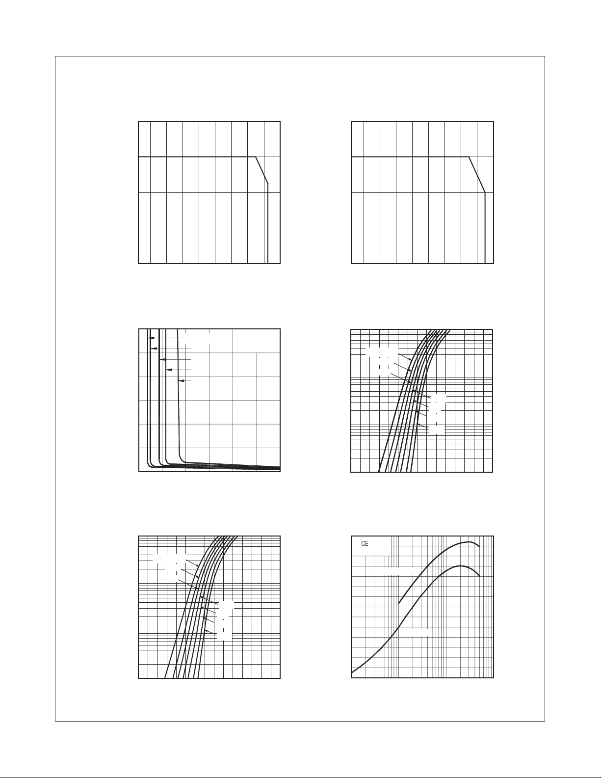
Typical Electrical/Optical Characteristics (T
Fig. 1 Collector Power Dissipation
vs. Ambient Temperature (FOD814)
200
(mW)
C
150
100
50
0
COLLECTOR POWER DISSIPATION P
-55
-40 -20 0 20 40 60 80 100 120
AMBIENT TEMPERATURE T
Fig. 3 Collector-Emitter Saturation Voltage
6
vs. Forward Current
Ic = 0.5 mA
5
4
(sat) (V)
CE
3
1m A
3m A
5m A
7m A
2
VOLTAGE V
1
COLLECTOR-EMITTER SATURATION
0
FORWARD CURRENT IF (mA)
(°C)
A
Ta = 25 °C
15.012.510.07.55.02.50
= 25°C Unless otherwise specified.)
A
Fig. 2 Collector Power Dissipation
vs. Ambient Temperature (FOD617/817)
200
(mW)
C
150
100
50
0
COLLECTOR POWER DISSIPATION P
-55
-40 -20 0 20 40 60 80 100 120
AMBIENT TEMPERATURE TA (°C)
Fig. 4 Forward Current vs. Forward Voltage
100
(mA)
F
10
TA = 105oC
1
(FOD814)
o
75
C
o
50
C
25
o
0
-30
-55oC
FORWARD CURRENT I
0.1
0.5 1.0 1.5 2.0
FORWARD VOLTAGE VF (V)
o
C
C
o
C
Fig. 5 Forward Current vs. Forward Voltage
(FOD617/817)
TA = 110oC
o
75
C
o
50
C
o
25
C
o
0
C
o
-30
C
-55oC
100
(mA)
F
10
1
FORWARD CURRENT I
0.1
0.5 1.0 1.5 2.0
FORWARD VOLTAGE VF (V)
FOD814 Series, FOD617 Series, FOD817 Series Rev. 1.0.5
Fig. 6 Current Transfer Ratio
140
120
100
V = 5V
Ta= 25°C
vs. Forward Current
FOD617/817
80
60
40
FOD814
20
CURRENT TRANSFER RATIO CTR ( %)
0
0.1 0 .2 0.5 1 2 5 10 20 50 100
FORWARD CURRENT IF (mA)
5 www.fairchildsemi.com
Page 6
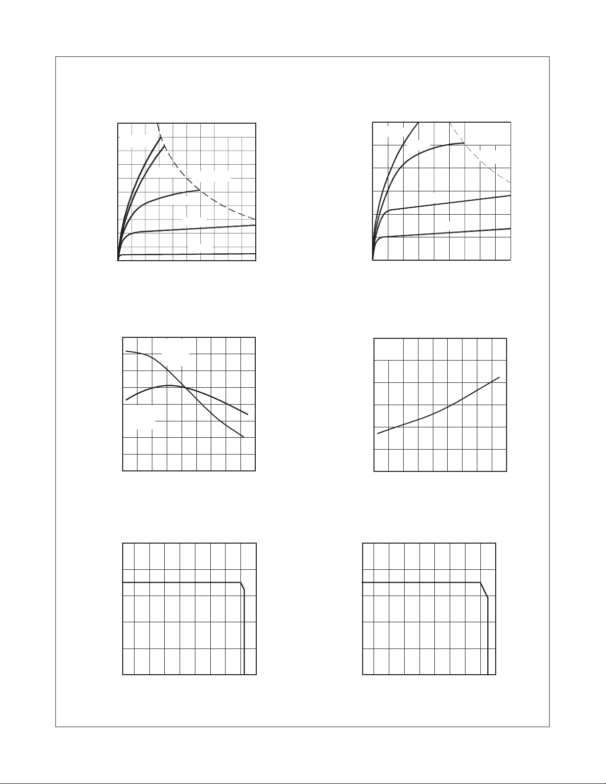
FOD814 Series, FOD617 Series, FOD817 Series 4-Pin High Operating Temperature Phototransistor Optocouplers
Typical Electrical/Optical Characteristics (Continued) (T
Fig. 7 Collector Current
vs. Collector-Emitter Voltage (FOD814)
50
I = 30 m A
F
40
(mA)
C
30
20
20 m A
10m A
5m A
10
COLLECTOR CURRENT I
0
0102030405060708090100
COLLECTOR-EMITTER VOLTAGE VCE (V)
Fig. 9 Relative Current Transfer Ratio
160
140
vs. Ambient Temperature
FOD814
IF = 1 mA
V
= 5V
CE
120
100
80
FOD617/817
IF = 5mA
60
RATIO (%)
= 5V
V
CE
40
20
RELATIVE CURRENT TRANSFER
0
-60 -40 -20 0 20 40 60 80 100 120
AMBIENT TEMPERATURE TA (°C)
Ta= 25°C
Pc(M AX.)
1m A
(sat) (V)
CE
VOLTAGE V
COLLECTOR-EMITTER SATURATION
= 25°C Unless otherwise specified.)
A
Fig. 8 Collector Current vs.
Collector-Emitter Voltage (FOD617/817)
30
I I
25
(mA)
C
= 30mA
F
20mA
Ta = 25°C
Pc(MAX.)
20
15
10mA
10
5m A
COLLECTOR CURRENT I
5
0
0102030405060708090
COLLECTOR-EMITTER VOLTAGE VCE (V)
Fig. 10 Collector-Emitter Saturation Voltage
vs. Ambient Temperature
0.12
IF = 20mA
= 1mA
I
C
0.10
0.08
0.06
0.04
0.02
0.00
-60 -40 -20 0 20 40 60 80 100 120
AMBIENT TEMPERATURE TA (°C)
Fig. 11 LED Power Dissipation
vs. Ambient Temperature (FOD814)
100
(mW)
80
LED
60
40
20
LED POWER DISSIPATION P
0
-40 -20 0 20 40 60 80 100 120-55
AMBIENT TEMPERATURE TA (°C)
FOD814 Series, FOD617 Series, FOD817 Series Rev. 1.0.5
Fig. 12 LED Power Dissipation
vs. Ambient Temperature (FOD617/817)
100
(mW)
80
LED
60
40
20
LED POWER DISSIPATION P
0
-40 -20 0 20 40 60 80 100 120-55
AMBIENT TEMPERATURE TA (°C)
6 www.fairchildsemi.com
Page 7
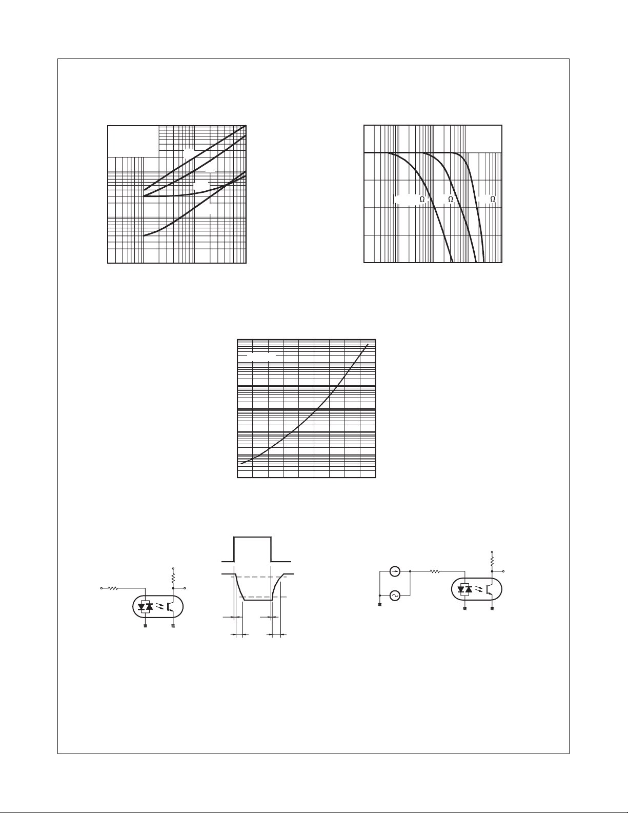
FOD814 Series, FOD617 Series, FOD817 Series 4-Pin High Operating Temperature Phototransistor Optocouplers
Typical Electrical/Optical Characteristics (Continued) (T
Fig. 13 Response Time
100
50
20
10
5
2
1
RESPONSE TIME (µs)
0.5
0.2
0.1
vs. Load Resistance
V = 2V
CE
Ic = 2m A
Ta = 25°C
0.1
0.2 0.5 1 2 5 10
LOAD RESISTANCE RL (kΩ)
tr
td
tf
ts
10000
(nA)
1000
CEO
0
(dB)
V
-10
VOLTA GE GAIN A
-20
0.2
Fig. 15 Collector Dark Current
vs. Ambient Temperature
VCE = 20V
= 25°C Unless otherwise specified.)
A
Fig. 14 Frequency Response
V
= 2V
CE
Ic = 2mA
Ta = 25°C
R =10k
L
15 20.5
FREQUENCY f (kHz)
1k
100
100010010
Test Circuit for Response Time
Vc c
R
Input
R
D
L
Output
100
10
1
0.1
0.01
COLLECTOR DARK CURRENT I
-60 -40 -20 0 20 40 60 80 100 120
AMBIENT TEMPERATURE TA (°C)
Input
Output
10%
90%
td
ts
tr tf
Test Circuit for Frequency Response
Vc c
R
R
D
L
Output
FOD814 Series, FOD617 Series, FOD817 Series Rev. 1.0.5
7 www.fairchildsemi.com
Page 8
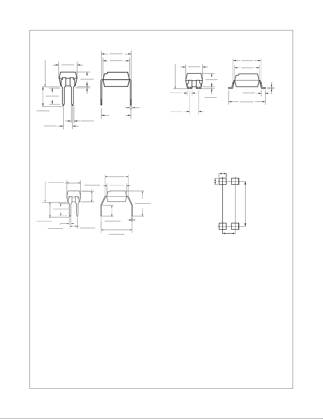
Package Dimensions (Through Hole) Package Dimensions (Surface Mount)
0.312 (7.92)
0.288 (7.32)
E
SEATING PLAN
0.150 (3.80)
0.110 (2.80)
0.110 (2.79)
0.090 (2.29)
0.130 (3.30)
0.091 (2.30)
0.200 (5.10)
0.161 (4.10)
0.157 (4.00)
0.118 (3.00)
0.020 (0.51)
TYP
0.024 (0.60)
0.016 (0.40)
0.276 (7.00)
0.236 (6.00)
0.300 (7.62)
typ
0.010 (0.26)
0.200 (5.10)
E
0.161 (4.10)
G PLAN
N
SEATI
0.051 (1.30)
0.043 (1.10)
0.110 (2.79)
0.090 (2.29)
Lead Coplanarity 0.004 (0.10) MAX
0.157 (4.00)
0.118 (3.00)
0.024 (0.60)
0.004 (0.10)
0.312 (7.92)
0.288 (7.32)
0.276 (7.00)
0.236 (6.00)
0.049 (1.25)
0.030 (0.76)
0.412 (10.46)
0.388 (9.86)
Footprint Dimensions
Package Dimensions
(0.4” Lead Spacing)
0.312 (7.92)
0.288 (7.32)
0.276 (7.00)
0.236 (6.00)
0.110 (2.80)
0.011 (1.80)
0.42 (10.66)
0.38 (9.66)
E
N
PLA
ING
T
A
SE
0.150 (3.80)
0.110 (2.80)
0.200 (5.10)
0.161 (4.10)
0.130 (3.30)
0.091 (2.30)
0.024 (0.60)
0.016 (0.40)
0.157 (4.00)
0.118 (3.00)
0.110 (2.79)
0.090 (2.29)
Note:
All dimensions are in inches (millimeters).
0.291 (7.40)
0.252 (6.40)
0.010 (0.26)
(Surface Mount)
1.5
1.3
9
2.54
FOD814 Series, FOD617 Series, FOD817 Series 4-Pin High Operating Temperature Phototransistor Optocouplers
0.010 (0.26)
FOD814 Series, FOD617 Series, FOD817 Series Rev. 1.0.5
8 www.fairchildsemi.com
Page 9
Ordering Information
Option Part Number Example Description
S FOD814S Surface Mount Lead Bend
SD FOD814SD Surface Mount; Tape and reel
W FOD814W 0.4" Lead Spacing
300 FOD814300 VDE Approved
300W FOD814300W VDE Approved, 0.4" Lead Spacing
3S FOD8143S VDE Approved, Surface Mount
3SD FOD8143SD VDE Approved, Surface Mount, Tape & Reel
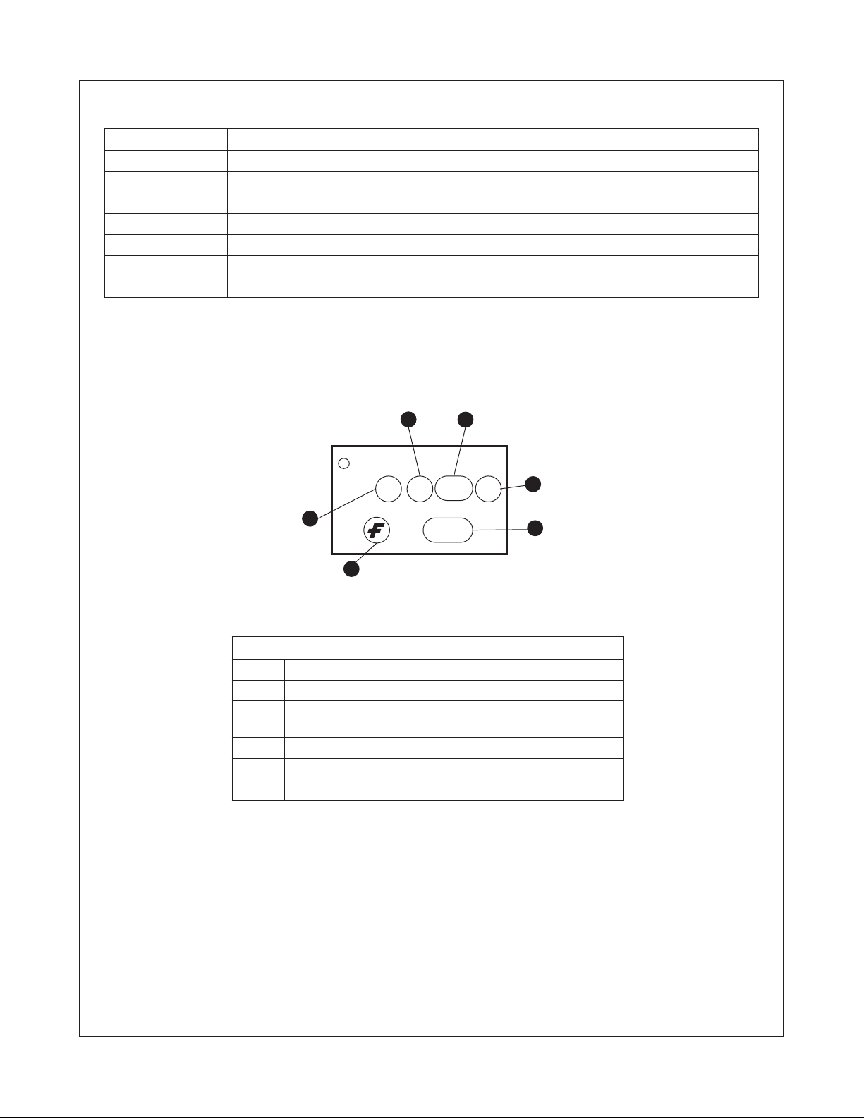
Marking Information
FOD814 Series, FOD617 Series, FOD817 Series 4-Pin High Operating Temperature Phototransistor Optocouplers
4
XVY
3
1
ZZ
814
5
6
2
Definitions
1Fairchild logo
2Device number
3 VDE mark (Note: Only appears on parts ordered with VDE
option – See order entry table)
4 One digit year code
5Two digit work week ranging from ‘01’ to ‘53’
6 Assembly package code
FOD814 Series, FOD617 Series, FOD817 Series Rev. 1.0.5
9 www.fairchildsemi.com
Page 10
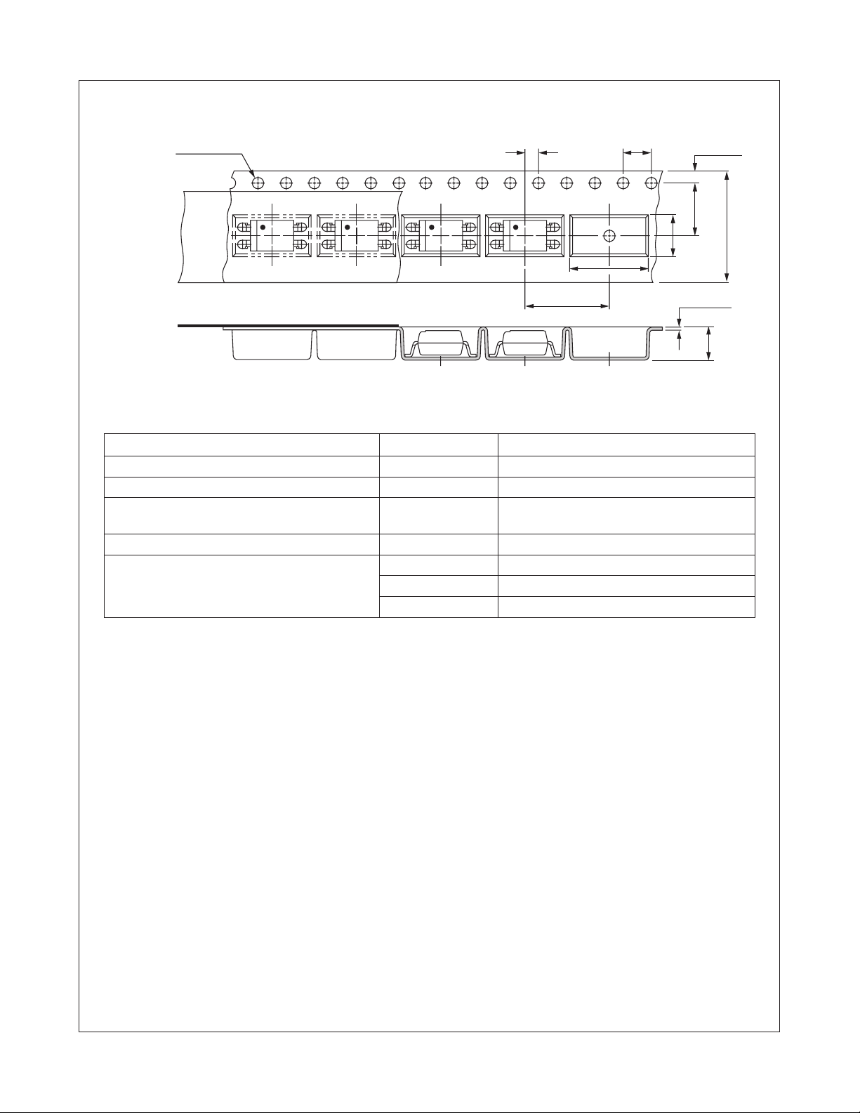
Carrier Tape Specifications
FOD814 Series, FOD617 Series, FOD817 Series 4-Pin High Operating Temperature Phototransistor Optocouplers
Ø1.55±0.05
P
2
P
1
A0
P
0
Note:
All dimensions are in millimeters.
Description Symbol Dimensions in mm (inches)
Tape wide W 16 ± 0.3 (.63)
Pitch of sprocket holes P
0
Distance of compartment F
P
2
Distance of compartment to compartment P
1
Compartment A0 10.45 ± 0.1 (.411)
B0 5.30 ± 0.1 (.209)
K0 4.25 ± 0.1 (.167)
4 ± 0.1 (.15)
7.5 ± 0.1 (.295)
2 ± 0.1 (.079)
12 ± 0.1 (.472)
1.75±0.1
F
W
B0
0.3±0.05
K0
FOD814 Series, FOD617 Series, FOD817 Series Rev. 1.0.5
10 www.fairchildsemi.com
Page 11
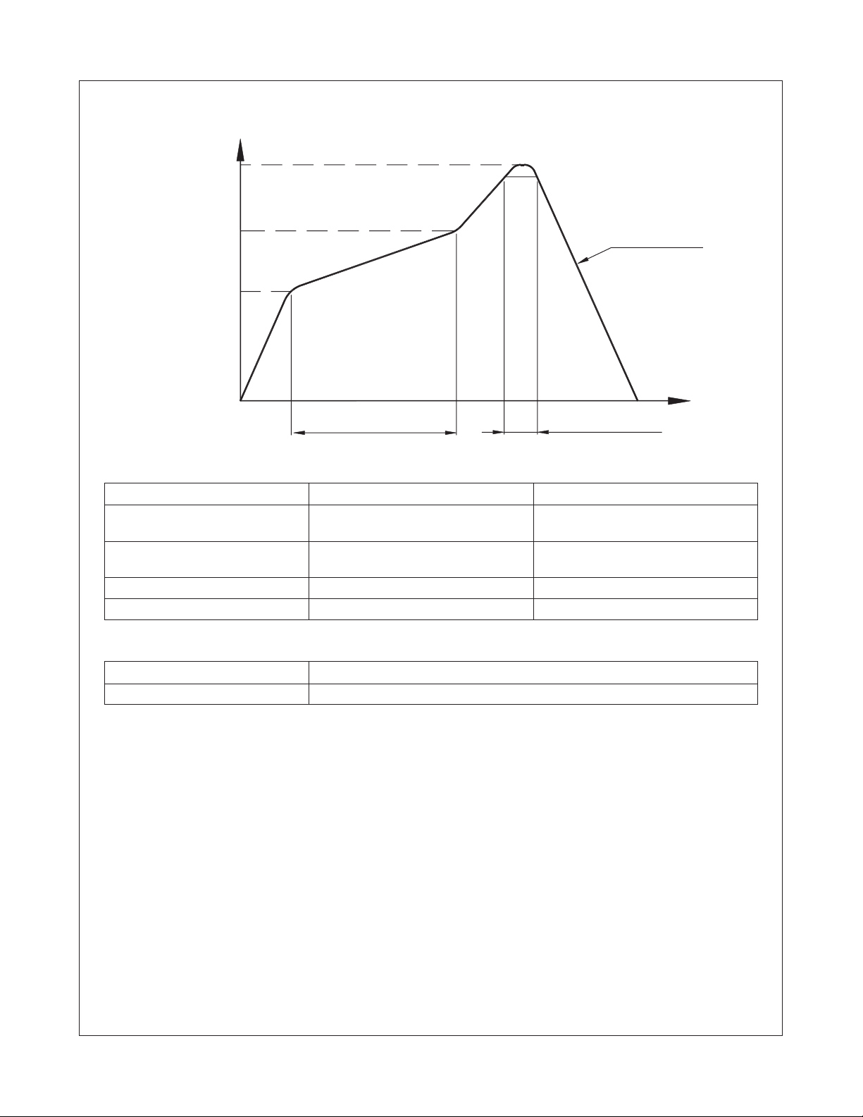
Lead Free Recommended IR Reflow Condition
Tp
FOD814 Series, FOD617 Series, FOD817 Series 4-Pin High Operating Temperature Phototransistor Optocouplers
Tsmax
Ramp-down
Tsmin
Temperature (°C)
25°C
ts (Preheat)
Soldering zon
Time (sec)
Profile Feature Pb-Sn solder assembly Lead Free assembly
Preheat condition
(Tsmin-Tsmax / ts)
Melt soldering zone 183°C
Peak temperature (Tp) 240 +0/-5°C 260 +0/-5°C
Ramp-down rate 6°C/sec max. 6°C/sec max.
100°C ~ 150°C
60 ~ 120 sec
60 ~ 120 sec
150°C ~ 200°C
60 ~120 sec
217°C
30 ~ 90 sec
Recommended Wave Soldering condition
Profile Feature For all solder assembly
Peak temperature (Tp) Max 260°C for 10 sec
FOD814 Series, FOD617 Series, FOD817 Series Rev. 1.0.5
11 www.fairchildsemi.com
Page 12

TRADEMARKS
The following are registered and unregistered trademarks Fairchild Semiconductor owns or is authorized to use and is not
intended to be an exhaustive list of all such trademarks.
ACEx™
ActiveArray™
Bottomless™
Build it Now™
CoolFET™
CROSSVOLT™
DOME™
EcoSPARK™
2
CMOS™
E
EnSigna™
FACT™
®
FAST
FASTr™
FPS™
FRFET™
GlobalOptoisolator™
GTO™
HiSeC™
2
C™
I
i-Lo™
ImpliedDisconnect™
IntelliMAX™
FACT Quiet Series™
Across the board. Around the world.™
The Power Franchise
®
Programmable Active Droop™
ISOPLANAR™
LittleFET™
MICROCOUPLER™
MicroFET™
MicroPak™
MICROWIRE™
MSX™
MSXPro™
OCX™
OCXPro™
OPTOLOGIC
®
OPTOPLANAR™
PACMAN™
POP™
Power247™
PowerEdge™
PowerSaver™
PowerTrench
QFET
®
®
QS™
QT Optoelectronics™
Quiet Series™
RapidConfigure™
RapidConnect™
µSerDes™
ScalarPump™
SILENT SWITCHER
SMART START™
SPM™
Stealth™
SuperFET™
SuperSOT™-3
SuperSOT™-6
SuperSOT™-8
SyncFET™
TCM™
TinyLogic
TINYOPTO™
TruTranslation™
UHC™
UniFET™
®
UltraFET
VCX™
Wire™
®
®
DISCLAIMER
FAIRCHILD SEMICONDUCTOR RESERVES THE RIGHT TO MAKE CHANGES WITHOUT FURTHER NOTICE TO ANY
PRODUCTS HEREIN TO IMPROVE RELIABILITY, FUNCTION OR DESIGN. FAIRCHILD DOES NOT ASSUME ANY
LIABILITY ARISING OUT OF THE APPLICATION OR USE OF ANY PRODUCT OR CIRCUIT DESCRIBED HEREIN;
NEITHER DOES IT CONVEY ANY LICENSE UNDER ITS PATENT RIGHTS, NOR THE RIGHTS OF OTHERS. THESE
SPECIFICATIONS DO NOT EXPAND THE TERMS OF FAIRCHILDíS WORLDWIDE TERMS AND CONDITIONS,
SPECIFICALLY THE WARRANTY THEREIN, WHICH COVERS THESE PRODUCTS.
FOD814 Series, FOD617 Series, FOD817 Series 4-Pin High Operating Temperature Phototransistor Optocouplers
LIFE SUPPORT POLICY
FAIRCHILDíS PRODUCTS ARE NOT AUTHORIZED FOR USE AS CRITICAL COMPONENTS IN LIFE SUPPORT
DEVICES OR SYSTEMS WITHOUT THE EXPRESS WRITTEN APPROVAL OF FAIRCHILD SEMICONDUCTOR
CORPORATION.
As used herein:
1. Life support devices or systems are devices or systems
which, (a) are intended for surgical implant into the body,
or (b) support or sustain life, or (c) whose failure to perform
when properly used in accordance with instructions for use
2. A critical component is any component of a life support
device or system whose failure to perform can be
reasonably expected to cause the failure of the life support
device or system, or to affect its safety or effectiveness.
provided in the labeling, can be reasonably expected to
result in significant injury to the user.
PRODUCT STATUS DEFINITIONS
Definition of Terms
Datasheet Identification Product Status Definition
Advance Information Formative or In
Design
Preliminary First Production This datasheet contains preliminary data, and
No Identification Needed Full Production This datasheet contains final specifications. Fairchild
This datasheet contains the design specifications for
product development. Specifications may change in
any manner without notice.
supplementary data will be published at a later date.
Fairchild Semiconductor reserves the right to make
changes at any time without notice in order to improve
design.
Semiconductor reserves the right to make changes at
any time without notice in order to improve design.
Obsolete Not In Production This datasheet contains specifications on a product
FOD814 Series, FOD617 Series, FOD817 Series Rev. 1.0.5
that has been discontinued by Fairchild semiconductor.
The datasheet is printed for reference information only.
Rev. I19
12 www.fairchildsemi.com
 Loading...