

Page 1
FOD2743A FOD2743B FOD2743C
DESCRIPTION
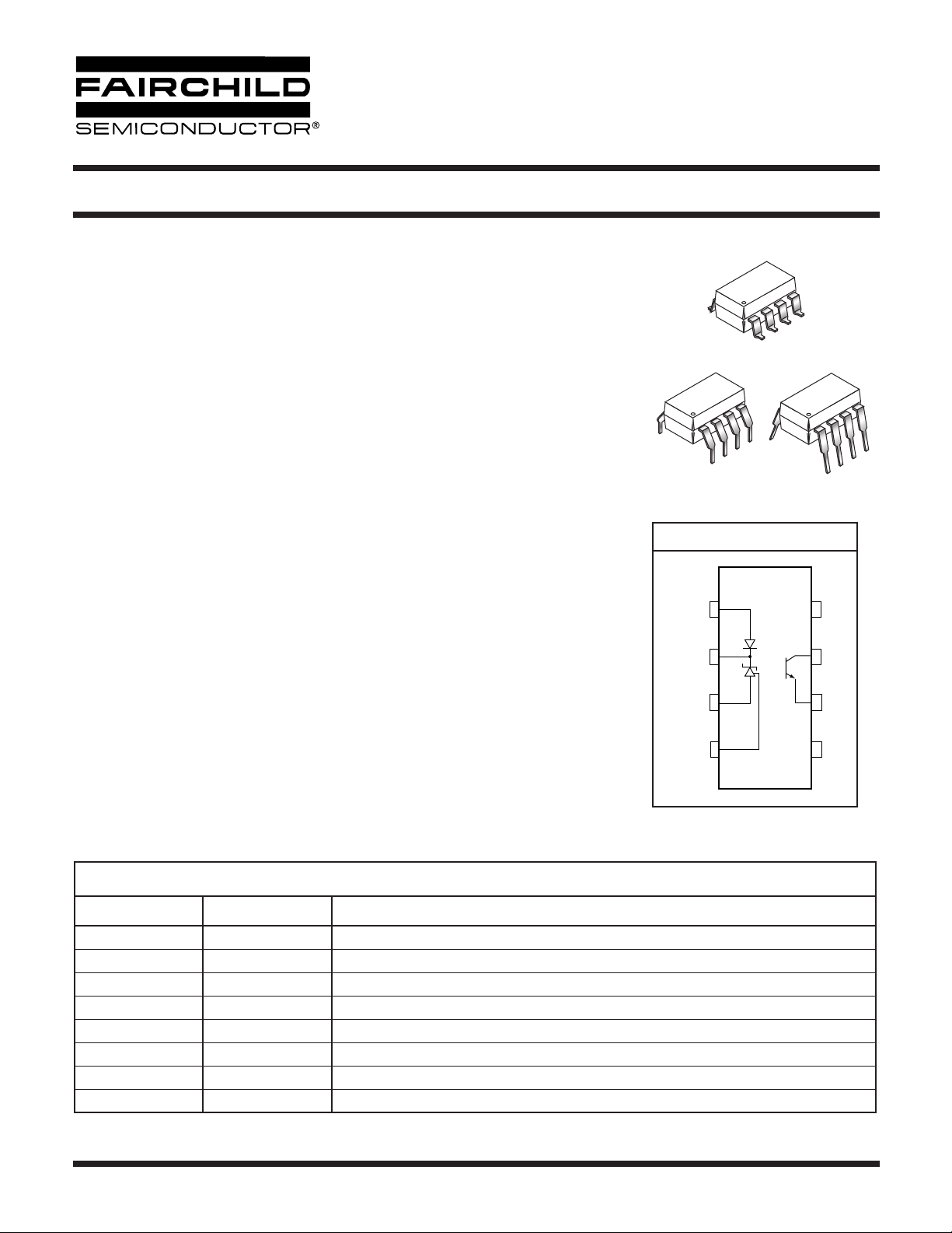
The FOD2743 Optically Isolated Amplifier consists of the popular KA431 precision
programmable shunt reference and an optocoupler. The optocoupler is a gallium arsenide
(GaAs) light emitting diode optically coupled to a silicon phototransistor. It comes in 3
grades of reference voltage tolerance = 2%, 1%, and 0.5%.
The Current Transfer Ratio (CTR) ranges from 50% to 100%. It also has an outstanding
temperature coefficient of 50 ppm/°C. It is primarily intended for use as the error amplifier/
reference voltage/optocoupler function in isolated ac to dc power supplies and dc/dc converters.
When using the FOD2743, power supply designers can reduce the component count and
save space in tightly packaged designs. The tight tolerance reference eliminates the need
for adjustments in many applications. The device comes in a 8-pin dip white package.
OPTICALLY ISOLATED
ERROR AMPLIFIER
8
1
8
1
8
1
FEATURES
• Optocoupler, precision reference and error amplifier in single package
• 2.5V reference
• CTR 50% to 100% at 1mA
• 5,000V RMS isolation
• UL approval E90700, Vol. 2
CSA approval 1296837
VDE approval pending
BSI approval pending
•Low temperature coefficient 50 ppm/°C max
• FOD2743A: tolerance 0.5%
FOD2743B: tolerance 1%
FOD2743C: tolerance 2%
APPLICATIONS
•Power supplies regulation
• DC to DC converters
PIN DEFINITIONS
Pin Number Pin Name Pin function description
1 LED Anode LED. This pin is the input to the light emitting diode.
2 COMP Error Amplifier Compensation. This pin is the output of the error amplifier. *
3 GND Ground
4FBVoltage Feedback. This pin is the inverting input to the error amplifier
5NCNot connected
6EPhototransistor Emitter
7CPhototransistor Collector
8NCNot connected
FUNCTIONAL BLOCK DIAGRAM
1
LED
COMP
2
3
GND
4 5
FB
8
NC
7
C
6
E
NC
* The compensation network must be attached between pins 2 and 4.
© 2004 Fairchild Semiconductor Corporation
Page 1 of 15
4/8/04
Page 2
OPTICALLY ISOLATED
ERROR AMPLIFIER
FOD2743A FOD2743B FOD2743C
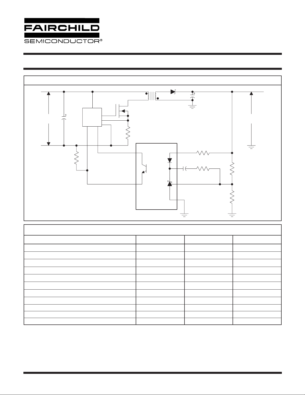
TYPICAL APPLICATION
FAN4803
V
1
PWM
Control
FOD2743
V
O
7
6
ABSOLUTE MAXIMUM RATINGS
Parameter Symbol Value Units
Storage Temperature
Operating Temperature
Lead Solder Temperature
Input Voltage
Input DC Current
Collector-Emitter Voltage
Emitter-Collector Voltage
Collector Current
Input Power Dissipation PD1 145 mW
Tr ansistor Power Dissipation PD2 85 mW
Total Power Dissipation (note 1) PD3 145 mW
Notes
1. See derating graph fig 21.
2. Functional operation under these conditions is not implied. Permanent damage may occur if the device is subjected to conditions
outside these ratings.
(T
= 25°C Unless otherwise specified.)
A
T
STG
T
OPR
T
SOL
V
LED
I
LED
V
CEO
V
ECO
I
1
2
4
3
-40 to +125 °C
-25 to +85 °C
260 for 10 sec. °C
37 V
20 mA
70 V
7V
C
50 mA
R1
R2
© 2004 Fairchild Semiconductor Corporation
Page 2 of 15
4/8/04
Page 3
/ ∆
∆
∆
/ ∆
∆
OPTICALLY ISOLATED
ERROR AMPLIFIER
FOD2743A FOD2743B FOD2743C
ELECTRICAL CHARACTERISTICS
(T
= 25°C Unless otherwise specified.)
A
INPUT CHARACTERISTICS
Parameter Test Conditions Symbol Device Min. Typ. Max. Unit
(I
LED Forward Voltage
Reference Voltage
Deviation of V
REF
over
temperature
Ratio of V
variation to the
REF
output of the error amplifier
Feedback Input Current
Deviation of I
REF
over
temperature
Minimum Drive Current
Off-state error amplifier current
Error amplifier output impedance
(see note 2)
I
LED
V
LED
= 1 mA
COMP
= 1 mA, V
I
= 1 mA, V
LED
V
I
= 1mA, R
LED
V
= 37V, V
LED
= V
, I
REF
= V
COMP
T
= -25°C to +85°C V
A
COMP
V
COMP
1
= -25°C to +85°C I
T
A
V
COMP
= 1mA to 20mA,
LED
) (fig.1) V
FB
= V
COMP
= 10V to V
= 36V to 10V
= 10k Ω (fig 3) I
= V
(fig.1) I
FB
= 0 (fig 4.) I
FB
f ≥ 1.0 kHz
FB
REF
F
V
REF
REF (DEV)
V
REF
V
COMP
REF
REF (DEV)
LED (MIN)
(OFF)
|
|Z
OUT
ALL 1.07 1.2 V
A 2.482 2.495 2.508 V
B 2.470 2.495 2.520 V
C 2.450 2.500 2.550 V
ALL 4.5 17 mV
ALL
-0.4 -2.7
-0.3 -2.0
mV/
V
ALL 2 4 µA
ALL 1 1.2 µA
ALL 0.45 1.0 mA
ALL 0.001 1.0 µA
ALL 0.15 0.5 Ω
1. The deviation parameters V
REF(DEV)
and I
REF(DEV)
are defined as the differences between the maximum and minimum values
obtained over the rated temperature range. The average full-range temperature coefficient of the reference input voltage, ∆ V
is defined as:
A
OUT
25°C=(){}106×
| = ∆ V
COMP
I
. When the device is operating with two external resistors (see
LED
V
∆V
REF
where ∆ T
ppm/°C()
is the rated operating free-air temperature range of the device.
A
REF DEV()/VREFTA
-----------------------------------------------------------------------------------------------------=
∆T
2. The dynamic impedance is defined as |Z
Figure 2), the total dynamic impedance of the circuit is given by:
Z
OUT, TOT
∆V
=
--------Z
∆I
OUT
R1
1
--------+×≈
R2
REF
,
© 2004 Fairchild Semiconductor Corporation
Page 3 of 15
4/8/04
Page 4

OPTICALLY ISOLATED
ERROR AMPLIFIER
FOD2743A FOD2743B FOD2743C
OUTPUT CHARACTERISTICS
(T
= 25°C Unless otherwise specified.)
A
Parameter Test Conditions Symbol Min Typ Max Unit
(V
Collector dark current
Emitter-collector voltage breakdown
Collector-emitter voltage breakdown
TRANSFER CHARACTERISTICS
(T
= 10 V) (Fig. 5) I
CE
(I
= 100 µA) BV
E
(I
= 1.0mA) BV
C
= 25°C Unless otherwise specified.)
A
CEO
ECO
CEO
150nA
710 V
70 100 V
Parameter Test Conditions Symbol Min Typ Max Unit
(I
(I
LED
LED
Current transfer ratio
Collector-emitter
saturation voltage
ISOLATION CHARACTERISTICS
= 1 mA, V
V
CE
= 1 mA, V
I
= 0.1 mA) (Fig. 6)
C
(T
= 25°C Unless otherwise specified.)
A
= V
COMP
FB
= 5 V) (Fig. 6)
= V
COMP
FB,
,
CTR 50 100 %
V
CE
(SAT)
0.4 V
Parameter Test Conditions Symbol Min Typ Max Unit
Input-output insulation
leakage current
Withstand insulation
voltage
Resistance (input to output)
(RH = 45%, T
V
= 3000 VDC) (note. 1)
I-O
(RH <= 50%, T
V
I-O
= 25°C, t = 5s,
A
= 25°C, t = 1 min)
A
(notes. 1)
= 500 VDC (note. 1) R
I
I-O
V
ISO
I-O
5000 Vrms
12
10
1.0 µA
Ohm
SWITCHING CHARACTERISTICS (T
= 25°C Unless otherwise specified.)
A
Parameter Test Conditions Symbol Min Typ Max Unit
Bandwidth (Fig. 7) BW 50 kHZ
(I
Common mode transient
immunity at output high
Common mode transient
immunity at output low
= 0 mA, Vcm = 10 V
LED
RL = 2.2 kΩ (Fig. 8) (note. 2)
(I
= 1 mA, Vcm = 10 V
LED
RL = 2.2 kΩ (Fig. 8) (note. 2)
PP
CMH 1.0 kV/µs
PP
CML 1.0 kV/µs
Notes
1. Device is considered as a two terminal device: Pins 1,2 3 and 4 are shorted together and Pins 5,6,7 and 8 are shorted together.
2. Common mode transient immunity at output high is the maximum tolerable (positive) dVcm/dt on the leading edge of the common mode impulse signal, Vcm, to assure that the output will remain high. Common mode transient immunity at output low is
the maximum tolerable (negative) dVcm/dt on the trailing edge of the common pulse signal,Vcm, to assure that the output will
remain low.
© 2004 Fairchild Semiconductor Corporation
Page 4 of 15
4/8/04
Page 5
OPTICALLY ISOLATED
ERROR AMPLIFIER
FOD2743A FOD2743B FOD2743C
I
I
(LED)
V
17
V
F
2
4
V
REF
3
6
V
R2
(LED)
1
2R1
4
V
COMP
V
REF
3
7
6
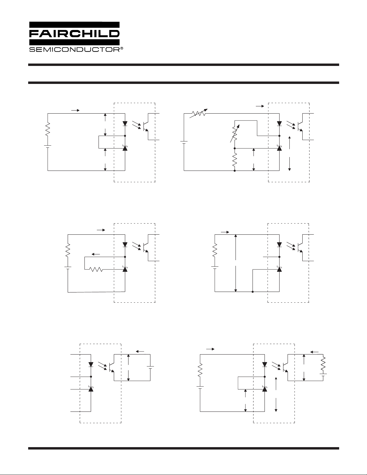
FIG. 1. V
V
, VF, I
REF
FIG. 3. I
1
2
4
3
(min) TEST CIRCUIT
LED
I
(LED)
1
I
REF
2
4
R1
3
TEST CIRCUIT
REF
7
V
6
CE
I
CEO
FIG. 2. ∆V
7
6
V
REF/∆VCOMP
I
(OFF)
V
(LED)
FIG. 4. I
I
(LED)
V
TEST CIRCUIT
(OFF)
1
2
4
V
REF
3
1
2
4
3
TEST CIRCUIT
V
COMP
7
6
I
C
7
V
CE
6
FIG. 5. I
TEST CIRCUIT FIG. 6. CTR, V
CEO
© 2004 Fairchild Semiconductor Corporation
Page 5 of 15
TEST CIRCUIT
CE(sat)
4/8/04
Page 6
OPTICALLY ISOLATED
ERROR AMPLIFIER
FOD2743A FOD2743B FOD2743C
VCC = +5V DC
= 1 mA
I
F
R
L
V
OUT
8
7
6
5
1
4
0.1 V
PP
2
3
1µf
47Ω
V
IN
0.47V
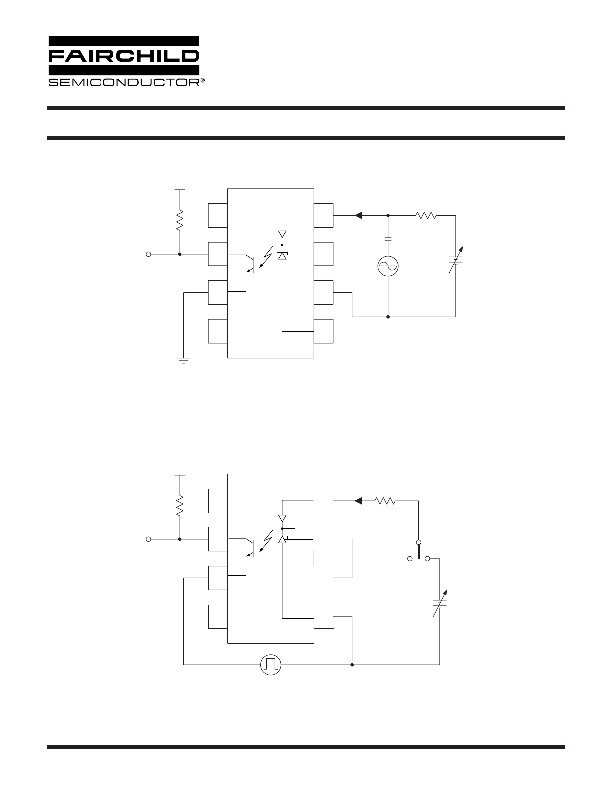
Fig. 7 Frequency Response Test Circuit
= +5V DC
V
CC
I
= 0 mA (A)
F
IF = 1 mA (B)
R1
2.2kΩ
8
1
V
OUT
© 2004 Fairchild Semiconductor Corporation
7
6
5
VCM
_
10V
+
P-P
4
2
3
Fig. 8 CMH and CML Test Circuit
Page 6 of 15
A
B
4/8/04
Page 7
OPTICALLY ISOLATED
ERROR AMPLIFIER
FOD2743A FOD2743B FOD2743C
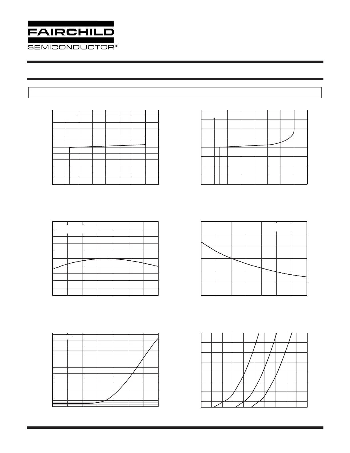
TYPICAL PERFORMANCE CURVES
15
TA = 25°C
= V
V
COMP
10
5
0
-5
- Supply Current (mA)
LED
I
-10
-15
-1 0 1 2
FB
V
- Cathode Voltage (V)
COMP
Fig. 10 – Reference Voltage Variation vs. Ambient Temperature
1.0
I
= 1mA, 10mA
LED
0.8
Fig. 9a – LED Current vs. Cathode Voltage
Normalized to T
0.6
0.4
0.2
0.0
-0.2
-0.4
- Reference Voltage Variation (%)
-0.6
REF
-0.8
∆V
-1.0
-40 -20 0 20 40 60 80 100
= 25°C
A
TA - Ambient Temperature (°C)
1.0
0.5
0.0
- Supply Current (mA)
LED
-0.5
I
- Reference Current (µA)
REF
I
-1.0
4.0
3.5
3.0
2.5
2.0
1.5
1.0
3
Fig. 9b – LED Current vs. Cathode Voltage
TA = 25°C
= V
V
COMP
FB
-1 0 1 2
- Cathode Voltage (V)
V
COMP
Fig. 11 – Reference Current vs Ambient Temperature
I
= 1mA, 10mA
LED
R1 = 10kΩ
-40 -20 0 20 40 60 80 100
T
- Ambient Temperature (°C)
A
3
Fig. 12 – Off-State Current vs. Ambient Temperature
100
VCC = 37V
10
- Off-State Current (nA)
OFF
I
1
-40 -20 0 20 40 60 80 100
TA - Ambient Temperature (°C)
© 2004 Fairchild Semiconductor Corporation
Page 7 of 15
Fig. 13 – Forward Current vs. Forward Voltage
20
15
10
- Forward Current (mA)
F
I
5
0.9 1.0 1.1 1.2
70°C
VF - Forward Voltage (V)
25°C
0°C
1.3 1.4
4/8/04
Page 8
OPTICALLY ISOLATED
ERROR AMPLIFIER
FOD2743A FOD2743B FOD2743C
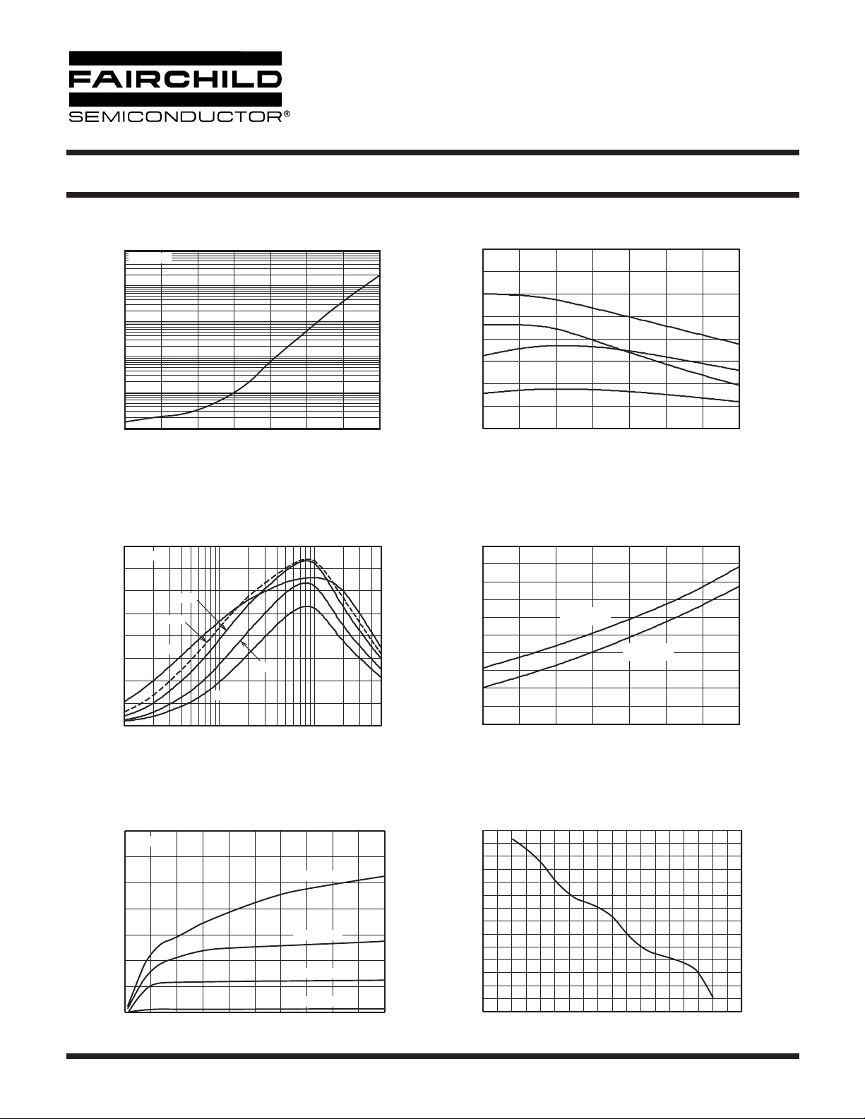
Fig. 14 – Dark Current vs. Ambient Temperature
10000
VCE = 10V
1000
100
10
- Dark Current (nA)
CEO
I
1
0.1
-40 -20 0 20 40 60 80 100
T
- Ambient Temperature (°C)
A
Fig. 16 – Current Transfer Ratio vs. LED Current
160
VCE = 5V
140
120
100
80
60
) - Current Transfer Ratio (%)
40
F
/I
C
(I
20
0
0.1 1 10
-40°C
0°C
25°C
I
LED
70°C
100°C
- Forward Current (mA)
Fig. 15 – Collector Current vs. Ambient Temperature
32
= 5V
V
CE
28
= 20mA
I
24
20
16
12
= 5, 10, 20mA
LED
I
8
- Collector Current (mA)
C
I
4
0
-40 -20 0 20 40 60 80 100
LED
= 1mA
I
LED
= 10mA
I
LED
I
= 5mA
LED
TA - Ambient Temperature (°C)
Fig. 17 – Saturation Voltage vs. Ambient Temperature
0.26
0.24
0.22
0.20
0.18
0.16
0.14
- Saturation Voltage (V)
0.12
CE(sat)
0.10
V
0.08
0.06
-40 -20 0 20 40
I
= 10mA
LED
I
= 2.5mA
C
I
LED
I
= 0.1mA
C
T
- Ambient Temperature (°C)
A
= 1mA
60 80 100
1.6
1.4
1.2
1.0
0.8
= 1mA
0.6
LED
I
0.4
- Collector Current (mA)
C
I
0.2
0.0
Fig. 18 – Collector Current vs. Collector Voltage
35
TA = 25°C
30
25
20
15
10
- Collector Current (mA)
C
I
5
0
012345678910
VCE - Collector-Emitter Voltage (V)
© 2004 Fairchild Semiconductor Corporation
I
LED
I
LED
I
LED
I
LED
= 20mA
= 10mA
= 5mA
= 1mA
Delta Vref / Delta Vout ( mV/V)
Page 8 of 15
Fig. 19 – Rate of Change Vref to Vout vs. Temperature
-0.32
-0.34
-0.36
-0.38
-0.40
-0.42
-0.44
-0.46
-60 -40 -20 0 20 40 60 80 100 120
Temperature - °C
4/8/04
Page 9
OPTICALLY ISOLATED
ERROR AMPLIFIER
FOD2743A FOD2743B FOD2743C
5
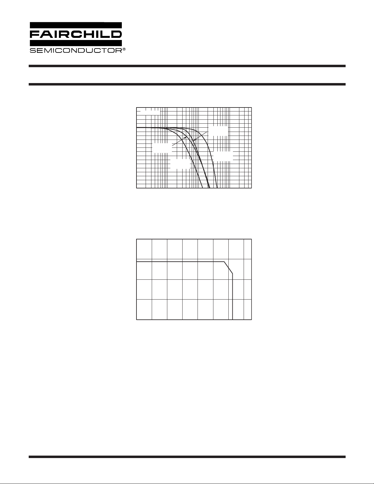
Fig. 20 – Voltage Gain vs. Frequency
V
= 10V
CC
0
= 1mA
I
-5
Voltage Gain - dB
-10
-15
200
150
F
= 2.4kΩ
R
L
= 10mA
I
F
= 1kΩ
R
L
110100 1000
Fig. 21 – Package Power Dissipation
Frequency - kHz
vs Ambient Temperature
IF = 10mA
RL = 500 Ω
I
F
R
= 10mA
= 100Ω
L
100
50
Package Power Dissipation - mW
0
-40 -20 0 20 40 60 80 100
Ta - Ambient Temperature - C
© 2004 Fairchild Semiconductor Corporation
Page 9 of 15
4/8/04
Page 10

OPTICALLY ISOLATED
ERROR AMPLIFIER
FOD2743A FOD2743B FOD2743C
The FOD2743
The FOD2743 is an optically isolated error amplifier. It incorporates three of the most common elements necessary to
make an isolated power supply, a reference voltage, an error
amplifier, and an optocoupler. It is functionally equivalent to
the popular KA431 shunt voltage regulator plus the CNY17F-X
optocoupler.
Powering the Secondary Side
The LED pin in the FOD2743 powers the secondary side, and
in particular provides the current to run the LED. The actual
structure of the FOD2743 dictates the minimum voltage that
can be applied to the LED pin: The error amplifier output has a
minimum of the reference voltage, and the LED is in series
with that. Minimum voltage applied to the LED pin is thus 2.5V
+ 1.2V = 3.7V. This voltage can be generated either directly
from the output of the converter, or else from a slaved secondary winding. The secondary winding will not affect regulation,
as the input to the FB pin may still be taken from the output
winding.
The LED pin needs to be fed through a current limiting resistor.
The value of the resistor sets the amount of current through
the LED, and thus must be carefully selected in conjunction
with the selection of the primary side resistor.
Feedback
Output voltage of a converter is determined by selecting a
resistor divider from the regulated output to the FB pin. The
FOD2743 attempts to regulate its FB pin to the reference
voltage, 2.5V. The ratio of the two resistors should thus be:
R
TOP
-------------------------R
BOTTOM
The absolute value of the top resistor is set by the input offset
current of 5.2µA. To achieve 0.5% accuracy, the resistance of
R
should be:
TOP
V
OUT
----------------------------R
TOP
V
OUT
-------------- 1–=
V
REF
2.5–
1040µA>
Compensation
The compensation pin of the FOD2743 provides the opportunity for the designer to design the frequency response of the
converter. A compensation network may be placed between
the COMP pin and the FB pin. In typical low-bandwidth
systems, a 0.1µF capacitor may be used. For converters with
more stringent requirements, a network should be designed
based on measurements of the system’s loop. An excellent
reference for this process may be found in “Practical Design of
Power Supplies” by Ron Lenk, IEEE Press, 1998.
Secondary Ground
The GND pin should be connected to the secondary ground of
the converter.
No Connect Pins
The NC pins have no internal connection. They should not
have any connection to the secondary side, as this may
compromise the isolation structure.
Photo-Transistor
The Photo-transistor is the output of the FOD2743. In a normal
configuration the collector will be attached to a pull-up resistor
and the emitter grounded. There is no base connection necessary.
The value of the pull-up resistor, and the current limiting resistor feeding the LED, must be carefully selected to account for
voltage range accepted by the PWM IC, and for the variation in
current transfer ratio (CTR) of the opto-isolator itself.
Example: The voltage feeding the LED pins is +12V, the
voltage feeding the collector pull-up is +10V, and the PWM
IC is the Fairchild FAN4803, which has a 5V reference. If we
select a 10kΩ resistor for the LED, the maximum current the
LED can see is (12V-4V) /10kΩ = 800µA. The CTR of the
opto-isolator is a minimum of 50%, so the minimum collector
current of the photo-transistor when the diode is full on is
400µA. The collector resistor must thus be such that:
10V 5V–
----------------------------------- 4 0 0 µA or R
R
COLLECTOR
COLLECTOR
12.5kΩ;><
© 2004 Fairchild Semiconductor Corporation
select 20kΩ to allow some margin.
Page 10 of 15
4/8/04
Page 11
OPTICALLY ISOLATED
0.070 (1.78)
0.060 (1.52)
0.030 (0.76)
0.100 (2.54)
0.295 (7.49)
0.415 (10.54)
ERROR AMPLIFIER
FOD2743A FOD2743B FOD2743C
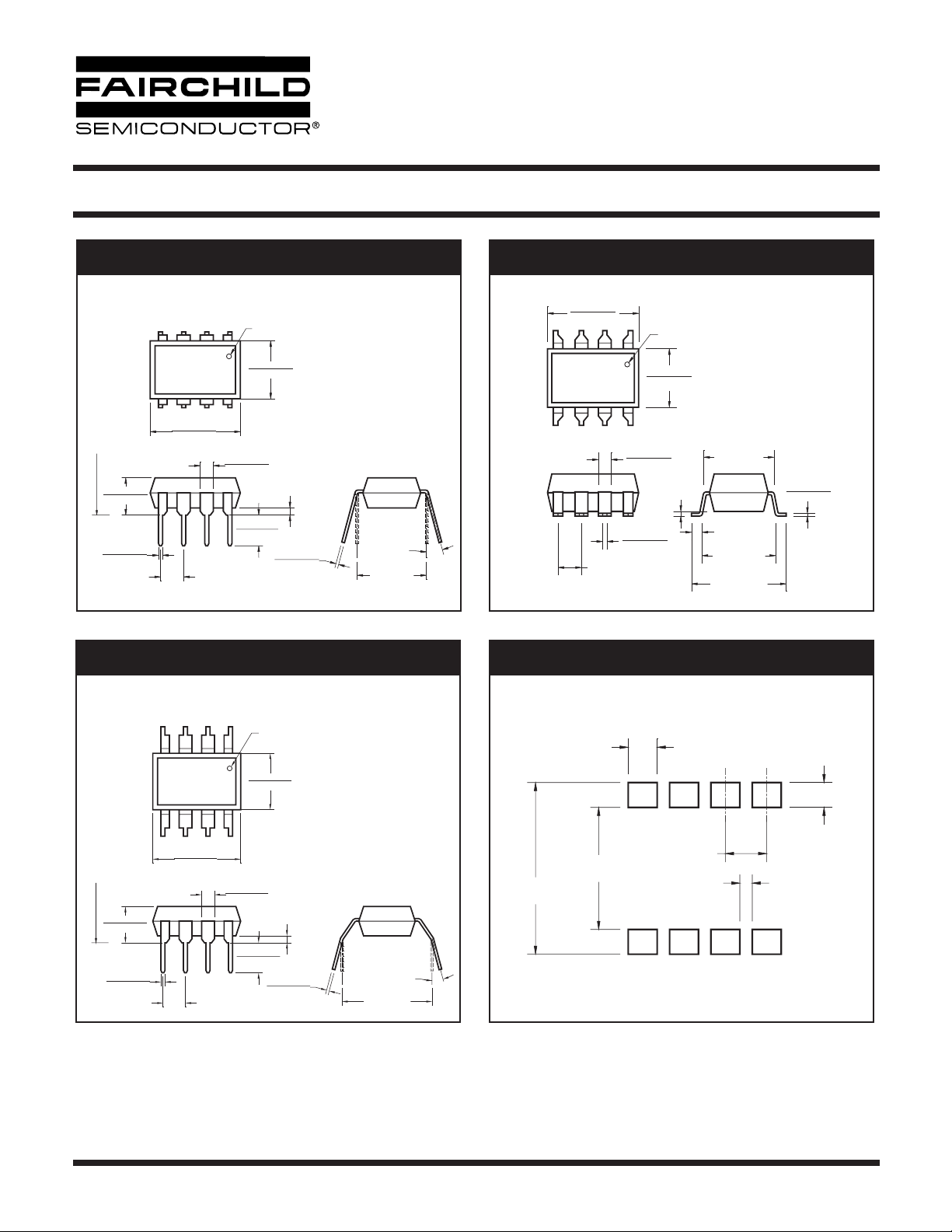
Package Dimensions (Through Hole)
PIN 1
ID.
0.270 (6.86)
0.250 (6.35)
8
0.070 (1.78)
0.045 (1.14)
0.154 (3.90)
0.120 (3.05)
0.020 (0.51) MIN
0.016 (0.40)
0.008 (0.20)
15° MAX
0.300 (7.62)
TYP
0.200 (5.08)
0.140 (3.55)
SEATING PLANE
0.022 (0.56)
0.016 (0.41)
3
241
56 7
0.390 (9.91)
0.370 (9.40)
0.100 (2.54) TYP
Package Dimensions (0.4"Lead Spacing)
Package Dimensions (Surface Mount)
0.390 (9.91)
0.370 (9.40)
3214
567
0.100 (2.54)
Lead Coplanarity : 0.004 (0.10) MAX
TYP
0.270 (6.86)
0.250 (6.35)
8
0.070 (1.78)
0.045 (1.14)
0.022 (0.56)
0.016 (0.41)
PIN 1
ID.
0.020 (0.51)
MIN
0.300 (7.62)
TYP
0.045 [1.14]
0.315 (8.00)
MIN
0.405 (10.30)
MIN
0.016 (0.41)
0.008 (0.20)
8 - Pin Dip
PIN 1
0.270 (6.86)
0.250 (6.35)
8
0.070 (1.78)
0.045 (1.14)
0.154 (3.90)
0.120 (3.05)
ID.
0.004 (0.10) MIN
0.016 (0.40)
0.008 (0.20)
0.200 (5.08)
0.140 (3.55)
SEATING PLANE
0.022 (0.56)
0.016 (0.41)
3
241
56 7
0.390 (9.91)
0.370 (9.40)
0.100 (2.54) TYP
NOTE
All dimensions are in inches (millimeters)
© 2004 Fairchild Semiconductor Corporation
0° to 15°
0.400 (10.16)
TYP
Page 11 of 15
4/8/04
Page 12
OPTICALLY ISOLATED
ERROR AMPLIFIER
FOD2743A FOD2743B FOD2743C
ORDERING INFORMATION
Example: FOD2743A X Y
X
Packaging Option
T: 0.4” Lead Spacing
S: Surface Mount Lead Bend
SD: Surface Mount Tape and Reel (1000 per reel)
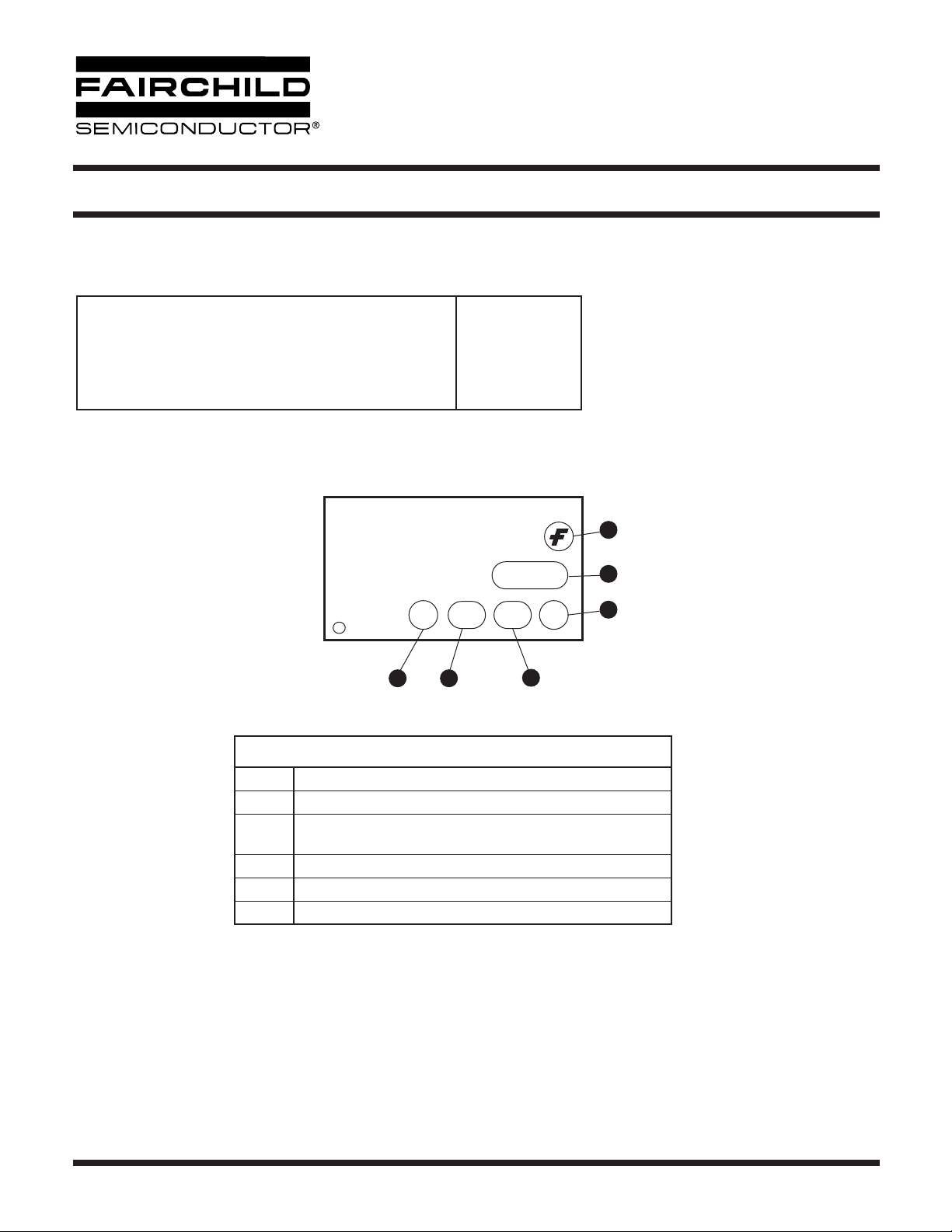
MARKING INFORMATION
Definitions
Y
V: VDE tested
XXV
43
2743A
BYY
5
1
2
6
1Fairchild logo
2Device number
VDE mark (Note: Only appears on parts ordered with VDE
3
option – See order entry table)
4Two digit year code, e.g., ‘03’
5Two digit work week ranging from ‘01’ to ‘53’
6 Assembly package code
© 2004 Fairchild Semiconductor Corporation
Page 12 of 15
4/8/04
Page 13
OPTICALLY ISOLATED
ERROR AMPLIFIER
FOD2743A FOD2743B FOD2743C
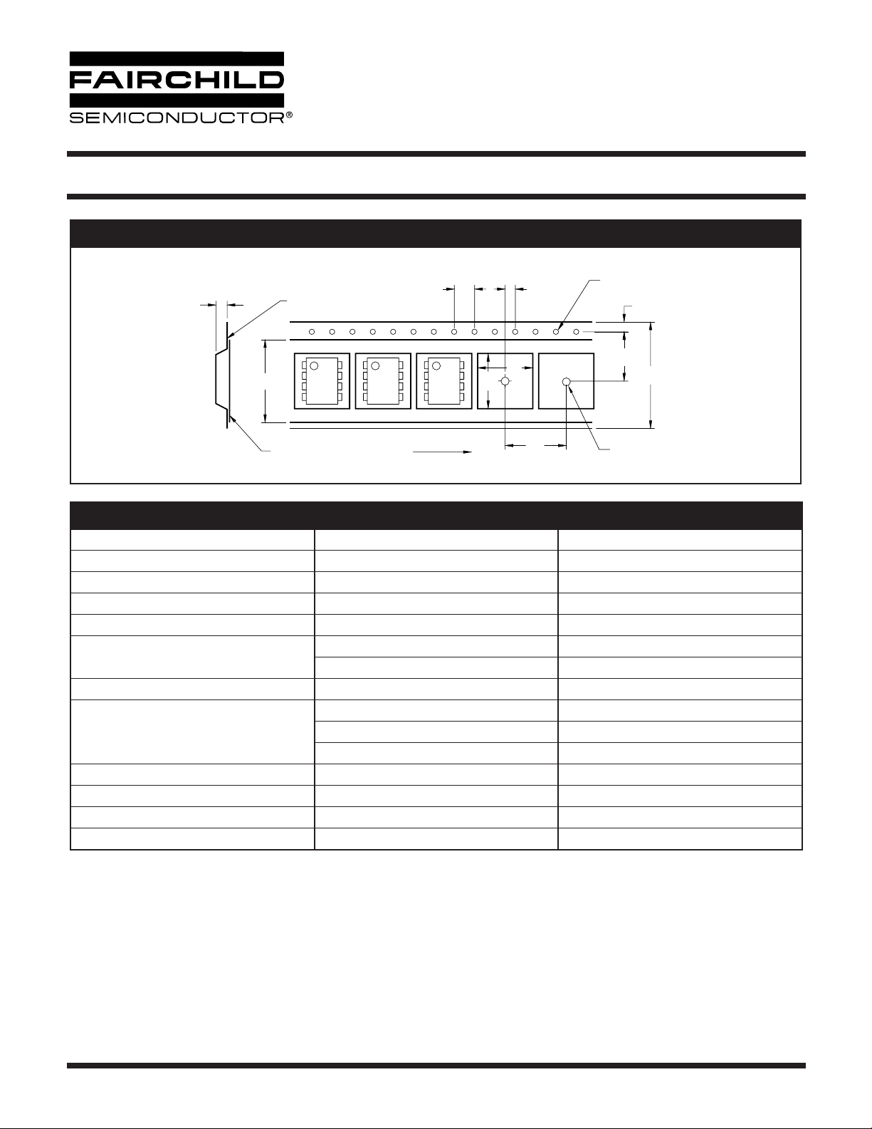
Carrier Tape Specifications
D
P
K
t
0
0
P
2
0
E
F
W
D
1
W
1
d
User Direction of Feed
A
0
B
0
P
Description Symbol Dimension in mm
Tape Width W 16.0 ± 0.3
Tape Thickness t 0.30 ± 0.05
Sprocket Hole Pitch P
Sprocket Hole Diameter D
0
0
4.0 ± 0.1
1.55 ± 0.05
Sprocket Hole Location E 1.75 ± 0.10
Pocket Location
F 7.5 ± 0.1
P
2
4.0 ± 0.1
Pocket Pitch P 12.0 ± 0.1
Pocket Dimensions
Cover Tape Width W
A
0
B
0
K
0
1
10.30 ±0.20
10.30 ±0.20
4.90 ±0.20
1.6 ± 0.1
Cover Tape Thickness d 0.1 max
Max. Component Rotation or Tilt 10°
Min. Bending Radius R 30
© 2004 Fairchild Semiconductor Corporation
Page 13 of 15
4/8/04
Page 14
OPTICALLY ISOLATED
ERROR AMPLIFIER
FOD2743A FOD2743B FOD2743C
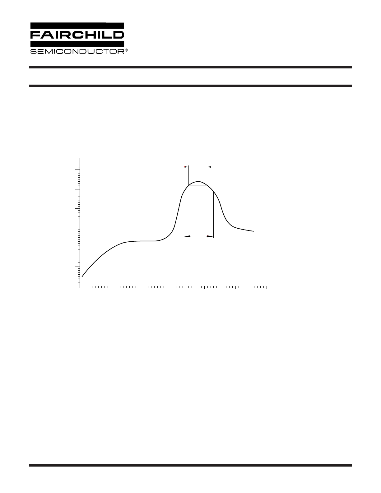
Fig. 22 Recommended IR Reflow Profile
Fig.21 Recommended IR Reflow Profile
• Peak reflow temperature 260° C (package surface temperature)
• Time of temperature higher than 245°C 40 seconds or less
• Number of reflows Three
Temperature (°C)
300
250
200
150
100
50
50 100 150
Time (s)
10 s
260°
245°
40 s
200 250
© 2004 Fairchild Semiconductor Corporation
Page 14 of 15
4/8/04
Page 15

OPTICALLY ISOLATED
ERROR AMPLIFIER
FOD2743A FOD2743B FOD2743C
DISCLAIMER
FAIRCHILD SEMICONDUCTOR RESERVES THE RIGHT TO MAKE CHANGES WITHOUT FURTHER NOTICE TO
ANY PRODUCTS HEREIN TO IMPROVE RELIABILITY, FUNCTION OR DESIGN. FAIRCHILD DOES NOT ASSUME
ANY LIABILITY ARISING OUT OF THE APPLICATION OR USE OF ANY PRODUCT OR CIRCUIT DESCRIBED HEREIN;
NEITHER DOES IT CONVEY ANY LICENSE UNDER ITS PATENT RIGHTS, NOR THE RIGHTS OF OTHERS.
LIFE SUPPORT POLICY
FAIRCHILD’S PRODUCTS ARE NOT AUTHORIZED FOR USE AS CRITICAL COMPONENTS IN LIFE SUPPORT DEVICES
OR SYSTEMS WITHOUT THE EXPRESS WRITTEN APPROVAL OF THE PRESIDENT OF FAIRCHILD SEMICONDUCTOR
CORPORATION. As used herein:
1. Life support devices or systems are devices or systems
which, (a) are intended for surgical implant into the body, or
(b) support or sustain life, and (c) whose failure to perform
when properly used in accordance with instructions for use
provided in the labeling, can be reasonably expected to
result in a significant injury of the user.
2. A critical component in any component of a life support
device or system whose failure to perform can be
reasonably expected to cause the failure of the life support
device or system, or to affect its safety or effectiveness.
© 2004 Fairchild Semiconductor Corporation
Page 15 of 15
4/8/04
 Loading...