

Page 1
www.fairchildsemi.com
FMS6414
Dual Channel Video Drivers with Integrated Filters
Video Features
• Dual Integrated Video Low Pass reconstruction filters on
outputs
• Integrated output drivers provide low impedance outputs
and deliver 2Vp-p (6dB gain) composite video into 150 Ω .
• 7.1MHz 4
• 0.4% differential gain with 0.4° differential phase
• Integrated DC Restore / Clamp Circuitry
th
order video filters
Applications
• CCTV
• Cable and Satellite Set top boxes
• DVD players
• Televisions
• HDTV
• Personal Video Recorders (PVRs)
• Video On Demand (VOD)
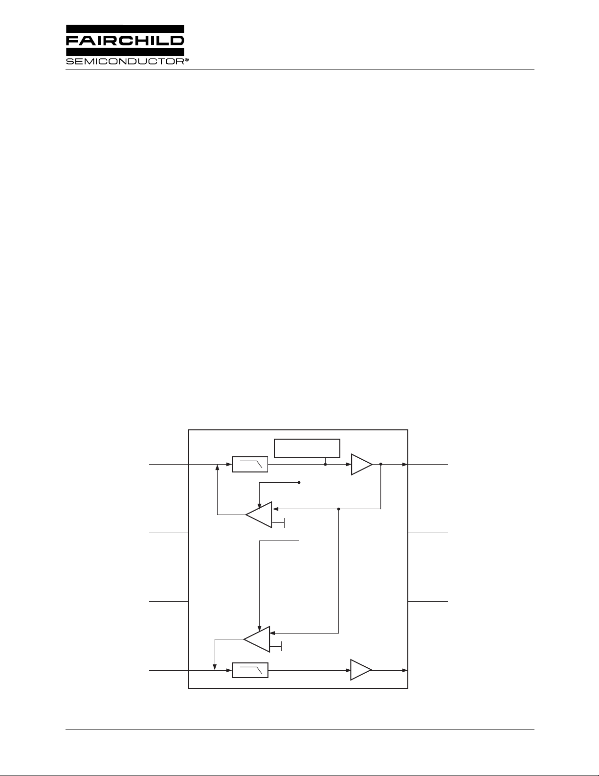
Functional Block Diagram
YIN
1
REF, AND TIMI
General Description
The FMS6414 Dual Channel Video Filter – Driver Chip
offers comprehensive video filtering for set top box or DVD
applications. This part consists of two 4
Pass Filters for video filtering. This device integrates video
drivers so that it can directly drive to the outside world.
The video signals are filtered at 7.1MHz and buffered to
drive 2Vp-p into AC coupled 150 Ω loads with up to 35pF of
load capacitance at the output pin. The filters approximate a
4th-order Butterworth characteristic with an optimization
toward low overshoot and flat group delay. Likewise, they
are capable of driving a 75 Ω load at 1Vp-p. There is an
option for the video output to be DC coupled which limits
the drive to 1 output.
SYNC STRIP,
NG
YOUT
x2
8
th
order video Low
2
NC (Reserved)
3
GND_VIDEO
4
CIN
gM
gM
1V
FMS6414
1V
VCC_VIDEO
NC (Reserved)
x2
COUT
7
6
5
REV. 1.0.1 6/27/02
Page 2
PRODUCT SPECIFICATION FMS6414
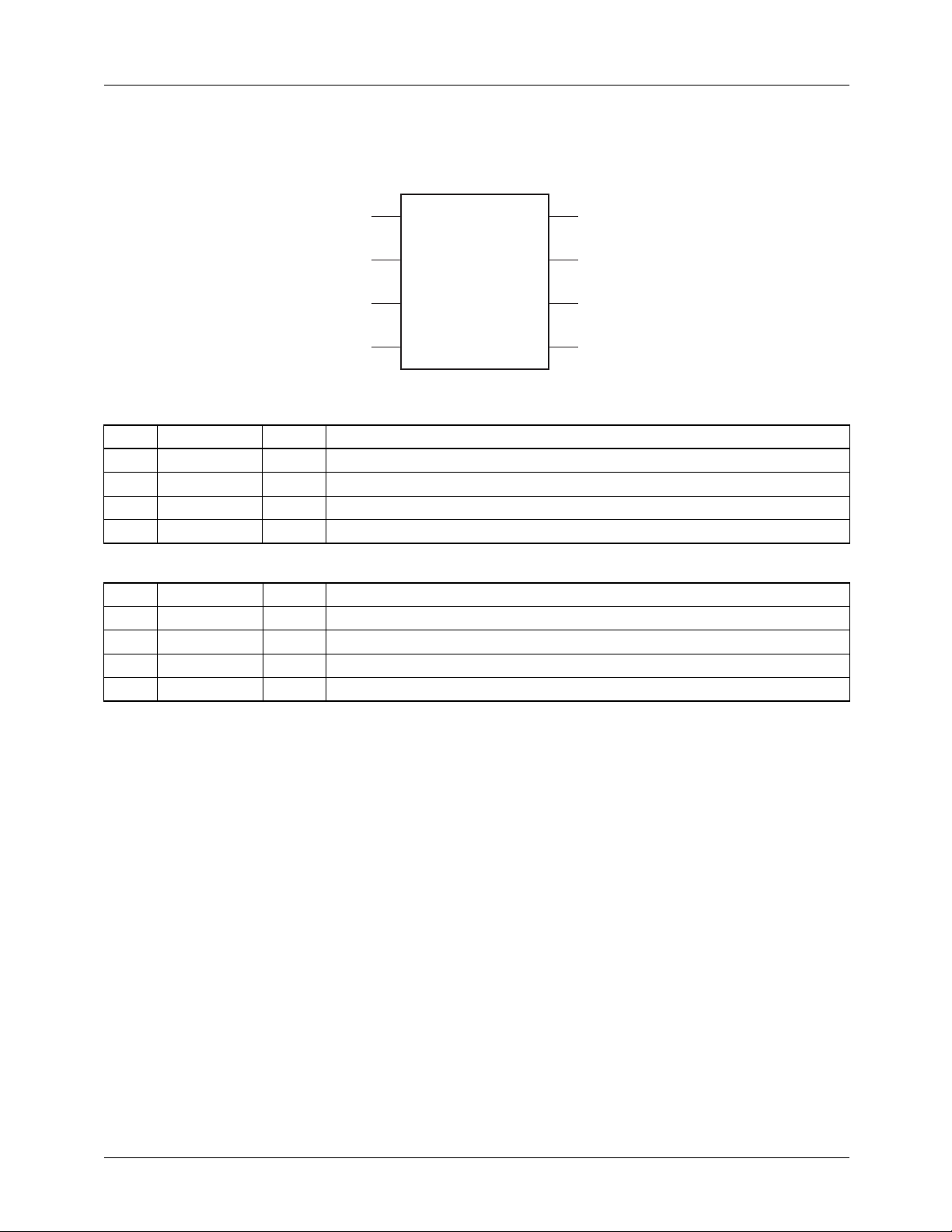
Pin Description
FMS6414
8-Pin SOIC (S08)
1
YIN
2
NC
3
GND_VIDEO
4
CIN
VCC_VIDEO
Video Section
Pin# Pin Type Description
1 YIN Input Luma (Luminance) / Composite Input
4 CIN Input Chroma (Chrominance) Input
5 COUT Output Filtered Chroma (Chrominance) Output
8 YOUT Output Filtered Luma (Luminance) Output
Power/Ground Pins
Pin# Pin Type Description
7 VCC_VIDEO Power +5 VDC for Video
3 GND_VIDEO Power Ground for Video
6 NC NC Reserved (Need to Float)
2 NC NC Reserved (Need to Float)
Y_OUT
NC
COUT
8
7
6
5
2
REV. 1.0.1 6/27/02
Page 3
FMS6414 PRODUCT SPECIFICATION
Functional Description
Introduction
The FMS6414 is a monolithic continuous time video filter
designed for reconstructing the luminance, chrominance,
or composite video signals from D/A source. The chip is
intended for use in applications with AC coupled input and
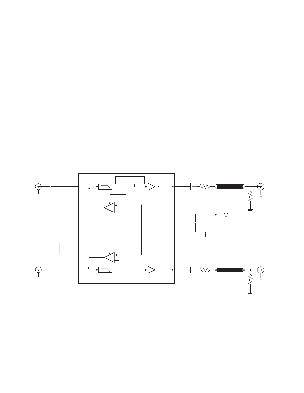
AC coupled outputs. (See Figure 1) The reconstruction filters
approximate a 4th-order Butterworth characteristic with an
optimization toward low over-shoot and flat group delay.
The video outputs are each capable of driving 2VP-P into an
AC coupled 150 Ω video load, with up to 35pF of load
capacitance at the output pin. The channel is clamped during
sync to establish the appropriate output voltage swing range.
Thus the input coupling capacitors do not behave according
to the conventional RC time constant. Clamping for all
channels settles to less than 10mv within 5ms of a change in
video input source. In most applications the input coupling
capacitors are 0.1µF. The input typically sinks 1µA during
active video, which nominally tilts a horizontal line by about
2mV at the Video output. During sync, the clamp typically
Typical Applications Diagram
YIN
0.1µF
1
YIN YOUT
SYNC STRIP,
REF, AND TIMING
sources 20µA to restore the DC level. The net result is that
the average input current is zero. Any change in the input
coupling capacitor’s value will inversely alter the amount of
tilt per line. Such a change will also linearly affect the clamp
response time. This product is robust and stable under all
stated load and input conditions. Capacitive bypassing VCC
directly to ground ensures this performance.
Video I/O
The video inputs are driven by either a low impedance
source of 1VP-P or the output of a 75 Ω terminated line.
The input is required to be AC coupled via a 0.1µF coupling
capacitor which allows for a settling time of 5ms. The video
output is capable of driving an AC coupled 150 Ω load at
2VP-P, or 1VP-P into a 75 Ω load. Up to 35pF of load
capacitance (at the output pin) can be driven without stability
or slew issues. The output is AC coupled with a 220µF or
larger AC coupling capacitor.
220µF
x2
8
75Ω
Video Cable
75Ω
YOUT
CIN
0.1µF
2
NC (Reserved)
3
GND_VIDEO
4
CIN
gM
gM
1V
FMS6414
1V
VCC_VIDEO
NC (Reserved)
x2
Figure 1.
COUT
7
0.1µF
6
220µF
5
75Ω
+5.0V
1µF
Video Cable
75Ω
COUT
REV. 1.0.1 6/27/02
3
Page 4
PRODUCT SPECIFICATION FMS6414
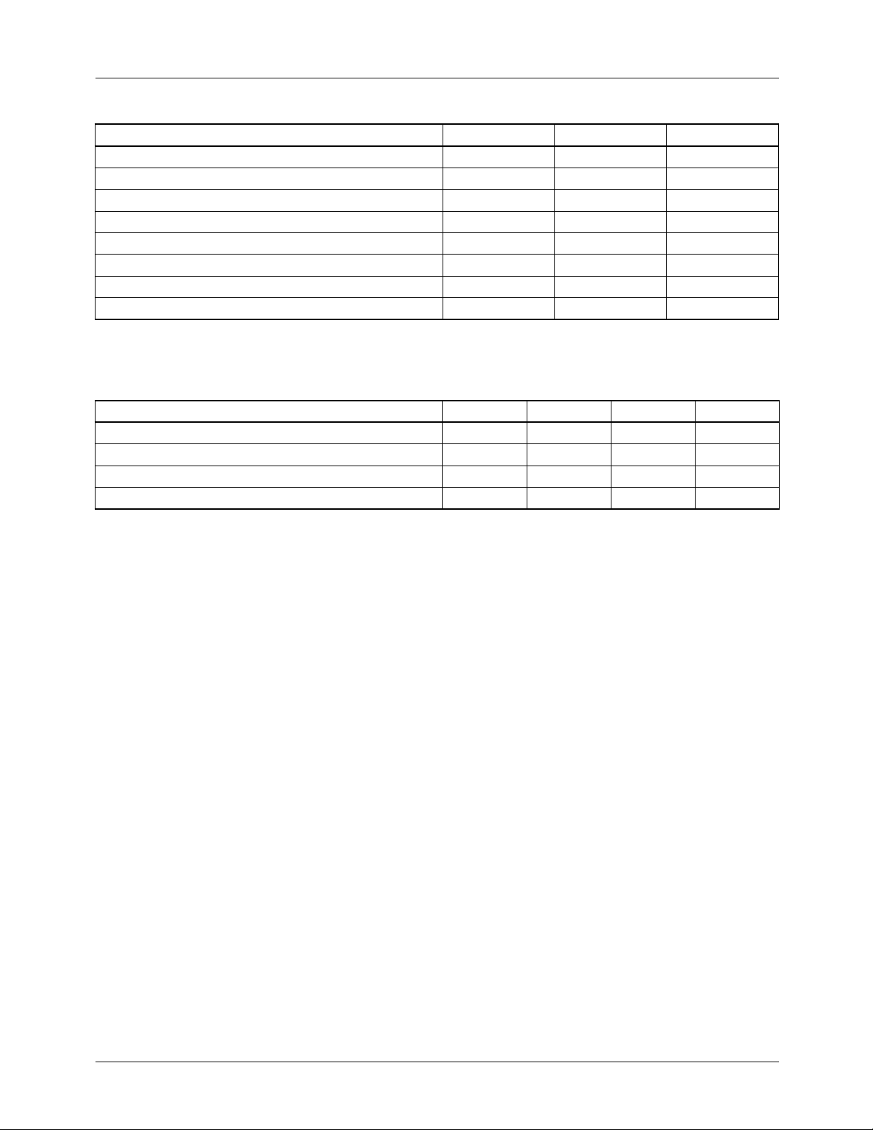
Absolute Maximum Ratings
Parameter Min Max Units
VCC_VIDEO (Positive DC Supply Voltage) +6.5 V
GND_VIDEO (Negative DC Supply Voltage) V
Analog and Digital I/O GND – 0.3 VCC + 0.3 V
Output Current (Continuous) 60 mA
Junction Temperature 150 °C
Storage Temperature Range -65 +150 °C
Lead Temperature (Soldering, 10s) 260 °C
Thermal Resistance ( Θ
Note: Functional operation under any of these conditions is NOT implied. Performance and reliability are guaranteed only if
Operating Conditions are not exceeded.
) 115 °C/W
JA
(beyond which the device may be damaged)
Operating Conditions
Parameter Min Typ Max Units
Temperature Range 0 70 °C
VCC_VIDEO Range 4.75 5.0 5.25 V
GND_VIDEO 0 V
ICC (+5 VDC) 60 mA
4
REV. 1.0.1 6/27/02
Page 5
∆
FMS6414 PRODUCT SPECIFICATION
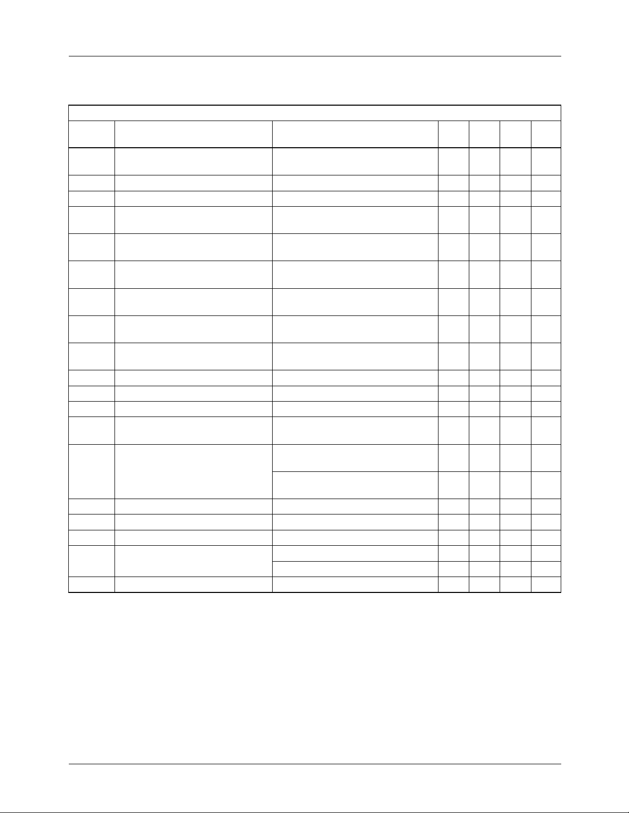
Electrical Characteristics
1Vp-p signal at room temperature
Video Characteristics – Unless otherwise noted, typical output loading on video output is 150 Ω .
Symbol Parameter Condition
VCC_VIDEO=+5.0V ±10%
AVYC Low Frequency Gain
(YOUT, COUT)
YSYNC YOUT Output Level (During Sync) Sync Present on YIN 0.75 1.0 1.25 V
CSYNC COUT Output Level (During Sync) Sync Present on YIN 1.6 2.0 2.4 V
tCLAMP Clamp Response Time
(Y Channel)
f1dB –1.0dB Bandwidth (Flatness)
(YOUT, COUT)
fC –3dB Bandwidth (Flatness)
(YOUT, COUT)
fSB Stopband Rejection
(YOUT, COUT)
Vi Input Signal Dynamic Range
(All Channels)
ISC Output Short Circuit Current
(All Channels)
CL Output Shunt Capacitance All Channels 35 pF
dG Differential Gain YOUT, COUT 0.4 %
dP Differential Phase YOUT, COUT 0.4 °
THD Output Distortion (All Channels) YOUT/ COUT = 1.8VP-P at 3.58/
XTALK Crosstalk From CIN of 0.5VP-P at 3.58MHz to
PSRR PSRR (All Channels) 0.5VP-P (100kHz) at VCC -40 dB
SNR Y, C Channel NTC-7 weighting 4.2 MHz lowpass -75 dB
tpd Group Delay (Y, C) 100kHz 70 ns
tpd Group Delay Deviation from
Flatness (Y, C)
tSKEW Skew between YOUT and COUT At 1MHz 0 ns
at 400KHz 5.75 6.0 6.25 dB
Settled to Within 10mV, 0.1µF cap
on YIN and CIN
No Peaking Cap (Note 1) 4.0 4.5 MHz
fIN = 27MHz to 100MHz worst case -37 -42 dB
AC Coupled 1.3 1.4 VP-P
YOUT, COUT to GND (Note 2) 40 80 mA
4.43MHz
YOUT
From YIN Input of 0.4VP-P at
3.58MHz, to COUT
to 3.58MHz (NTSC) 9 ns
to 4.43MHz (PAL) 7 ns
Min Typ Max Units
5ms
6.7 7.1 MHz
0.8 %
-55 dB
-58 dB
Notes:
1. Peaking capacitor increases output at 4.2MHz nominally by 0.7dB
2. Sustained short circuit protection limited to 10 seconds
REV. 1.0.1 6/27/02
5
Page 6
PRODUCT SPECIFICATION FMS6414
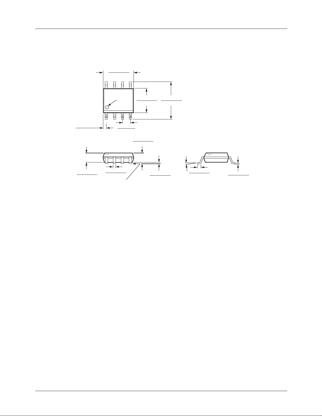
Mechanical Dimensions Inches (millimeters)
Package: S08
8-Pin SOIC
0.189 - 0.199
(4.80 - 5.06)
8
0.017 - 0.027
(0.43 - 0.69)
(4 PLACES)
0.055 - 0.061
(1.40 - 1.55)
PIN 1 ID
1
0.050 BSC
(1.27 BSC)
0.012 - 0.020
(0.30 - 0.51)
SEATING PLANE
0.148 - 0.158
(3.76 - 4.01)
0.059 - 0.069
(1.49 - 1.75)
0.228 - 0.244
(5.79 - 6.20)
0.004 - 0.010
(0.10 - 0.26)
0° - 8°
0.015 - 0.035
(0.38 - 0.89)
0.006 - 0.010
(0.15 - 0.26)
6
REV. 1.0.1 6/27/02
Page 7

PRODUCT SPECIFICATION FMS6414
Ordering Information
Part Number Temperature Range Package
FMS6414CS 0° to 70° 8 Pin SOIC (S08)
FMS6414CSX 0° to 70° Tape and Reel
DISCLAIMER
FAIRCHILD SEMICONDUCTOR RESERVES THE RIGHT TO MAKE CHANGES WITHOUT FURTHER NOTICE TO
ANY PRODUCTS HEREIN TO IMPROVE RELIABILITY, FUNCTION OR DESIGN. FAIRCHILD DOES NOT ASSUME
ANY LIABILITY ARISING OUT OF THE APPLICATION OR USE OF ANY PRODUCT OR CIRCUIT DESCRIBED HEREIN;
NEITHER DOES IT CONVEY ANY LICENSE UNDER ITS PATENT RIGHTS, NOR THE RIGHTS OF OTHERS.
LIFE SUPPORT POLICY
FAIRCHILD’S PRODUCTS ARE NOT AUTHORIZED FOR USE AS CRITICAL COMPONENTS IN LIFE SUPPORT DEVICES
OR SYSTEMS WITHOUT THE EXPRESS WRITTEN APPROVAL OF THE PRESIDENT OF FAIRCHILD SEMICONDUCTOR
CORPORATION. As used herein:
1. Life support devices or systems are devices or systems
which, (a) are intended for surgical implant into the body, or
(b) support or sustain life, and (c) whose failure to perform
when properly used in accordance with instructions for use
provided in the labeling, can be reasonably expected to
result in a significant injury of the user.
www.fairchildsemi.com
2. A critical component in any component of a life support
device or system whose failure to perform can be
reasonably expected to cause the failure of the life support
device or system, or to affect its safety or effectiveness.
6/27/02 0.0m 004
2002 Fairchild Semiconductor Corporation
Stock#DS30006414
 Loading...