

Page 1
www.fairchildsemi.com
FMS3818
Triple Video D/A Converter
3 x 8 bit, 180 Ms/s
Features
• ±2.5% gain matching
• ±0.5 LSB linearity error
• Internal bandgap voltage reference
• Low glitch energy
• Single 3.3 Volt power supply
Applications
• PC Graphics
• Video signal conversion
– RGB
– YC
C
B
R
– Composite, Y, C
Description
The FMS3818 is a low-cost triple D/A converter, tailored to
fit graphics and video applications where speed is critical.
CMOS-level inputs are converted to analog current outputs
that can drive 25–37.5 Ω loads corresponding to doublyterminated 50–75 Ω loads. A sync current following SYNC
input timing is added to the I
override RGB inputs, setting I
zero when BLANK
applications the internal 1.25V reference voltage can be
overridden by the V
Few external components are required, just the current
reference resistor, current output load resistors, bypass
capacitors and decoupling capacitors.
Package is a 48-lead LQFP. Fabrication technology is
CMOS. Performance is guaranteed from 0 to 70°C.
= L. Although appropriate for many
input.
REF
output. BLANK
OG
, I
OB
and I
OG
will
currents to
OR
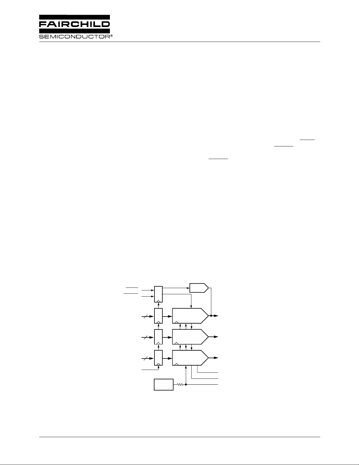
Block Diagram
SYNC
BLANK
G
7-0
B
7-0
R
7-0
CLK
SYNC
8
8
8
+1.25V
Ref
8 bit D/A
Converter
8 bit D/A
Converter
8 bit D/A
Converter
I
OS
IO
G
IO
B
IO
R
COMP
R
REF
V
REF
REV. 1.2.2 11/11/01
Page 2
FMS3818 PRODUCT SPECIFICATION
Functional Description
Within the FMS3818 are three identical 8-bit D/A
converters, each with a current source output. External loads
are required to convert these currents to voltage outputs.
Data inputs RGB
SYNC = H activates sync current from I
are overridden by the BLANK
7-0
for sync-on-
OS
green video signals.
V
DDA
I
OS
V
SYNC
G
B
R
7-0
7-0
7-0
DDA
V
DDA
V
DDA
input.
BLANK
gates the D/A inputs. If BLANK = H, the D/A
inputs control the output currents to be added to the output
blanking level. If BLANK
= L, data inputs and the pedestal
are disabled.
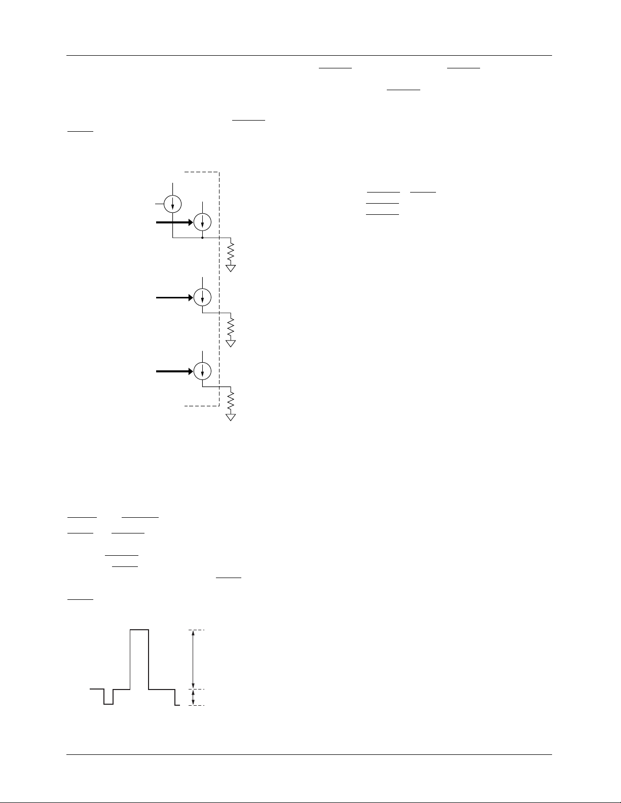
D/A Outputs
Each D/A output is a current source from the V
Expressed in current units, the GBR transformation from
data to current is as
follows:
G = G
B = B
R = R
& BLANK
7-0
& BLANK
7-0
& BLANK
7-0
+ SYNC * 112
Typical LSB current step is 73.2 µA.
To obtain a voltage output, a resistor must be connected to
ground. Output voltage depends upon this external resistor,
the reference voltage, and the value of the gain-setting resistor connected between R
and GND.
REF
To implement a doubly-terminated 75 Ω transmission line, a
shunt 75 Ω resistor should be placed adjacent to the analog
output pin. With a terminated 75 Ω line connected to the
analog output, the load on the FMS3818 current source is
37.5 Ω .
The FMS3818 may also be operated with a single 75 Ohm
terminating resistor. To lower the output voltage swing to the
desired range, the nominal value of the R
REF
be doubled.
supply.
DDA
resistor should
Figure 1. FMS3818 Current Source Structure
Digital Inputs
Incoming GBR data is registered on the rising edge of the
clock input, CLK. Analog outputs follow the rising edge of
CLK after a delay, t
and BLANK
SYNC
and BLANK inputs control the output level (Figure 1
SYNC
and Table 1) of the D/A converters during CRT retrace
intervals. BLANK
level while SYNC
connected to the green D/A converter. SYNC = H adds a
112/256 fraction of full-scale current to the green output.
SYNC = L extinguishes the sync current during the sync tip.
Figure 2. Nominal Output Levels
.
DO
forces the D/A outputs to the blanking
= L turns off a current source, I
data: 700 mV max.
sync: 307 mV
OS
that is
Voltage Reference
Full scale current is a multiple of the current I
external resistor, R
GND. Voltage across R
connected between the R
SET
is the reference voltage, V
SET
which can be derived from either the 1.25 volt internal
bandgap reference or an external voltage reference
connected to V
should be connected between V
I
is mirrored to each of the GBR output current sources.
SET
. To minimize noise, a 0.1µF capacitor
REF
and ground.
REF
To minimize noise, a 0.1µF capacitor should be connected
between the COMP pin and the analog supply voltage V
through an
SET
REF
pin and
,
REF
DDA
Power and Ground
Required power is a single +3.3 Volt supply. To minimize
power supply induced noise, analog +3.3V should be
connected to V
decoupling capacitors placed adjacent to each V
pin pair.
High slew-rate digital data makes capacitive coupling to the
outputs of any D/A converter a potential problem. Since the
digital signals contain high-frequency components of the
CLK signal, as well as the video output signal, the resulting
data feedthrough often looks like harmonic distortion or
reduced signal-to-noise performance. All ground pins should
be connected to a common solid ground plane for best
performance.
DDD
and V
pins with 0.1 and 0.01 µF
DDA
DD
pin or
.
2
REV. 1.2.2 11/11/01
Page 3
PRODUCT SPECIFICATION FMS3818
Table 1. Output Voltage Coding
V
= 1.25 V, R
REF
RGB7-0 (MSB…LSB) SYNC BLANK V
1111 1111 1 1 700 1,007
1111 1111 0 1 700 700
1111 1110 1 1 697 1,004
1111 1101 1 1 695 1,001
•
•
1000 0000 1 1 351 658
0111 1111 1 1 349 656
0111 1111 0 1 349 349
•
•
0000 0010 1 1 5 312
0000 0001 1 1 3 310
0000 0000 1 1 0 307
0000 0000 0 1 0 0
XXXX XXXX 1 0 0 307
XXXX XXXX 0 0 0 0
= 348 Ω , R
REF
= 37.5 Ω
L
•
•
•
•
, V
RED
•
•
•
•
(mV) V
BLUE
•
•
•
•
GREEN
•
•
•
•
(mV)
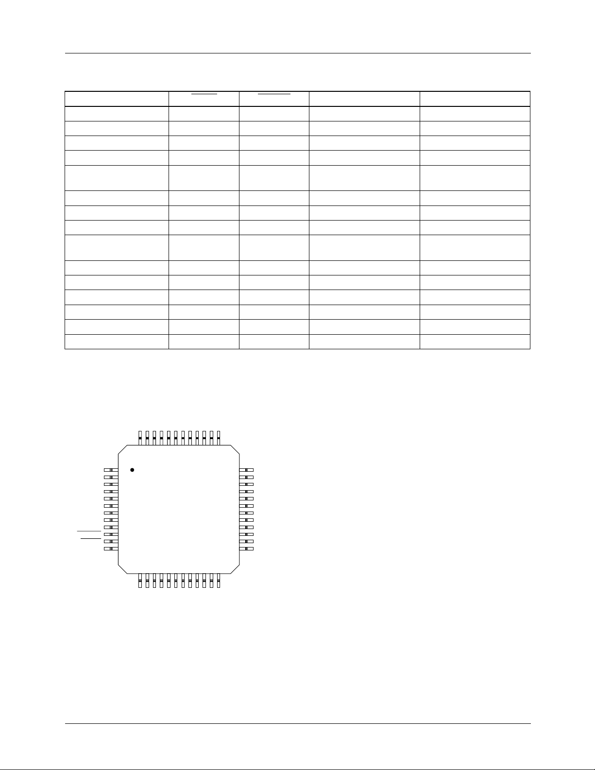
Pin Assignments
LQFP Package
GND
R7R6R5R4R3R2R
484746454443424140
GND
G
G
G
G
G
G
G
G
BLANK
SYNC
V
DDD
1
2
0
3
1
4
2
5
3
6
4
7
5
6
8
7
9
10
11
12
FMS3818
131415161718192021
NC
GND
GND
1
B0B1B2B3B4B6B
R0GND
GND
39
38
22
23
5
7
B
NC
37
24
NC
36
35
34
33
32
31
30
29
28
27
26
25
R
REF
V
REF
COMP
IO
R
IO
G
V
DDA
V
DDA
IO
B
GND
GND
CLK
NC
REV. 1.2.2 11/11/01
3
Page 4
)
FMS3818 PRODUCT SPECIFICATION
Pin Descriptions
Pin
Name Pin Number Value Pin Function Description
Clock and Data Inputs
CLK 26 CMOS Clock Input. Pixel data is registered on the rising edge of CLK. CLK
should be driven by a dedicated buffer to avoid reflection induced jitter,
overshoot, and undershoot.
R
7-0
G
7-0
B
7-0
47-40
9-2
23-16
CMOS Red, Green, and Blue Pixel Data Inputs. RGB digital inputs are
registered on the rising edge of CLK.
Controls
SYNC 11 CMOS Sync Pulse Input. Bringing SYNC LOW, disables a current source which
superimposes a sync pulse on the I
output. SYNC and pixel data are
OG
registered on the rising edge of CLK. SYNC does not override any other
data and should be used only during the blanking interval. If sync pulses
should be connected to GND.
BLANK
are not required, SYNC
10 CMOS Blanking Input. When BLANK is LOW, pixel data inputs are ignored and
the D/A converter outputs are driven to the blanking level. BLANK is
registered on the rising edge of CLK.
Video Outputs
I
I
I
OR
OG
OB
33
32
29
0.700 V
Red, Green, and Blue Current Outputs. Current source outputs can
p-p
drive VESA VSIS, and RS-343A/SMPTE-170M compatible levels into
doubly-terminated 75 Ohm lines. Sync pulses can be added to the green
output. When SYNC
is HIGH, the current added to I
OG
is:
IO
Voltage Reference
V
R
REF
REF
35 +1.25 V Voltage Reference Input/Output. Internal 1.25V voltage reference is
36 348 Ω
= 2.33 (V
S
available on this pin. An external +1.25 Volt reference may be applied to
this pin to override the internal reference. Decoupling V
a 0.1µF ceramic capacitor is required.
Current-set Resistor Node. Full-scale output current of each D/A
converter is determined by the value of the resistor connected between
R
and GND. Nominal value of R
REF
REF
/ R
REF
is found from:
REF
to GND with
REF
R
= 5.31 (V
REF
where I
is the full-scale output current (amps) from the
FS
D/A converter (without sync). Sync is 0.439 I
REF
/I
)
FS
.
FS
D/A full-scale current may also be calculated from:
I
= V
FS
Where V
/R
FS
L
is the full-scale voltage level and R
FS
is the total resistive load
L
(ohms) on each D/A converter.
COMP 34 0.1 µF Compensation Capacitor Node. A 0.1 µF ceramic capacitor must be
connected between COMP and V
4
to stabilize internal bias circuitry.
DD
REV. 1.2.2 11/11/01
Page 5

PRODUCT SPECIFICATION FMS3818
Pin Descriptions (continued)
Pin
Name Pin Number Value Pin Function Description
Power, Ground
V
DDA
V
DDD
GND 1, 14, 15, 27,
NC 13, 24, 25, 37 — No Connect
30, 31 +3.3V Analog Supply Voltage.
12 +3.3V Digital Supply Voltage.
0.0V Ground.
28, 38, 39, 48
REV. 1.2.2 11/11/01
5
Page 6

FMS3818 PRODUCT SPECIFICATION
Absolute Maximum Ratings (beyond which the device may be damaged)
1
Parameter Min Typ Max Unit
Power Supply Voltage
V
(Measured to GND) -0.5 4 V
DDA
V
(Measured to GND) -0.5 4 V
DDD
Digital Inputs
Applied Voltage (Measured to GND)
2
-0.5 V
DDD
+
0.5
Forced Current
3,4
-5.0 5.0 mA
Analog Inputs
Applied Voltage (Measured to GND)
Forced Current
3,4
2
-0.5 V
+ 0.5 V
DDA
-10.0 10.0 mA
Analog Outputs
Applied Voltage (Measured to GND)
Forced Current
3,4
2
-0.5 V
+ 0.5 V
DDA
-60.0 60.0 mA
Short Circuit Duration (single output in HIGH state to ground) unlimited sec.
Temperature
Operating, Ambient -20 110 °C
Junction 150 °C
Lead Soldering (10 seconds) 300 °C
Vapor Phase Soldering (1 minute) 220 °C
Storage -65 150 °C
Notes:
1. Functional operation under any of these conditions is NOT implied. Performance and reliability are guaranteed only if
Operating Conditions are not exceeded.
2. Applied voltage must be current limited to specified range.
3. Forcing voltage must be limited to specified range.
4. Current is specified as conventional current flowing into the device.
V
Operating Conditions
Parameter Min Nom Max Units
V
V
C
R
T
DD
REF
C
L
A
Power Supply Voltage 3.0 3.3 3.6 V
Reference Voltage, External 1.0 1.25 1.5 V
Compensation Capacitor 0.1 µF
Output Load 37.5 Ω
Ambient Temperature, Still Air 0 70 °C
Test Rank Definitions
Rank
P Production tested at 25°C.
D Guaranteed by design over full temperature range.
C Guaranteed by characterization and design over full temperature range.
T Target specification, pending characterization.
6 REV. 1.2.2 11/11/01
Page 7

PRODUCT SPECIFICATION FMS3818
Electrical Characteristics
1
Parameter Temp Test Rank Min Typ Max Unit
Power Supply Currents
I
DD
Supply Current FMS3818 25°C P 80 mA
FMS3818 Full C 90
Power Dissipation Full D 300 mW
Digital Inputs
V
V
I
IH
I
IL
C
Input Voltage, HIGH Full PC 2.5 V
IH
Input Voltage, LOW Full PC 0.8 V
IL
Input Current, HIGH Full PC -1 +1 µA
Input Current, LOW Full PC -1 +1 µA
Input Capacitance 25°CD 4 pF
I
Analog Outputs
Output Current 25°CPC 30mA
R
C
Output Resistance 25°C C 40 kΩ
O
Output Capacitance 25°CD 7 pF
O
Reference Output
V
Output Voltage Full PC 1.135 1.25 1.365 V
REF
Temperature Coefficient Full CT ppm/°C
Note:
1. Specified under normal operation conditions: V
Switching Characteristics
1
DDA
= V
= 3.3V with external 1.25V reference.
DDD
Parameter Temp Test Rank Min Typ Max Unit
Clock Input
Conversion rate FMS3818 Full C 180 Ms/s
t
PWH
t
PWL
Pulse-width HIGH Full C 2 ns
Pulse-width LOW Full C 2 ns
Data Inputs
t
S
Setup FMS3818 25°C P 1.5 ns
FMS3818 Full C 2 ns
t
H
Hold FMS3818 25°C P 0.6 ns
FMS3818 Full C 0.6 ns
Data Outputs
t
D
t
R
t
F
t
SET
t
SKEW
Notes:
1. Specified under normal operation conditions: V
2. With 50Ω doubly terminated load with internal 1.25V reference.
2
Clock to Output Delay Full C 1.6 ns
Rise Time Full C 0.6 ns
Fall Time Full C 0.4 ns
Settling Time C 2.5 ns
Skew C 0.3 ns
DDA
= V
= 3.3V with external 1.25V reference.
DDD
REV. 1.2.2 11/11/01 7
Page 8

FMS3818 PRODUCT SPECIFICATION
DC Performance
Parameter Temp Test Rank Min Typ
1
1
Max Unit
Resolution Full D 8 bits
DNL Differential Non-Linearity Error 25°C P -0.5 +0.5 LSB
Full C -0.5 +0.5
INL Integral Non-Linearity Error 25°C P -0.5 +0.5 LSB
Full C -0.5 +0.5
Offset Error Full PC 0.01 %FS
Gain Matching Error Full PC -2.5 +2.5 %FS
Absolute Gain Error
Full-scale Output Current
1
1
Full PC -3.5 +3.5 %FS
Full C 18.0 18.7 19.4 mA
25°CP
Full-scale Output Current
2
Full PC 18.7 mA
PSRR Power Supply Rejection Ratio (DC) Full C -0.01 0 +0.01 %/%
Thermal
θ
JC
θ
JA
Notes:
1. Specified under normal operation conditions: V
2. With internal reference. Trim R
Resistance, Junction-to-Case °C/W
Resistance, Junction-to-Ambient D 91 °C/W
= V
DDA
to calibrate full-scale current.
SET
= 3.3V with external 1.25V reference. R
DDD
REF
= 348Ω.
AC Performance
Parameter Temp
1
Test
Rank Min Typ
1
Max Unit
Analog Outputs
Glitch Energy 7 C 20 pVsec
DAC-to-DAC Crosstalk 25°C C 30 dB
Data Feedthrough 25°C C 50 dB
Clock Feedthrough 25°C C 60 dB
Note:
1. Specified under normal operation conditions: V
DDA
= V
= 3.3V with external 1.25V reference.
DDD
8 REV. 1.2.2 11/11/01
Page 9

PRODUCT SPECIFICATION FMS3818
Timing Diagram
1/f
S
DataN+2
90%
t
F
10%
t
R
CLK
PIXEL DATA
& CONTROLS
OUTPUT
50%
t
PWH
t
H
3%/FS
t
D
t
SET
t
PWL
t
S
DataN DataN+1
Applications Information
Figure 4 illustrates a typical FMS3818 interface
circuit. In this example, an optional 1.2 Volt bandgap
reference is connected to the V
internal voltage reference source.
Grounding
It is important that the FMS3818 power supply is
well-regulated and free of high-frequency noise. Careful
power supply decoupling will ensure the highest quality
video signals at the output of the circuit. The FMS3818 has
separate analog and digital circuits. To keep digital
system noise away from the D/A converter, it is recommended that power supply voltages come from the system
analog power source and all ground connections (GND) be
made to the analog ground plane. Power supply pins should
be individually decoupled at the pin.
Printed Circuit Board Layout
Designing with high-performance mixed-signal circuits
demands printed circuits with ground planes. Overall system
performance is strongly influenced by the board layout.
Capacitive coupling from digital to analog circuits may
result in poor D/A conversion. Consider the following
suggestions when doing the layout:
1. Keep the critical analog traces (V
IOS, IOR, IOG) as short as possible and as far as
possible from all digital signals. The FMS3818 should
be located near the board edge, close to the
analog output connectors.
output, overriding the
REF
, I
REF
REF
, COMP,
2. The power plane for the FMS3818 should be
separate from that which supplies the digital circuitry.
A single power plane should be used for all of the VDD
pins. If the power supply for the FMS3818 is the same
as that of the system's digital circuitry, power to the
FMS3818 should be decoupled with 0.1µF and 0.01µF
capacitors and isolated with a ferrite bead.
3. The ground plane should be solid, not cross-hatched.
Connections to the ground plane should have very short
leads.
4. If the digital power supply has a dedicated power plane
layer, it should not be placed under the FMS3818, the
voltage reference, or the analog outputs. Capacitive coupling of digital power supply noise from this layer to the
FMS3818 and its related analog circuitry can have an
adverse effect on performance.
5. CLK should be handled carefully. Jitter and noise on
this clock will degrade performance. Terminate the
clock line carefully to eliminate overshoot and ringing.
Improved Transition Times
Output shunt capacitance dominates slowing of output
transition times, whereas series inductance causes a small
amount of ringing that affects overshoot and settling time.
With a doubly terminated 75Ω load, transition times can be
improved by matching the capacitive impedance output of
the FMS3818. Output capacitance can be matched with a
220 nH inductor in series with the 75Ω source termination.
REV. 1.2.2 11/11/01 9
Page 10

FMS3818 PRODUCT SPECIFICATION
U1
FMS3818
IOG
IOB
IOR
32
29
33
L1
220nHL2220nHL3220nH
W1
COAX
W2
COAX
W3
COAX
R1
75
R2
75
R3
75
Figure 3. Schematic, FMS3818 Transition Time Sharpening Circuit
A 220 nH inductor trims the performance of a 4 ft cable,
quite well. In Figures 4 through 7, the glitch at 12.5 ns, is due
to a reflection from the source. Not shown, are smaller
0.8
0.7
0.6
0.5
0.4
0.3
Rout (V)
0.2
0.1
0
-0.1
-5. 00 0.0 0 5. 00 10. 00 15. 00 2 0.00
Time (ns)
Figure 4. Unmatched tR. Figure 5. Matched tR.
R4
75
R5
75
R6
75
glitches at 25 and 37.5 ns, corresponding to secondary and
tertiary reflections. Inductor values should be selected to
match the length and type of the cable.
0.8
0.7
0.6
0.5
0.4
0.3
Gout (V)
0.2
0.1
0
-0.1
-5.00 0.00 5.00 10.00 15.00 20.00
Time (ns)
0. 8
0. 7
0. 6
0. 5
0. 4
0. 3
0. 2
Rout (V)
0. 1
0
-0.1
-0.2
-5.00 0.00 5.00 10.00 15.00 20.00
Time (ns)
0.8
0.7
0.6
0.5
0.4
0.3
0.2
Gout (V)
0.1
0
-0.1
-0.2
-5.00 0.00 5.00 10.00 15.00 20.00
Time (ns)
Figure 6. Unmatched tF. Figure 7. Matched tF.
10 REV. 1.2.2 11/11/01
Page 11

PRODUCT SPECIFICATION FMS3818
+3.3V
0.1 µF
0.01µF
RED PIXEL
INPUT
GREEN PIXEL
INPUT
BLUE PIXEL
INPUT
CLOCK
SYNC
BLANK
R
7-0
G
7-0
B
7-0
CLK
SYNC
BLANK
VDDD VDDA
GND
FMS38XX
Triple 8-bit
D/A Converter
Figure 8. Typical Interface Circuit
Related Products
• FMS3110/3115 Triple 10-bit 150 Msps D/A Converters
• FMS9884A 3 x 8 bit 140 Ms/s A/D Converter
10 µF
0.1µF
IO
IO
IO
COMP
V
REF
R
REF
Red
Z
R
75Ω
G
75Ω
B
75Ω
0.1µF
348Ω
O
Green w/Sync
ZO=75Ω
Blue
Z
O
V
DDA
3.3kΩ
LM185-1.2
(Optional)
75Ω
=75Ω
75Ω
75Ω
=75Ω
(only required with
external reference)
0.1µF
REV. 1.2.2 11/11/01 11
Page 12

FMS3818 PRODUCT SPECIFICATION
Mechanical Dimensions
48-Lead LQFP Package
Symbol
A .055 .063 1.40 1.60
A1 .001 .005 .05 .15
A2 .053
B .006 .010 .17
D/E
D1/E1
e
L .017 .029 .45 .75 6
N48 48
α 0° 7° 0°
ccc .004 0.08
Inches
Min. Max. Min. Max.
.057
.346 .362 8.8 9.2
.268 .284 6.8 7.2
.019 BSC
12
Millimeters
1.35
.50 BSC
12ND
D
D1
1.45
.27
7°
Notes
7
2
4
5
Notes:
All dimensions and tolerances conform to ANSI Y14.5M-1982.
1.
Dimensions "D1" and "E1" do not include mold protrusion.
2.
Allowable protrusion is 0.25mm per side. D1 and E1 are maximum
plastic body size dimensions including mold mismatch.
Pin 1 identifier is optional.
3.
Dimension N: Number of terminals.
4.
Dimension ND: Number of terminals per package edge.
5.
"L" is the length of terminal for soldering to a substrate.
6.
Dimension "B" does not include dambar protrusion. Allowable
7.
dambar protrusion shall not cause the lead width to exceed the
maximum B dimension by more than 0.08mm. Dambar can not be
located on the lower radius or the foot. Minimum space between
protrusion and an adjacent lead is 0.07mm.
e
B
PIN 1
IDENTIFIER
Seating Plane
See Lead Detail
Base Plane
-C-
LEAD COPLANARITY
ccc C
0.063" Ref (1.60mm)
C
L
α
E1
E
A2
A
A1
12 REV. 1.2.2 11/11/01
Page 13

FMS3818 PRODUCT SPECIFICATION
Ordering Information
Conversion
Product Number
Rate Temperature Range Screening Package
FMS3818KRC 180 Ms/s T
Package
Marking
= 0°C to 70°C Commercial 48-Lead LQFP 3818KRC
A
DISCLAIMER
FAIRCHILD SEMICONDUCTOR RESERVES THE RIGHT TO MAKE CHANGES WITHOUT FURTHER NOTICE TO
ANY PRODUCTS HEREIN TO IMPROVE RELIABILITY, FUNCTION OR DESIGN. FAIRCHILD DOES NOT ASSUME
ANY LIABILITY ARISING OUT OF THE APPLICATION OR USE OF ANY PRODUCT OR CIRCUIT DESCRIBED HEREIN;
NEITHER DOES IT CONVEY ANY LICENSE UNDER ITS PATENT RIGHTS, NOR THE RIGHTS OF OTHERS.
LIFE SUPPORT POLICY
FAIRCHILD’S PRODUCTS ARE NOT AUTHORIZED FOR USE AS CRITICAL COMPONENTS IN LIFE SUPPORT DEVICES
OR SYSTEMS WITHOUT THE EXPRESS WRITTEN APPROVAL OF THE PRESIDENT OF FAIRCHILD SEMICONDUCTOR
CORPORATION. As used herein:
1. Life support devices or systems are devices or systems
which, (a) are intended for surgical implant into the body,
or (b) support or sustain life, and (c) whose failure to
perform when properly used in accordance with
instructions for use provided in the labeling, can be
reasonably expected to result in a significant injury of the
user.
www.fairchildsemi.com
2. A critical component in any component of a life support
device or system whose failure to perform can be
reasonably expected to cause the failure of the life support
device or system, or to affect its safety or effectiveness.
11/11/01 0.0m 003
2001 Fairchild Semiconductor Corporation
Stock#DS30003818
 Loading...