

Page 1
www.fairchildsemi.com
FMS3810/3815
Triple Video D/A Converters
3 x 8 bit, 150 Ms/s
Features
• 8-bit resolution
• 150 megapixels per second
– 0.2% linearity error
• Sync and blank controls
• 1.0V p-p video into 37.5 Ω or 75 Ω load
• Internal bandgap voltage reference
• Double-buffered data for low distortion
• TTL-compatible inputs
• Low glitch energy
• Single +5 Volt power supply
Applications
• Video signal conversion
– RGB
– YC
C
B
R
– Composite, Y, C
• Multimedia systems
• Image processing
• True-color graphics systems
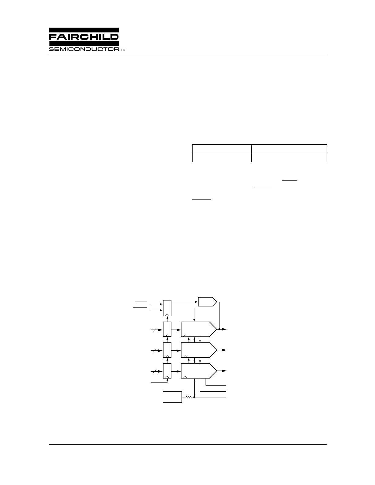
Block Diagram
Description
FMS3810/3815 products are low-cost triple D/A converters
that are tailored to fit graphics and video applications where
speed is critical. Two speed grades are available:
FMS3810 100 Ms/s
FMS3815 150 Ms/s
TTL-level inputs are converted to analog current outputs that
can drive 25–37.5 Ω loads corresponding to doubly-terminated
50–75 Ω loads. A sync current following SYNC input timing
is added to the I
inputs, setting I
BLANK = L. Although appropriate for many applications
the internal 1.235V reference voltage can be overridden by
the V
REF
input.
Few external components are required, just the current
reference resistor, current output load resistors, and
decoupling capacitors.
Package is a 48-lead LQFP. Fabrication technology is
CMOS. Performance is guaranteed from 0 to 70°C.
output. BLANK will override RGB
OG
, I
OG
OB
and I
currents to zero when
OR
SYNC
BLANK
G
7-0
B
7-0
R
7-0
CLOCK
SYNC
8
8
8
+1.235V
Ref
8 bit D/A
Converter
8 bit D/A
Converter
8 bit D/A
Converter
IO
G
IO
B
IO
R
COMP
R
REF
V
REF
REV. 1.08 12/21/00
Page 2
FMS3810/3815 PRODUCT SPECIFICATION
Functional Description
Within the FMS3810/3815 are three identical 10-bit D/A
converters, each with a current source output. External loads
are required to convert the current to voltage outputs. Data
inputs RGB
= H activates, sync current from I
signals.
Digital Inputs
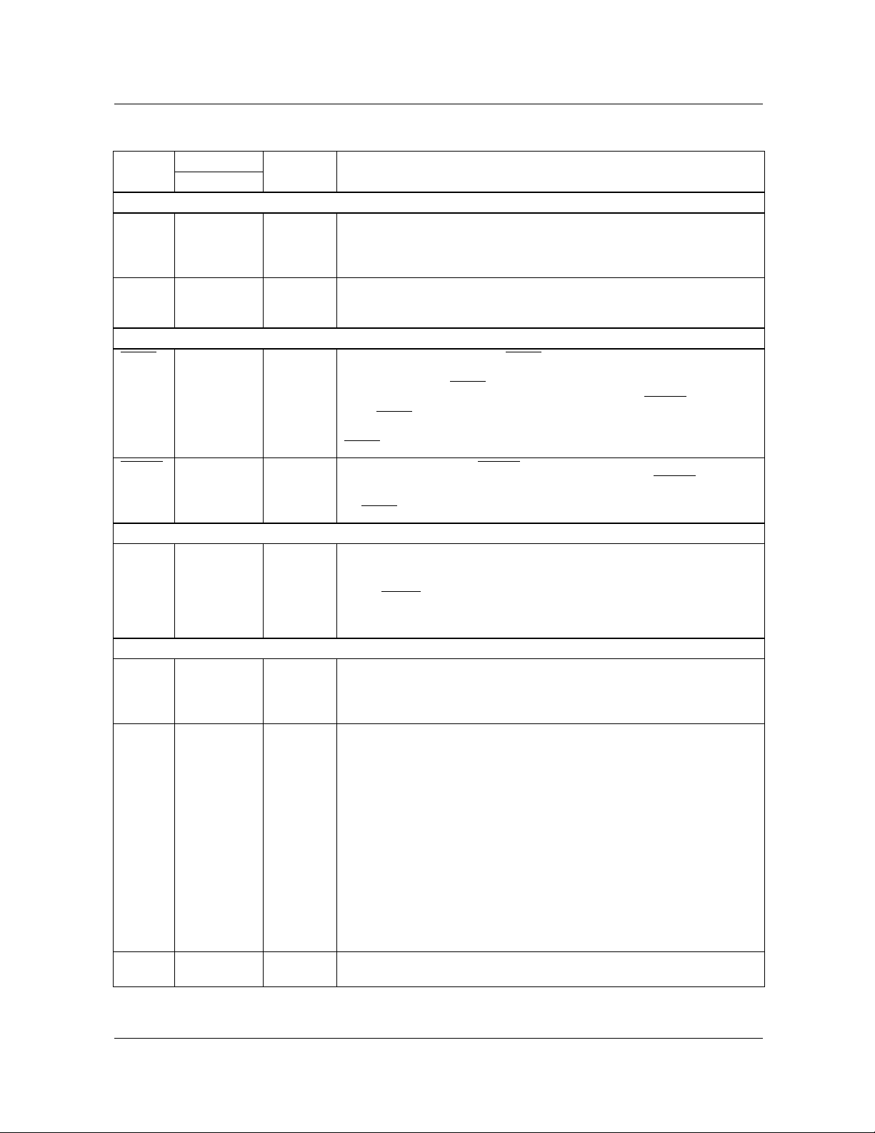
All digital inputs are TTL-compatible. Data is registered on
the rising edge of the CLK signal. Following one stage of
pipeline delay, the analog output changes t
edge of CLK.
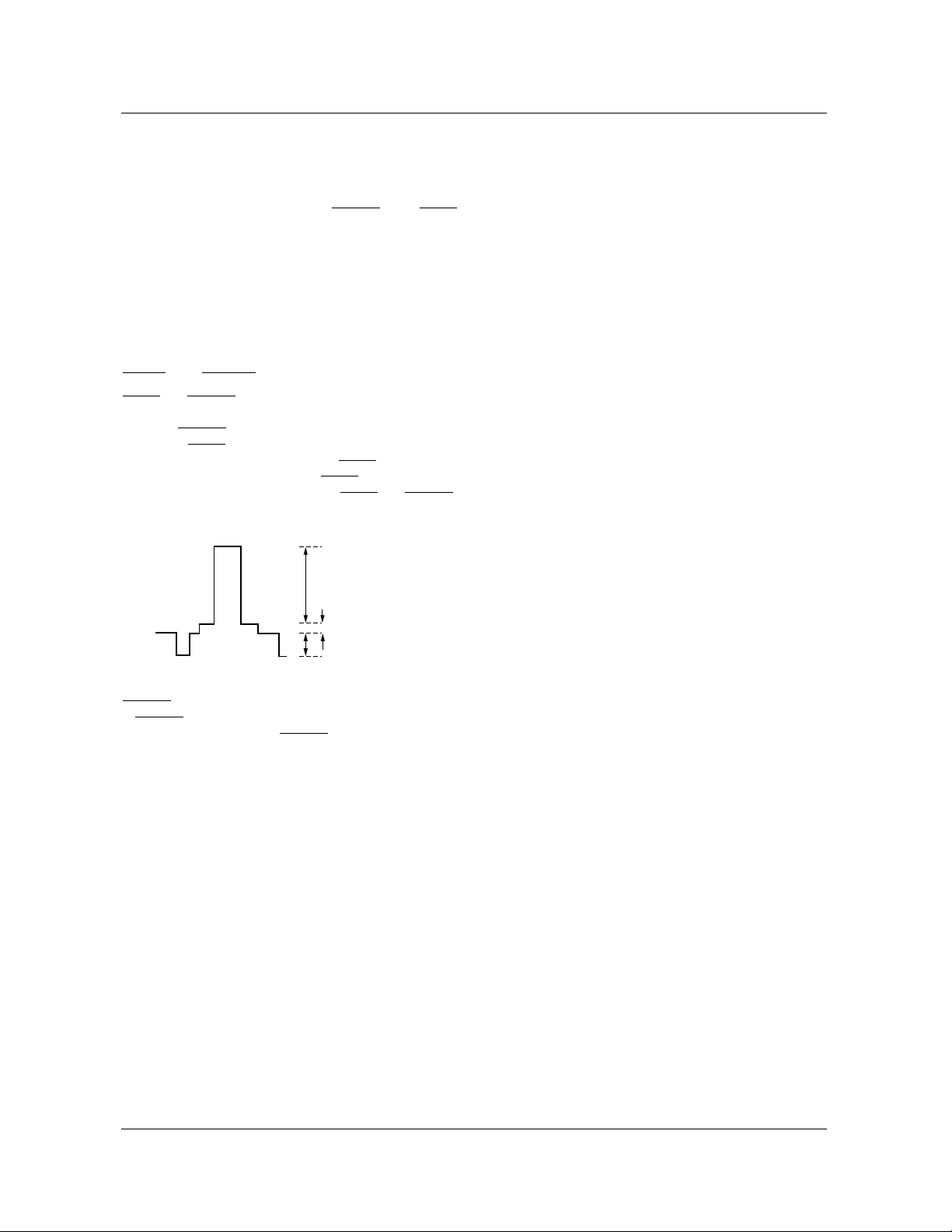
SYNC
SYNC and BLANK inputs control the output level (Figure 1
and Table 1) of the D/A converters during CRT retrace
intervals. BLANK forces the D/A outputs to the blanking
level while SYNC = L turns off a current source that is
connected to the green D/A converter. SYNC = H adds a 40
IRE sync pulse to the green output, SYNC = L sets the green
output to 0.0 Volts during the sync tip. SYNC and BLANK
are registered on the rising edge of CLK.
are overridden by the BLANK input. SYNC
7-0
for sync-on-green video
OS
DO
and BLANK
data: 660 mV max.
after the rising
D/A Outputs
Each D/A output is a current source. To obtain a voltage
output, a resistor must be connected to ground. Output
voltage depends upon this external resistor, the reference
voltage, and the value of the gain-setting resistor connected
between R
and GND.
REF
Normally, a source termination resistor of 75 Ohms is
connected between the D/A current output pin and GND
near the D/A converter. A 75 Ohm line may then be
connected with another 75 Ohm termination resistor at the
far end of the cable. This “double termination” presents the
D/A converter with a net resistive load of 37.5 Ohms.
The FMS3810/3815 may also be operated with a single 75
Ohm terminating resistor. To lower the output voltage swing
to the desired range, the nominal value of the resistor on
should be doubled.
R
REF
Voltage Reference
All three D/A converters are supplied with a common
voltage reference. Internal bandgap voltage reference voltage
is +1.235 Volts with a 3K Ω source resistance. An external
voltage reference may be connected to the V
overriding the internal voltage reference.
A 0.1µF capacitor must be connected between the COMP
pin and V
to stabilize internal bias circuitry and ensure
DD
low-noise operation.
REF
pin,
pedestal: 54 mV
sync: 286 mV
Figure 1. Nominal Output Levels
BLANK gates the D/A inputs and sets the pedestal voltage.
If BLANK = H, the D/A inputs are added to a pedestal which
offsets the current output. If BLANK = L, data inputs and the
pedestal are disabled.
Power and Ground
Required power is a single +5.0 Volt supply. To minimize
power supply induced noise, analog +5V should be
connected to V
capacitors placed adjacent to each V
High slew-rate of digital data makes capacitive coupling to
the outputs of any D/A converter a potential problem. Since
the digital signals contain high-frequency components of the
CLK signal, as well as the video output signal, the resulting
data feedthrough often looks like harmonic distortion or
reduced signal-to-noise performance. All ground pins should
be connected to a common solid ground plane for best
performance.
pins with 0.1 and 0.01 µF decoupling
DD
pin or pin pair.
DD
2
REV. 1.08 12/21/00
Page 3
PRODUCT SPECIFICATION FMS3810/3815
Table 1. Output Voltage versus Input Code, SYNC
V
= 1.235 V, R
REF
= 590 Ω , R
REF
= 37.5 Ω
L
and BLANK
Blue and Red Green
RGB7-0 (MSB…LSB)
SYNC BLANK V
OUT
SYNC BLANK V
1111 1111 X 1 0.714 1 1 1.000
1111 1111 X 1 0.714 0 1 0.714
1111 1110 X 1 0.711 1 1 0.997
1111 1101 X 1 0.709 1 1 0.995
•
•
•
•
•
•
•
•
•
•
•
•
0000 0000 X 1 0.385 1 1 0.671
1111 1111 X 1 0.383 1 1 0.669
•
•
•
•
•
•
•
•
•
•
•
•
0000 0010 X 1 0.059 1 1 0.345
0000 0001 X 1 0.057 1 1 0.343
0000 0000 X 1 0.054 1 1 0.340
0000 0000 X 1 0.054 0 1 0.054
XXXX XXXX X 0 0.000 1 0 0.286
XXXX XXXX X 0 0.000 0 0 0.000
XXXX XXXX X 1 valid 0 1 valid
OUT
•
•
•
•
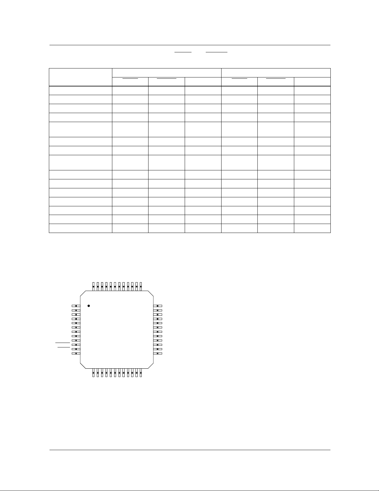
Pin Assignments
LQFP Package
GND
R7R6R5R4R3R2R
484746454443424140
G
G
G
G
G
G
G
G
DD
1
2
0
3
1
4
2
5
3
6
4
7
5
8
6
7
9
10
11
12
FMS3810/3815
131415161718192021
NC
GND
GND
GND
BLANK
SYNC
V
1
B0B1B2B3B4B6B
R0GND
GND
39
38
22
23
5
B
NC
37
R
36
35
34
33
32
31
30
29
28
27
26
25
24
7
NC
REF
V
REF
COMP
IO
R
IO
G
V
DD
V
DD
IO
B
GND
GND
CLOCK
NC
REV. 1.08 12/21/00
3
Page 4
)
FMS3810/3815 PRODUCT SPECIFICATION
Pin Descriptions
Pin
Name
Pin Number
Value Pin Function DescriptionLQFP
Clock and Pixel I/O
CLK 26 TTL
R
7-0
G
7-0
B
7-0
47-40
9-2
23-16
TTL
Controls
SYNC 11 TTL
BLANK 10 TTL
Video Outputs
IO
IO
IO
R
G
B
33
32
29
0.714 V
Clock Input. The clock input is TTL-compatible and all pixel data is
registered on the rising edge of CLK. It is recommended that CLK be
driven by a dedicated TTL buffer to avoid reflection induced jitter,
overshoot, and undershoot.
Red, Green, and Blue Pixel Inputs. TTL-compatible RGB digital inputs
are registered on the rising edge of CLK.
Sync Pulse Input. Bringing SYNC LOW, turns off a 40 IRE (7.62 mA)
current source which forms a sync pulse on any D/A converter output
connected to IO
. SYNC is registered on the rising edge of CLK along
S
with pixel data and has the same pipeline latency as BLANK and pixel
data. SYNC does not override any other data and should be used only
during the blanking interval. If the system does not require sync pulses,
SYNC and IO
should be connected to GND.
S
Blanking Input. When BLANK is LOW, pixel inputs are ignored and the
D/A converter outputs are driven to the blanking level. BLANK is
registered on the rising edge of CLK and has the same two-pipe latency
as SYNC and Data.
Red, Green, and Blue Current Outputs. Current source outputs can
p-p
drive RS-343A/SMPTE-170M compatible levels into doubly-terminated
75 Ohm lines. Sync pulses may be added to the green output.
When SYNC is HIGH, the current added to I
OG
is:
IO
= 3.64 (V
S
REF
/ R
REF
Voltage Reference
V
REF
35 +1.235 V Voltage Reference Input/Output. Internal 1.235V voltage reference is
available on this pin. An external +1.235 Volt reference may be applied to
this pin to override the internal reference. Decoupling V
to GND with
REF
a 0.1µF ceramic capacitor is required.
R
REF
36 590 Ω Current-setting Resistor. Full-scale output current of each D/A
converter is determined by the value of the resistor connected between
R
and GND. Nominal value of R
REF
R
REF
where I
= 9.1 (V
is the full-scale (white) output current (amps) from the
FS
REF
/I
)
FS
D/A converter (without sync). Sync is 0.4 I
is found from:
REF
.
FS
D/A full-scale (white) current may also be calculated from:
I
= V
FS
Where V
(ohms) on each D/A converter. V
/R
FS
L
is the white voltage level and R
FS
FS
is the total resistive load
L
is the blank to full-scale voltage.
COMP 34 0.1 µF Compensation Capacitor. A 0.1 µF ceramic capacitor should be
connected between COMP and V
to stabilize internal bias circuitry.
DD
4
REV. 1.08 12/21/00
Page 5

PRODUCT SPECIFICATION FMS3810/3815
Pin Descriptions
Pin
Pin Number
(continued)
Name
Power, Ground
V
DD
12, 30, 31 +5 V
GND 1, 14, 15, 27,
28, 38, 39, 48
NC 13, 24, 25, 37 —
Equivalent Circuits
Digital
Input
Value Pin Function DescriptionLQFP
0.0V
Power Supply.
Ground.
No Connect
V
DD
p
n
V
DD
np
V
DD
GND
Figure 1. Equivalent Digital Input Circuit
R
REF
V
REF
Figure 3. Equivalent Analog Input Circuit
OUT
GND
Figure 2. Equivalent Analog Output Circuit
V
DD
p
GND
p
27012B
REV. 1.08 12/21/00
5
Page 6

PRODUCT SPECIFICATION FMS3810/3815
Absolute Maximum Ratings
(beyond which the device may be damaged)
1
Parameter Min Typ Max Unit
Power Supply Voltage
V
(Measured to GND) -0.5 7.0 V
DD
Inputs
Applied Voltage (measured to GND)
Forced Current
3,4
2
-0.5 V
+ 0.5 V
DD
-10.0 10.0 mA
Outputs
Applied Voltage (measured to GND)
Forced Current
3,4
2
-0.5 V
+ 0.5 V
DD
-60.0 60.0 mA
Short Circuit Duration (single output in HIGH state to ground) unlimited sec.
Temperature
Operating, Ambient -20 110 °C
Junction 150 °C
Lead Soldering (10 seconds) 300 °C
Vapor Phase Soldering (1 minute) 220 °C
Storage -65 150 °C
Notes:
1. Functional operation under any of these conditions is NOT implied. Performance and reliability are guaranteed only if
Operating Conditions are not exceeded.
2. Applied voltage must be current limited to specified range.
3. Forcing voltage must be limited to specified range.
4. Current is specified as conventional current flowing into the device.
Operating Conditions
Parameter Min Nom Max Units
V
DD
f
S
t
PWH
t
PWL
t
W
t
s
t
h
V
REF
C
C
R
L
V
IH
V
IL
T
A
Power Supply Voltage 4.75 5.0 5.25 V
Conversion Rate FMS3810 100 Msps
FMS3815 150 Msps
CLK Pulsewidth, HIGH FMS3810 3.1 ns
FMS3815 2.5 ns
CLK Pulsewidth, LOW FMS3810 3.1 ns
FMS3815 2.5 ns
CLK Pulsewidth FMS3810 10 ns
FMS3815 6.6 ns
Input Data Setup Time 1.7 ns
Input Date Hold Time 0 ns
Reference Voltage, External 1.0 1.235 1.5 V
Compensation Capacitor 0.1 µF
Output Load 37.5 Ω
Input Voltage, Logic HIGH 2.0 V
DD
Input Voltage, Logic LOW GND 0.8 V
Ambient Temperature, Still Air 0 70 °C
V
REV. 1.08 12/21/00
6
Page 7

FMS3810/3815 PRODUCT SPECIFICATION
Electrical Characteristics
Parameter Conditions
I
DD
Power Supply Current
PD Total Power Dissipation
R
O
C
O
I
IH
I
IL
I
REF
V
REF
V
OC
C
DI
Notes:
1. Values shown in Typ column are typical for V
2. Minimum/Maximum values with V
3. V
Output Resistance 100 kΩ
Output Capacitance I
Input Current, HIGH VDD = Max, VIN = 2.4V -5 µA
Input Current, LOW VDD = Max, VIN = 0.4V 5 µA
V
Input Bias Current 0 ±100 µA
REF
Reference Voltage Output 1.235 V
Output Compliance Referred to V
Digital Input Capacitance 4 10 pF
= 1.235V, R
REF
LOAD
= 37.5Ω, R
2
DD
VDD = Max 125 mA
2
V
= Max 655 mW
DD
= 0mA 30 pF
OUT
= +5V and TA = 25°C
= Max and TA = Min
REF
DD
= 590Ω
3
DD
Min Typ
-0.4 0 +1.5 V
1
Max Units
Switching Characteristics
Parameter Conditions
t
D
t
SKEW
t
R
t
F
Notes:
1. Values shown in Typ column are typical for V
2. V
Clock to Output Delay VDD = Min 10 15 ns
Output Skew 1 2 ns
Output Risetime 10% to 90% of Full Scale 3 ns
Output Falltime 90% to 10% of Full Scale 3 ns
= +5V and TA = 25°C.
= 1.235V, R
REF
LOAD
= 37.5Ω, R
REF
DD
= 590Ω.
2
Min Typ
1
Max Units
System Performance Characteristics
Parameter Conditions
E
LI
E
LD
E
DM
Integral Linearity Error VDD, V
Differential Linearity Error VDD, V
DAC to DAC Matching VDD, V
2
= Nom ±0.2 ±0.3 %/FS
REF
= Nom ±0.2 ±0.3 %/FS
REF
= Nom 5 10 %
REF
Min Typ
PSRR Power Supply Rejection Ratio 0.05 %/%
Notes:
1. Values shown in Typ column are typical for V
2. V
= 1.235V, R
REF
LOAD
= 37.5Ω, R
REF
= 590Ω.
= +5V and TA = 25°C.
DD
7 REV. 1.08 12/21/00
1
Max Units
Page 8
FMS3810/3815 PRODUCT SPECIFICATION
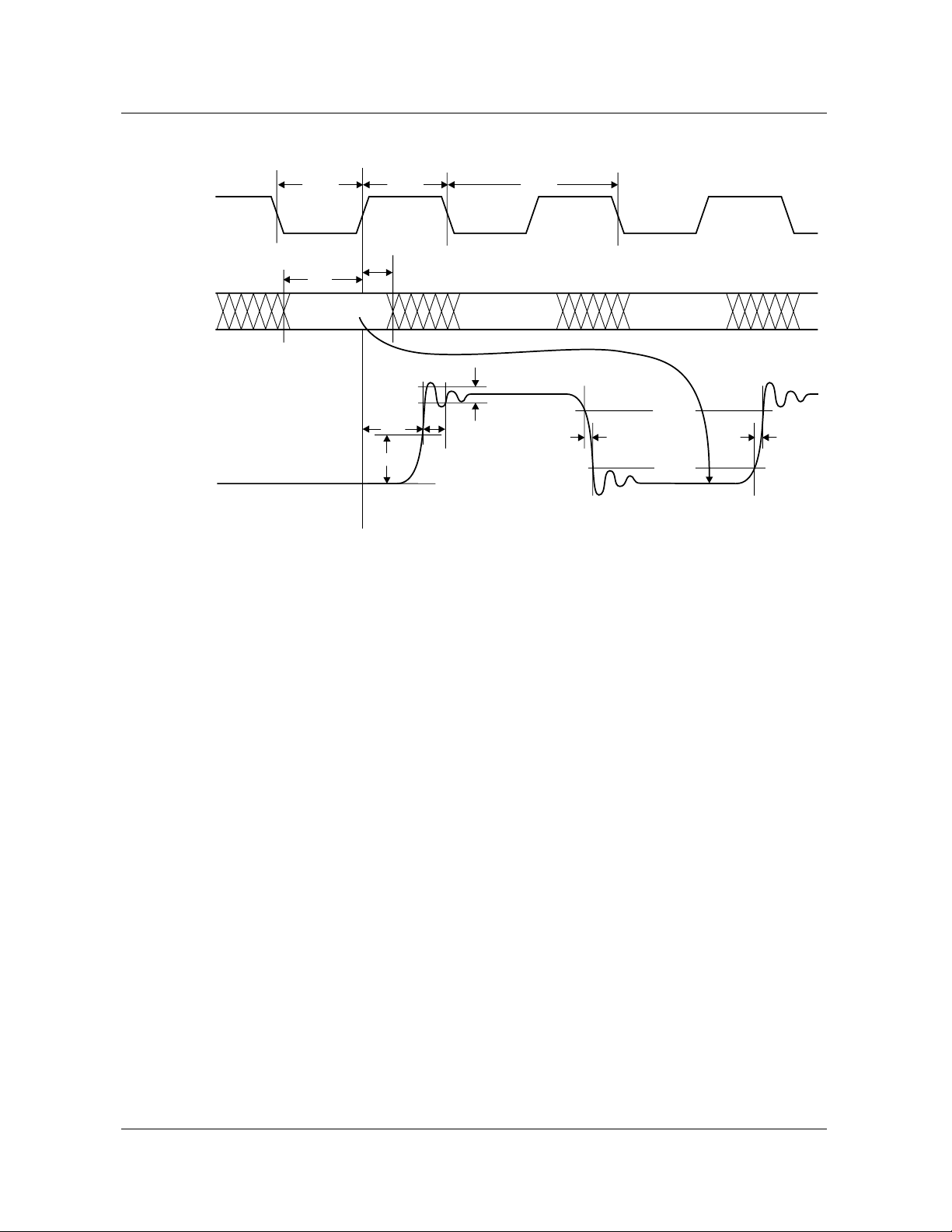
Timing Diagram
1/f
S
90%
t
F
10%
t
R
CLK
PIXEL DATA
& CONTROLS
OUTPUT
t
PWL
t
S
DataN DataN+1 DataN+2
50%
t
PWH
t
H
3%/FS
t
D
t
SET
Applications Information
Figure 4 illustrates a typical FMS3810/3815 interface
circuit. In this example, an optional 1.2 Volt bandgap
reference is connected to the V
internal voltage reference source.
Grounding
It is important that the FMS3810/3815 power supply is
well-regulated and free of high-frequency noise. Careful
power supply decoupling will ensure the highest quality
video signals at the output of the circuit. The FMS3810/3815
has separate analog and digital circuits. To keep digital
system noise from the D/A converter, it is recommended that
power supply voltages (VDD) come from the system analog
power source and all ground connections (GND) be made to
the analog ground plane. Power supply pins should be
individually decoupled at the pin.
Printed Circuit Board Layout
Designing with high-performance mixed-signal circuits
demands printed circuits with ground planes. Overall system
performance is strongly influenced by the board layout.
Capacitive coupling from digital to analog circuits may
result in poor D/A conversion. Consider the following
suggestions when doing the layout:
1. Keep the critical analog traces (V
IOS, IOR, IOG) as short as possible and as far as
possible from all digital signals. The FMS3810/3815
should be located near the board edge, close to the
analog output connectors.
output, overriding the
REF
, I
REF
REF
, COMP,
2. The power plane for the FMS3810/3815 should be
separate from that which supplies the digital circuitry.
A single power plane should be used for all of the VDD
pins. If the power supply for the FMS3810/3815 is the
same as that of the system's digital circuitry, power to
the FMS3810/3815 should be decoupled with 0.1µF and
0.01µF capacitors and isolated with a ferrite bead.
3. The ground plane should be solid, not cross-hatched.
Connections to the ground plane should have very short
leads.
4. If the digital power supply has a dedicated power plane
layer, it should not be placed under the FMS3810/3815,
the voltage reference, or the analog outputs. Capacitive
coupling of digital power supply noise from this layer to
the FMS3810/3815 and its related analog circuitry can
have an adverse effect on performance.
5. CLK should be handled carefully. Jitter and noise on
this clock will degrade performance. Terminate the
clock line carefully to eliminate overshoot and ringing.
8 REV. 1.08 12/21/00
Page 9

PRODUCT SPECIFICATION FMS3810/3815
+5V
10µF
0.1µF
RED PIXEL
INPUT
GREEN PIXEL
INPUT
BLUE PIXEL
INPUT
CLOCK
SYNC
BLANK
R
7-0
G
7-0
B
7-0
CLK
SYNC
BLANK
VDD
GND
FMS38XX
Triple 8-bit
D/A Converter
Figure 4. Typical Interface Circuit
Related Products
• FMS3110/3115 Triple 10-bit 250 Msps D/A Converters
• FMS9884A 3 x 8 bit 140 Ms/s A/D Converter
IO
IO
IO
COMP
V
REF
R
REF
Red
R
75Ω
G
75Ω
B
ZO=75Ω
Green w/Sync
ZO=75Ω
Blue
Z
O
=75Ω
75Ω
75Ω
75Ω
75Ω
+5V
0.1µF
3.3kΩ (not required without
external reference)
0.1µF
590Ω
LM185-1.2
(Optional)
REV. 1.08 12/21/00 9
Page 10

FMS3810/3815 PRODUCT SPECIFICATION
Mechanical Dimensions
48-Lead LQFP Package
Symbol
A .055 .063 1.40 1.60
A1 .001 .005 .05 .15
A2 .053 1.35
B .006 .010 .17 .27
D/E
D1/E1
e
L .017 .029 .45 .75 6
N48 48
ND
α 0° 7° 0° 7°
ccc .004 0.08
E
Inches
Min. Max. Min. Max.
.057 1.45
.346 .362 8.8 9.2
.268 .284 6.8 7.2
.019 BSC
12 12
E1
Millimeters
.50 BSC
D
D1
PIN 1
IDENTIFIER
Notes
Notes:
All dimensions and tolerances conform to ANSI Y14.5M-1982.
1.
Dimensions "D1" and "E1" do not include mold protrusion.
2.
Allowable protrusion is 0.25mm per side. D1 and E1 are maximum
plastic body size dimensions including mold mismatch.
Pin 1 identifier is optional.
3.
7
8
2
4
5
Dimension ND: Number of terminals.
4.
Dimension ND: Number of terminals per package edge.
5.
"L" is the length of terminal for soldering to a substrate.
6.
Dimension "B" does not include dambar protrusion. Allowable
7.
dambar protrusion shall not cause the lead width to exceed the
maximum B dimension by more than 0.08mm. Dambar can not be
located on the lower radius or the foot. Minimum space between
protrusion and an adjacent lead is 0.07mm for 0.4mm and 0.5mm
pitch packages.
8.
To be determined at seating place —C—
e
C
L
0.063" Ref (1.60mm)
See Lead Detail
A2
A
B
A1
Seating Plane
Base Plane
-C-
LEAD COPLANARITY
ccc
C
α
10 REV. 1.08 12/21/00
Page 11

FMS3810/3815 PRODUCT SPECIFICATION
Ordering Information
Product Number
Conversion
Rate Temperature Range Screening Package
Package
Marking
FMS3810KRC 100 Ms/s TA = 0°C to 70°C Commercial 48-Lead LQFP 3810KRC
FMS3815KRC 150 Ms/s TA = 0°C to 70°C Commercial 48-Lead LQFP 3815KRC
DISCLAIMER
FAIRCHILD SEMICONDUCTOR RESERVES THE RIGHT TO MAKE CHANGES WITHOUT FURTHER NOTICE TO
ANY PRODUCTS HEREIN TO IMPROVE RELIABILITY, FUNCTION OR DESIGN. FAIRCHILD DOES NOT ASSUME
ANY LIABILITY ARISING OUT OF THE APPLICATION OR USE OF ANY PRODUCT OR CIRCUIT DESCRIBED HEREIN;
NEITHER DOES IT CONVEY ANY LICENSE UNDER ITS PATENT RIGHTS, NOR THE RIGHTS OF OTHERS.
LIFE SUPPORT POLICY
FAIRCHILD’S PRODUCTS ARE NOT AUTHORIZED FOR USE AS CRITICAL COMPONENTS IN LIFE SUPPORT DEVICES
OR SYSTEMS WITHOUT THE EXPRESS WRITTEN APPROVAL OF THE PRESIDENT OF FAIRCHILD SEMICONDUCTOR
CORPORATION. As used herein:
1. Life support devices or systems are devices or systems
which, (a) are intended for surgical implant into the body,
or (b) support or sustain life, and (c) whose failure to
perform when properly used in accordance with
instructions for use provided in the labeling, can be
reasonably expected to result in a significant injury of the
user.
www.fairchildsemi.com
2. A critical component in any component of a life support
device or system whose failure to perform can be
reasonably expected to cause the failure of the life support
device or system, or to affect its safety or effectiveness.
12/21/00 0.0m 003
2000 Fairchild Semiconductor Corporation
Stock#DS30003810
 Loading...