

Page 1
FMMT459
450V SILICON NPN HIGH VOLTAGE SWITCHING TRANSISTOR
SUMMARY
V
=450V; VCE(sat) = 100mV; IC= 150mA
CEO
DESCRIPTION
This new high voltage tranistor provides users with very effiecient
performance combining low V
losses at 450V operation, making it ideal for use in high efficiency Telecom
and protected line switching applications.
FEATURES
Low Saturation Voltage - 90mV @ 50mA
•
Hfe Min 50 @ 30 mA
•
=150mA Continuous
I
•
C
• SOT23 package with Ptot 625mW
• Specification can be supplied in larger package outlines
APPLICATIONS
• Electronic test equipment
• Off line switching circuits
• Piezo Actuators.
•
RCD circuits.
ORDERING INFORMATION
DEVICE REEL SIZE
(inches)
(sat) and Hfe to give extremely low on state
CE
TAPE WIDTH
(mm)
QUANTITY
PER REEL
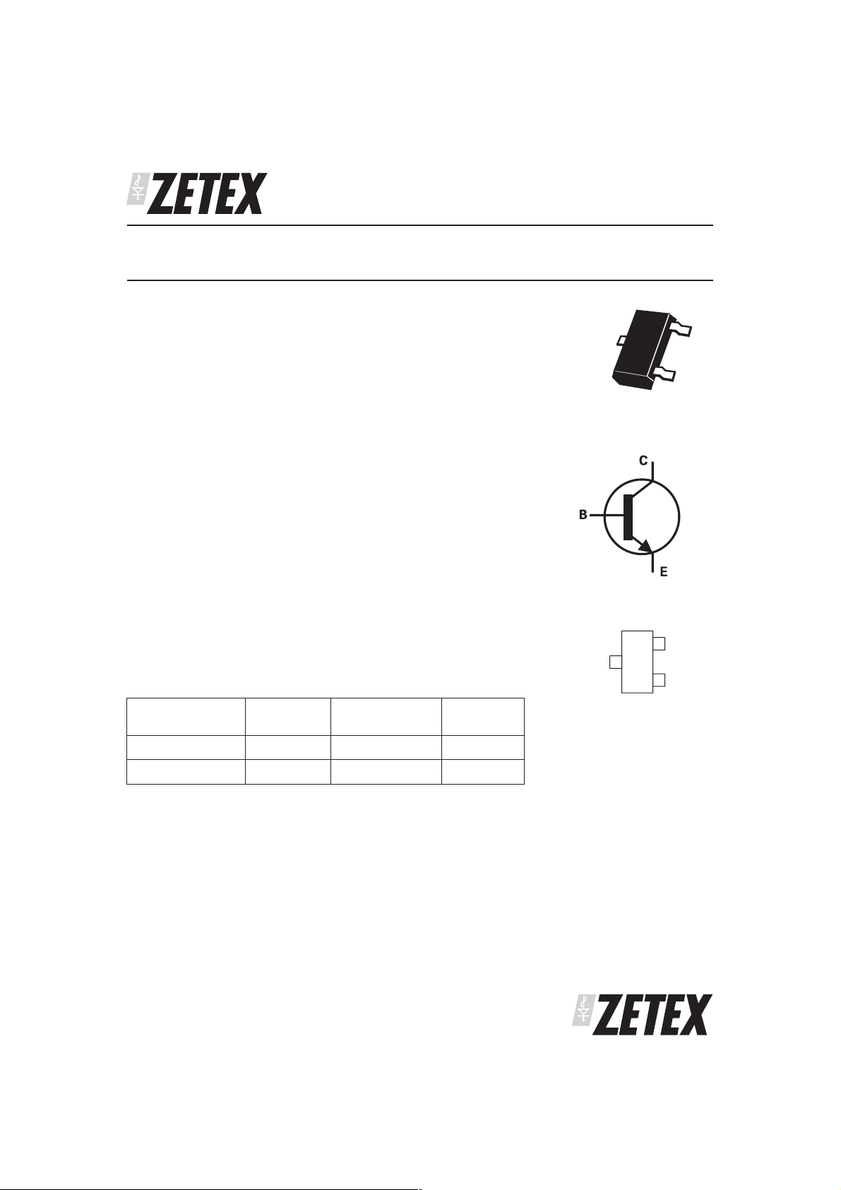
SOT23
C
Top View
E
B
FMMT459TA 7 8mm embossed 3000 units
FMMT459TC
DEVICE MARKING
459
ISSUE 2 - DECEMBER 2001
13 8mm embossed 10000 units
1
Page 2
FMMT459
ABSOLUTE MAXIMUM RATINGS.
PARAMETER SYMBOL LIMIT UNIT
Collector-Base Voltage V
Collector-Emitter Voltage V
Emitter-Base Voltage V
Peak Pulse Current I
Continuous Collector Current I
Base Current I
Power Dissipation at TA=25°C (a)
Linear Derating Factor
Power Dissipation at TA=25°C (b)
Linear Derating Factor
Operating and Storage Temperature Range T
CM
C
B
P
P
CBO
CEO
EBO
D
D
j:Tstg
500 V
450 V
5V
500 mA
150 mA
200 mA
625
5
806
6.4
mW
mW/°C
mW
mW/°C
-55 to +150 °C
THERMAL RESISTANCE
PARAMETER SYMBOL VALUE UNIT
Junction to Ambient (a) R
Junction to Ambient (b) R
θJA
θJA
NOTES
(a) For a device surface mounted on 25mm x 25mm FR4 PCB with high coverage of single sided 1oz copper,
in still air conditions
(b) For a device surface mounted on FR4 PCB measured at t⭐5 secs.
2
200 °C/W
155 °C/W
ISSUE 2 - DECEMBER 2001
Page 3

FMMT459
ELECTRICAL CHARACTERISTICS (at T
= 25°C unless otherwise stated)
amb
PARAMETER SYMBOL MIN. TYP. MAX. UNIT CONDITIONS
Collector-Base
Breakdown Voltage
Collector-Emitter
Breakdown Voltage
Emitter-Base
Breakdown Voltage
V
(BR)CBO
V
CEO(sus)
V
(BR)EBO
Collector Cut-Off
Current
Emitter Cut-Off Current I
Collector Emitter
Cut-Off Current
Collector Emitter
Saturation Voltage
Base-Emitter Saturation
Voltage
Base-Emitter Turn-On
V
CE(sat)
V
BE(sat)
V
Voltage
Static Forward Current
Transfer Ratio
Transition Frequency f
Output Capacitance C
Turn-On Time t
Turn-Off Time t
I
CBO
EBO
I
CES
BE(on)
H
FE
T
OBO
(on)
(off)
500 700 V
I
= 100µA
C
450 500 V IC= 10mA*
58 V
I
= 100µA
E
100 nA VCB= 450V
100 nA VEB=5V
100 nA VCE= 450V
60
70
75
90
mVmVIC= 20mA, IB= 2mA*
= 50mA, IB= 6mA*
I
C
.76 .9 V IC= 50mA, IB= 5mA*
.71 .9 V IC= 50mA, VCE= 10V*
50 120
70
IC= 30mA, VCE= 10V*
= 50mA, VCE= 10V*
I
C
50 MHz IC= 10mA, VCE= 20V
F = 20MH
5
FVCB= 20V, f = 1MH
P
Z
113 ns IC= 50mA, VC= 100V
= 5mA, IB2= 10mA
I
B1
3450 ns IC= 50mA, VC= 100V
= 5mA, IB2= 10mA
I
B1
Z
*Measured under plused conditions. Pulse width = 300µs. Dury cycle <2%
NB. For high voltage applications, the appropriate industry sector guidelines should be
considered with regards to voltage spacing between Terminals.
ISSUE 2 - DECEMBER 2001
3
Page 4

FMMT459
ELECTRICAL CHARACTERISTICS
1
Tamb=25°C
IC/IB=50
(V)
100m
CE(SAT)
V
10m
1m 10m 100m
ICColl ector Curr ent (A)
1.2
1.0
0.8
0.6
0.4
NormalisedGain
0.2
0.0
100°C
25°C
-55°C
1m 10m 100m
IC/IB=20
V
CE(SAT )vIC
ICColl ector Curr ent (A)
hFEvI
C
IC/IB=10
VCE=10V
210
180
150
120
90
60
30
0
0.40
IC/IB=20
0.35
0.30
0.25
(V)
0.20
0.15
CE(SAT)
V
0.10
0.05
1m 10m 100m
ICCollector Current (A)
1.0
IC/IB=20
)
0.8
FE
-55°C
100°C
25°C
V
CE(SAT )vIC
(V)
0.6
BE(SAT)
V
0.4
Typical Gain (h
1m 10m 100m
25°C
100°C
ICCollector Current (A)
V
BE(SAT )vIC
-55°C
1.0
VCE=10V
0.8
(V)
0.6
BE(ON)
V
0.4
-55°C
25°C
100°C
1m 10m 100m
ICColl ector Curr ent (A)
V
BE( ON)vIC
ISSUE 2 - DECEMBER 2001
4
Page 5

THERMAL CHARACTERISTICS
FMMT459
1
100m
DC
1s
10m
Col lec tor Current ( A)
C
I
1m
100m 1 10 100
100ms
Single Pulse T
10ms
amb
=25°C
1ms
100µs
VCECollector-Emitter Voltage (V)
Safe Operating Area
200
150
D=0. 5
100
D=0. 2
50
0
Thermal Resistance (°C/W)
100µ 1m 10m 100m 1 10 100 1k
Single Pulse
D=0.05
D=0. 1
Pulse Widt h (s)
Transient Thermal Impedance
0.7
0.6
0.5
0.4
0.3
0.2
0.1
0.0
Max Power Dissipat ion (W)
0 20 40 60 80 100 120 140 160
Temperature (°C)
Derating Curve
ISSUE 2 - DECEMBER 2001
5
Page 6

FMMT459
PACKAGE DIMENSIONS PAD LAYOUT DETAILS
N
DIM Millimetres Inches
Min Max Min Max
A 2.67 3.05 0.105 0.120
B 1.20 1.40 0.047 0.055
C – 1.10 – 0.043
D 0.37 0.53 0.0145 0.021
F 0.085 0.15 0.0033 0.0059
G NOM 1.9 NOM 0.075
K 0.01 0.10 0.0004 0.004
L 2.10 2.50 0.0825 0.0985
NOM 0.95 NOM 0.037
N
© Zetex plc 2001
Zetex plc
Fields New Road
Chadderton
Oldham, OL9 8NP
United Kingdom
Telephone (44) 161 622 4422
Fax: (44) 161 622 4420
These offices are supported by agents and distributors in major countries world-wide.
This publicationis issued toprovide outline informationonly which (unlessagreed by theCompany in writing)may not beused,appliedor reproduced
for any purposeorformpart of anyorderor contract orberegardedas a representationrelatingtothe products orservicesconcerned. The Company
reserves the right to alter without notice the specification, design, price or conditions of supply of any product or service.
For the latest product information, log on to
Zetex GmbH
Streitfeldstraße 19
D-81673 München
Germany
Telefon: (49) 89 45 49 49 0
Fax: (49) 89 45 49 49 49
www.zetex.com
Zetex Inc
700 Veterans Memorial Hwy
Hauppauge, NY11788
USA
Telephone: (631) 360 2222
Fax: (631) 360 8222
Zetex (Asia) Ltd
3701-04 Metroplaza, Tower 1
Hing Fong Road
Kwai Fong
Hong Kong
Telephone: (852) 26100 611
Fax: (852) 24250 494
ISSUE 2 - DECEMBER 2001
6
 Loading...