

Page 1
Advance Technical Information
Trench Gate HiperFET
FMM60-02TF
N-Channel Power MOSFET
3
3
5
5
4
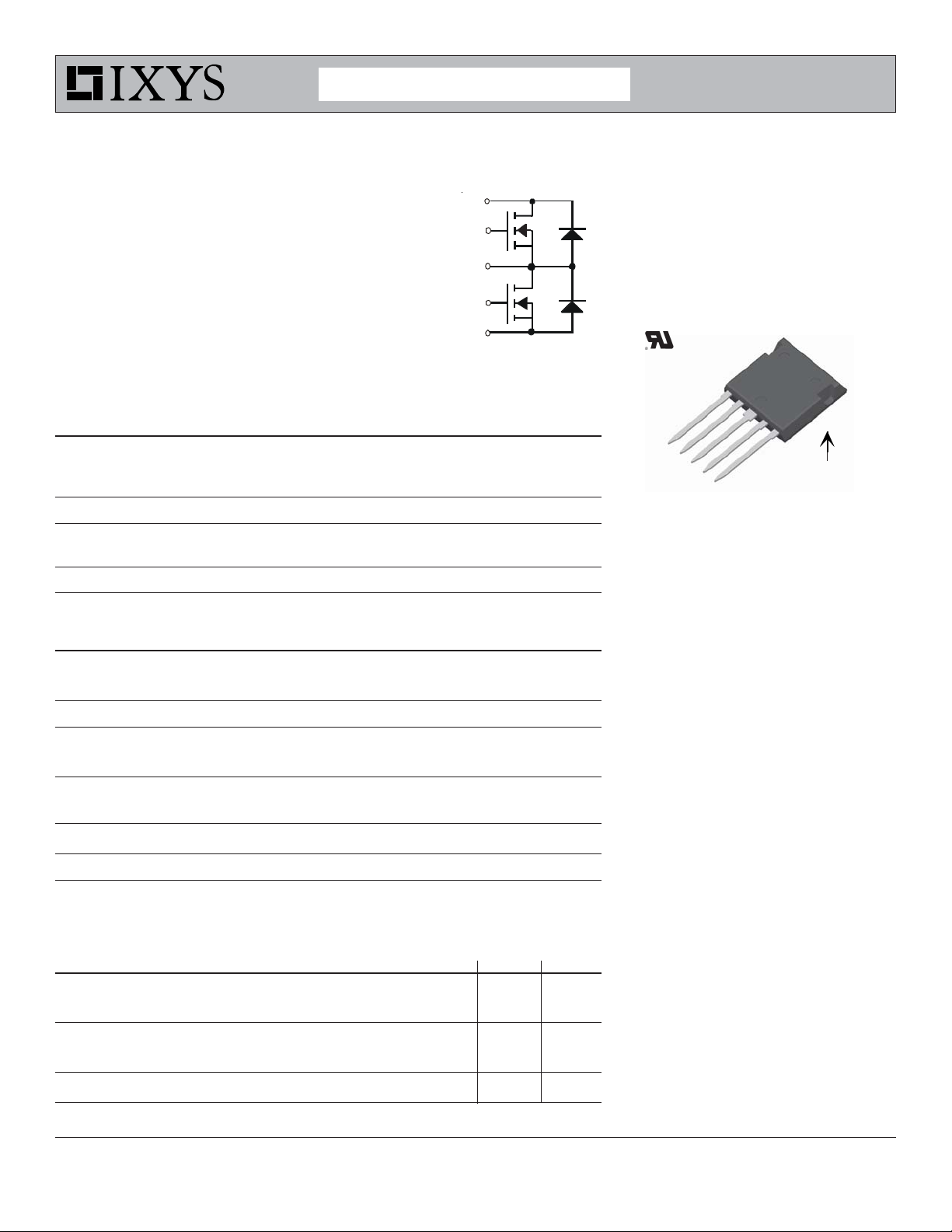
Phase Leg Topology
Symbol Test Conditions Maximum Ratings
T
J
T
JM
T
stg
V
ISOLD
T
L
T
SOLD
F
C
Symbol Test Conditions Maximum Ratings
V
DSS
V
DGR
V
GSM
I
D25
I
DM
I
A
E
AS
dV/dt IS≤ IDM, VDD ≤ V
PD TC= 25°C 125 W
50/60HZ, RMS, t = 1min, leads-to-tab 2500 ~V
1.6mm (0.062 in.) from case for 10s 300 °C
Plastic body for 10s 260 °C
Mounting force 20..120 / 4.5..27 N/lb.
TJ= 25°C to 150°C 200 V
TJ= 25°C to 150°C, RGS = 1MΩ 200 V
Transient ± 30 V
TC= 25°C 33 A
TC= 25°C, pulse width limited by T
TC= 25°C 5 A
TC= 25°C 1 J
≤ 150°C 10 V/ns
DSS,TJ
-55 ... +150 °C
150 °C
-55 ... +150 °C
JM
150 A
4
1
1
2
2
T1
T2
V
DSS
I
D25
R
DS(on)
t
rr(typ)
ISOPLUS i4-Pak
= 200V
= 33A
≤≤
≤ 40m
≤≤
= 82ns
TM
ΩΩ
Ω
ΩΩ
1
Isolated Tab
5
Features
z
Silicon chip on Direct-Copper Bond
(DCB) substrate
- UL recognized package
- Isolated mounting surface
- 2500V electrical isolation
z
Avalanche rated
z
Low Q
z
z
Advantages
z
z
z
z
z
G
Low Drain-to-Tab capacitance
Low package inductance
Low gate drive requirement
High power density
Fast intrinsic rectifier
Low drain to ground capacitance
Fast switching
Symbol Test Conditions Characteristic Values
Min. Typ. Max.
C
P
pins and mounting tab in the case
dS ,d
A
dS ,d
A
Weight 9 g
© 2008 IXYS CORPORATION, All rights reserved
Coupling capacitance between shorted 40 pF
pin - pin 1.7 mm
pin - backside metal 5.5 mm
Applications
z
DC and AC motor drives
z
UPS, solar and wind power inverters
z
Synchronous rectifiers
z
Multi-phase DC to DC converters
z
Industrial battery chargers
z
Switching power supplies
DS100048(09/08)
Page 2
FMM60-02TF
Symbol Test Conditions2 Characteristic Values
(TJ = 25°C unless otherwise specified) Min. Typ. Max.
BV
V
I
GSS
I
DSS
DSS
GS(th)
VGS= 0V, ID = 250μA 200 V
VDS= VGS, ID = 250μA 2.5 4.5 V
VGS= ±20 V, VDS = 0V ± 200 nA
VDS= V
DSS
5 μA
VGS = 0V TJ = 125°C 250 μA
R
g
C
C
C
t
d(on)
t
r
t
d(off)
t
f
Q
Q
Q
R
R
DS(on)
fs
iss
oss
rss
g(on)
gs
gd
thJC
thCS
VGS= 10V, ID = 30A, Note 1 32 40 mΩ
V
= 10V, ID = 60A, Note 1 40 62 S
DS
3700 pF
VGS = 0V, VDS = 25 V, f = 1 MHz 520 pF
37 pF
Resistive Switching Times 39 ns
VGS = 10V, VDS = 0.5 z V
, ID = 30A 46 ns
DSS
RG = 5Ω (External) 75 ns
42 ns
90 nC
VGS= 10V, VDS = 0.5 z V
, ID = 30A 33 nC
DSS
21 nC
1.0 °C/W
0.15 °C/W
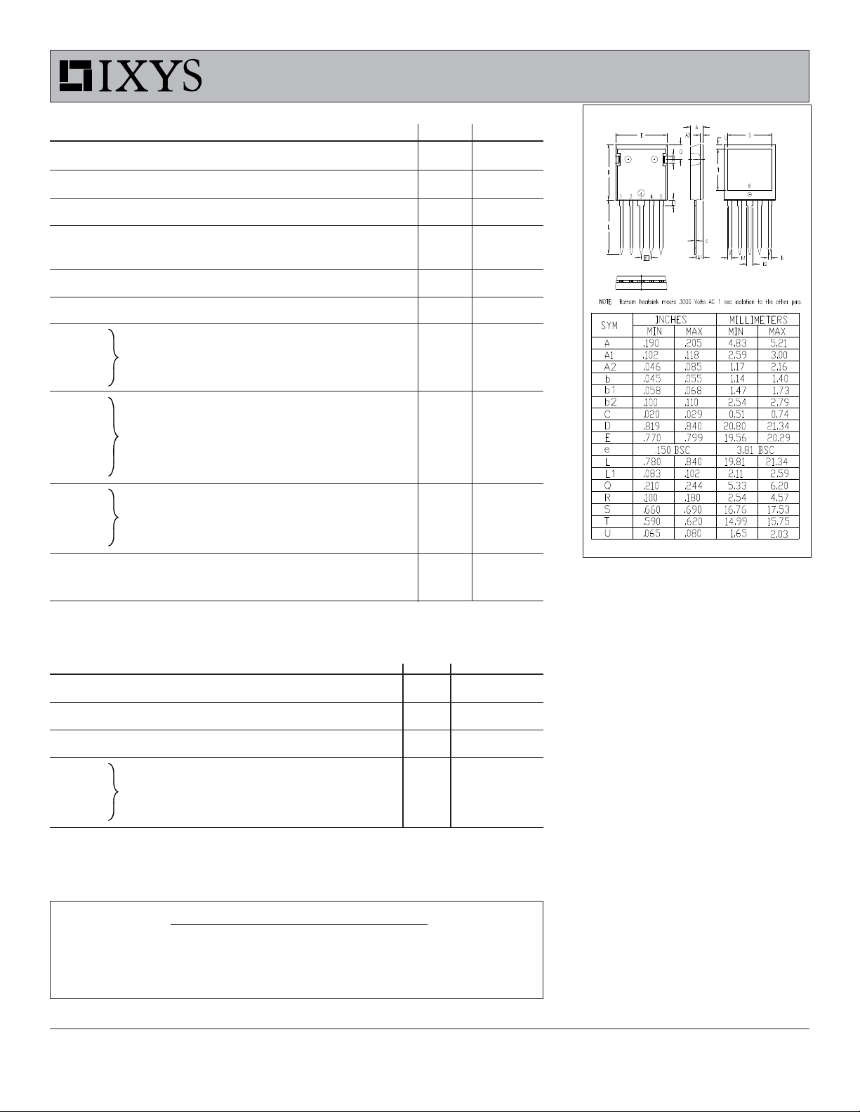
ISOPLUS i4-PakTM Outline
Ref: IXYS CO 0077 R0
Source-Drain Diode Characteristic Values
TJ = 25°C unless otherwise specified)
Symbol Test Conditions
I
S
I
SM
V
SD
t
rr
I
RM
Q
RM
VGS = 0V 33 A
Repetitive, pulse width limited by T
IF = 60A, VGS = 0V, Note 1 1.5 V
82 ns
IF = 25A, -di/dt = 100A/μs
15.3 A
V
= 100V, VGS = 0V
R
0.63 μC
3
Min. Typ. Max.
JM
150 A
Note 1: Pulse test, t ≤ 300μs, duty cycle, d ≤ 2 %.
ADVANCE TECHNICAL INFORMATION
The product presented herein is under development. The Technical Specifications offered are
derived from a subjective evaluation of the design, based upon prior knowledge and experience,
and constitute a "considered reflection" of the anticipated objective result. IXYS reserves the right
to change limits, test conditions, and dimensions without notice.
IXYS reserves the right to change limits, test conditions, and dimensions.
IXYS MOSFETs and IGBTs are covered 4,835,592 4,931,844 5,049,961 5,237,481 6,162,665 6,404,065 B1 6,683,344 6,727,585 7,005,734 B2 7,157,338B2
by one or more of the following U.S. patents: 4,850,072 5,017,508 5,063,307 5,381,025 6,259,123 B1 6,534,343 6,710,405 B2 6,759,692 7,063,975 B2
4,881,106 5,034,796 5,187,117 5,486,715 6,306,728 B1 6,583,505 6,710,463 6,771,478 B2 7,071,537
 Loading...