

Page 1
FMG1G75US60H
FMG1G75US60H
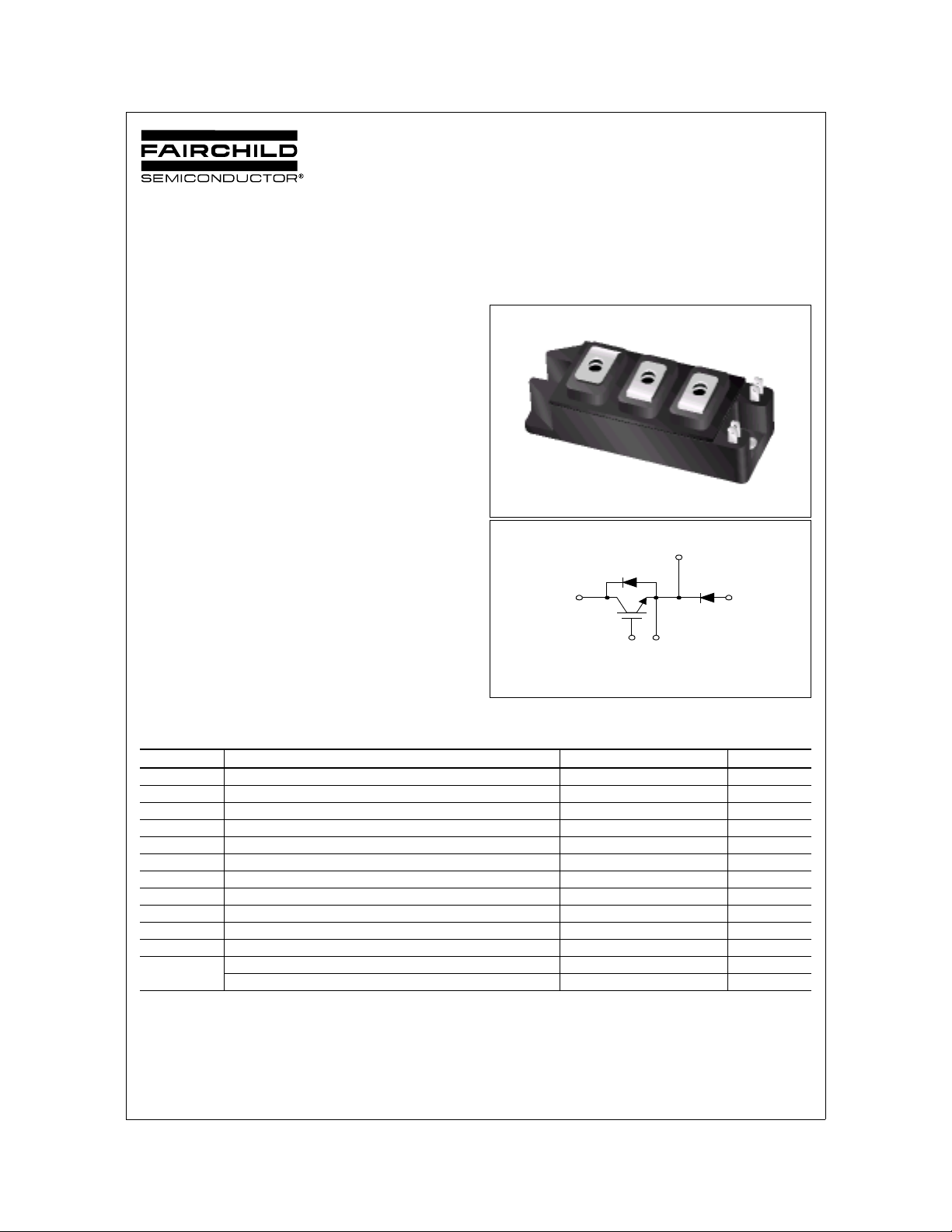
Molding Type Module
General Description
Fairchild’s Insulated Gate Bipolar Transistor (IGBT) power
modules provide low conduction and switching losses as
well as short circuit ruggedness. They are designed for
applications such as motor control, uninterrupted power
supplies (UPS) and general inverters wher e short circuit
ruggedness is a required feature.
Features
• UL Certified No. E209204
• Short Circuit rated 10us @ T
• High Speed Switching
• Low Saturation Voltage : V
• High Input Impedance
• Fast & Soft Anti-Parallel FWD
Application
• AC & DC Motor Controls
• General Purpose Inverters
• Robotics
• Servo Controls
•UPS
= 100°C, VGE = 15V
C
= 2.2 V @ IC = 75A
CE(sat)
Package Code : 7PM-GA
E1/C2
C1
G1
E1
Internal Circuit Diagram
IGBT
E2
Absolute Maximum Ratings T
Symbol Description FMG1G75US60H Units
V
CES
V
GES
I
C
I
CM (1)
I
F
I
FM
T
SC
P
D
Operating Junction Temperature -40 to +150 °C
T
J
T
stg
V
iso
Mounting
Torque
Notes :
(1) Repetitive rating : Pulse width limited by max. junction temperature
©2002 Fairchild Semiconductor Corporation FMG1G75US60H Rev. A
Collector-Emitter Voltage 600 V
Gate-Emitter Voltage ± 20 V
Collector Curent @ TC = 25°C75 A
Pulsed Collector Current 150 A
Diode Continuous Forward Current @ TC = 100°C75 A
Diode Maximum Forward Current 150 A
Short Circuit Withstand Time @ TC = 100°C10 us
Maximum Power Dissipation @ TC = 25°C 310 W
Storage Temperature Range -40 to +125 °C
Isolation Voltage @ AC 1minute 2500 V
Power Terminals Screw : M5 2.0 N.m
Mounting Screw : M5 2.0 N.m
= 25°C unless otherwise noted
C
Page 2

FMG1G75US60H
Electrical Characteristics of IGBT T
= 25°C unless otherwise noted
C
Symbol Parameter Test Conditions Min. Typ. Max. Units
Off Characteristics
BV
∆B
∆T
I
CES
I
GES
CES
VCES
J
Collector-Emitter Breakdown Voltage VGE = 0V, IC = 250uA 600 -- -- V
/
Temperature Coeff. of Breakdown
Voltage
Collector Cut-Off Current VCE = V
G-E Leakage Current VGE = V
V
= 0V, IC = 1mA -- 0.6 -- V/°C
GE
, VGE = 0V -- -- 250 uA
CES
, VCE = 0V -- -- ± 100 nA
GES
On Characteristics
V
GE(th)
V
CE(sat)
G-E Threshold Voltage VGE = 0V, IC = 75mA 5.0 6.0 8.5 V
Collector to Emitter
Saturation Voltage
= 75A, VGE = 15V
I
C
-- 2.2 2.8 V
Dynamic Characteristics
C
ies
C
oes
C
res
Input Capacitance
Output Capacitance -- 672 -- pF
Reverse Transfer Capacitance -- 180 -- pF
= 30V, VGE = 0V,
V
CE
f = 1MHz
-- 7056 -- pF
Switching Characteristics
t
d(on)
t
r
t
d(off)
t
f
E
on
E
off
Total Switching Loss -- 3.1 -- mJ
E
ts
t
d(on)
t
r
t
d(off)
t
f
E
on
E
off
E
Total Switching Loss -- 4.6 -- mJ
ts
T
sc
Q
g
Q
ge
Q
gc
Turn-On Delay Time
Rise Time -- 40 -- ns
Turn-Off Delay Time -- 70 -- ns
Fall Time -- 110 200 ns
Turn-On Switching Loss -- 1.4 -- mJ
= 300 V, IC = 75A,
V
CC
= 3.3Ω, V
R
G
GE
Inductive Load, T
= 15V
= 25°C
C
Turn-Off Switching Loss -- 1.7 -- mJ
Turn-On Delay Time
Rise Time -- 50 -- ns
Turn-Off Delay Time -- 80 -- ns
Fall Time -- 250 -- ns
Turn-On Switching Loss -- 1.6 -- mJ
= 300 V, IC = 75A,
V
CC
= 3.3Ω, V
R
G
Inductive Load, T
GE
= 15V
= 125°C
C
Turn-Off Switching Loss -- 3.0 -- mJ
= 300 V, V
V
Short Circuit Withstand Time
Total Gate Charge
Gate-Emitter Charge -- 62 -- nC
Gate-Collector Charge -- 130 -- nC
CC
@
TC = 100°C
= 300 V, IC = 75A,
V
CE
= 15V
V
GE
GE
= 15V
-- 20 -- ns
-- 20 -- ns
10 -- -- us
-- 310 350 nC
©2002 Fairchild Semiconductor Corporation FMG1G75US60H Rev. A
Page 3
FMG1G75US60H
Electrical Characteristics of DIODE T
= 25°C unless otherwise noted
C
Symbol Parameter Test Conditions Min. Typ. Max. Units
T
= 25°C
V
FM
t
rr
I
rr
Q
rr
Diode Forward Voltage IF = 75A
Diode Reverse Recovery Time
I
Diode Peak Reverse Recovery
Current
= 75A
F
di / dt = 150 A/us
Diode Reverse Recovery Charge
C
T
C
T
C
T
C
T
C
T
C
T
C
T
C
= 100°C
= 25°C
= 100°C
= 25°C
= 100°C
= 25°C
= 100°C
-- 1.9 2.8
-- 1.8 --
-- 90 130
-- 130 --
-- 7 9
-- 10 --
-- 315 590
-- 650 --
Thermal Characteristics
Symbol Parameter Typ. Max. Units
R
θJC
R
θJC
R
θCS
Weight Weight of Module -- 190 g
Junction-to-Case (IGBT Part, per 1/2 Module) -- 0.4 °C/W
Junction-to-Case (DIODE Part, per 1/2 Module) -- 0.9 °C/W
Case-to-Sink (Conductive grease applied) 0. 05 -- °C/W
V
ns
A
nC
©2002 Fairchild Semiconductor Corporation FMG1G75US60H Rev. A
Page 4

FMG1G75US60H
200
Common Emitter
180
TC = 25
160
140
[A]
C
120
100
80
60
Collector Cu rrent, I
40
20
0
02468
20V
℃
15V
12V
Vge = 10V
Collector - Emitter Voltage, VCE [V]
200
Common E mitter
V
= 15V
GE
T
= 25℃
C
160
= 125℃
T
C
[A]
C
120
80
Collector Current, I
40
0
0.3 1 10 20
Collector - Emitter Voltage, VCE [V]
Fig 1. Typical Output Characteristics Fig 2. Typ ic al S atu r at ion Voltage Characteristics
5
Common Emitter
V
= 15V
GE
[V]
4
CE
3
2
IC = 40A
1
Collector - Em itter Voltage, V
0
0 306090120150
Case Temperature, Tc [℃]
150A
75A
100
80
60
40
Load Current [A]
20
Duty cycle : 50%
℃
Tc = 100
Power Dissipation = 1 00W
0
0.1 1 10 100 1000
VCC = 300V
Load Current : p ea k o f square wave
Frequency [Khz]
Fig 3. Saturation Voltage vs. Case
Fig 4. Load Current vs. Frequency
Temperature at Variant Current Level
20
Common Emitter
℃
T
= 25
C
16
[V]
CE
12
8
4
Collector - Emitter Voltage, V
0
048121620
Ic = 40A
75A
150A
Gate - E mitter Voltage, VGE [V]
Fig 5. Satur ation Voltage vs. V
©2002 Fairchild Semiconductor Corporation FMG1G75US60H Rev. A
GE
20
Common Emitter
℃
T
= 125
C
16
[V]
CE
12
8
150A
4
Collector - Emitter Voltage, V
0
0 4 8 12 16 20
Ic = 40 A
75A
Gate - Emitter Voltage, VGE [V]
Fig 6. Saturation Voltage vs. V
GE
Page 5

Capacitance [pF]
16000
14000
12000
10000
8000
6000
4000
2000
FMG1G75US60H
Common Emitter
V
= 0V, f = 1MHz
GE
℃
T
= 25
C
Cies
Coes
Cres
0
110
Collector - Emitter Voltage, VCE [V]
1000
Common Emitt er
V
I
C
T
T
= 300V, V
CC
= 75A
= 250C
C
= 1250C
C
= +/- 15V
GE
100
Switching Tim e [n s]
10
110
Gate Resistance, RG [Ω]
Ton
Tr
Fig 7. Capacitance Characteristics
Common Emitt er
V
= 300V, VGE = +/- 15V
CC
I
= 75A
C
T
= 250C
C
T
= 1250C
C
1000
Switching Time [ns]
100
110
Gate Resistance, Rg [Ω]
Fig 9. Turn-Off Characteristics v s.
Gate Resistance
Common Emitt er
V
= 300V, VGE = +/- 15V
CC
R
= 3.3
Ω
G
TC = 250C
T
= 1250C
C
100
Switching Tim e [n s]
Ton
Fig 8. Turn-On Characteristics vs.
Gate Resistance
Common Emitt er
V
= 300V, VGE = +/- 15V
CC
I
= 75A
C
10000
T
= 250C
C
T
= 1250C
Toff
Tf
C
Switching Loss [uJ]
1000
110
Gate Resistance, RG [Ω]
Eon
Eoff
Fig 10. Switching Loss vs. Gate Re sist ance
Common Emitt er
= 300V, VGE = +/- 15V
V
CC
R
= 3.3
Ω
G
TC = 250C
1000
T
= 1250C
C
Toff
Tr
Switching Tim e [n s]
100
Tf
Toff
Tf
10
20 40 60 80 100 120 140
Collector Current, IC [A]
Fig 11. Turn-On Characteristics vs.
Collector Current
©2002 Fairchild Semiconductor Corporation FMG1G75US60H Rev. A
20 40 60 80 100 120 140
Collector Current, IC [A]
Fig 12. Turn-Off Characteristics vs.
Collector Current
Page 6

FMG1G75US60H
Common Emitt er
V
= 300V, VGE = +/- 15V
CC
Ω
R
= 3.3
G
TC = 250C
10000
= 1250C
T
C
Eoff
Eon
1000
Eoff
Eon
Switching Loss [uJ]
100
20 40 60 80 100 120 140
Collector Curr ent, IC [A]
Fig 13. Switching Loss vs. Collector Current
500
IC MAX. (Pulsed)
100
IC MAX. (Continuou s )
[A]
C
10
Single Nonrepetitive
1
Collector Current, I
Pulse TC = 25
Curves must be derated
linerarly wit h increase
in temperature
0.1
0.3 1 10 100 1000
DC Operat ion
℃
Collector-Emitter Voltage, VCE [V]
50us
100us
㎳
1
15
Common Emitter
Ω
RL = 4
℃
TC = 25
12
[ V ]
GE
9
6
3
VCC = 100 V
200 V
300 V
Gate - Emi tter Voltage, V
0
0 50 100 150 20 0 250 300 350
Gate Charge, Qg [ nC ]
Fig 14. Gate Charge Characteristics
100
[A]
C
10
Collector Current, I
Safe Operating Are a
1
1 10 100 1000
Collector-Emitter Voltage, VCE [V]
VGE = 20V, TC = 100oC
Fig 15. SOA Characteristics
500
100
[A]
C
10
1
Collector Current, I
Single Nonrepetitive
Pulse TJ ≤ 125
VGE = 15V
RG = 3.3 Ω
0.1
0 100 200 300 400 500 600 700
℃
Collector-Emitter Voltage , VCE [V]
Fig 17. RBSOA Charac te ri st ic s
©2002 Fairchild Semiconductor Corporation FMG1G75US60H Rev. A
Fig 16. Turn-Off SOA Characteristics
1
/W]
℃
0.1
0.01
Thermal Response, Zthjc [
1E-3
10-510-410-310-210-110010
TC = 25
IGBT :
DIODE :
Rectangular Pulse Duration [sec]
Fig 18. Transient Thermal Impedance
℃
1
Page 7

FMG1G75US60H
200
Common Cathode
V
= 0V
GE
T
= 25℃
C
160
= 125℃
T
C
[A]
F
120
80
Forward Current, I
40
0
01234
Forward Voltage, VF [V]
20
[A]
rr
10
[x10ns]
rr
5
Common Cathode
di/dt = 150A/
T
= 25℃
C
Rever se Rec o very Time T
2
Peak Reverse Recovery Cu rrent I
0 1020304050607080
TC = 100℃
Forward Current, IF [A]
Fig 20. Reverse Reco ver y C haracteristicsFig 19. Forward Characteristics
T
rr
I
rr
㎲
©2002 Fairchild Semiconductor Corporation FMG1G75US60H Rev. A
Page 8

Package Dimension
FMG1G75US60H
7PM-GA
Dimensions in Millimeters
©2002 Fairchild Semiconductor Corporation FMG1G75US60H Rev. A
Page 9

TRADEMARKS
The following are registered and unregistered trademarks Fairchild Semiconductor owns or is authorized to use and is
not intended to be an exhaustive list of all such trademarks.
ACEx
Bottomless
CoolFET
CROSSVOL T
DenseTrench
DOME
EcoSPARK
E2CMOS
EnSigna
TM
TM
FACT
FACT Quiet Series
STAR*POWER is used under license
FAST
FASTr
FRFET
GlobalOptoisolator
GTO
HiSeC
2
I
C
ISOPLANAR
LittleFET
MicroFET
MicroPak
MICROWIRE
OPTOLOGIC
â
OPTOPLANAR
PACMAN
POP
Power247
PowerTrench
â
QFET
QS
QT Optoelectronics
Quiet Series
SILENT SWITCHER
SMART START
SPM
STAR*POWER
Stealth
SuperSOT-3
SuperSOT-6
SuperSOT-8
SyncFET
TinyLogic
TruTranslation
ââ
UHC
UltraFET
VCX
DISCLAIMER
FAIRCHILD SEMICONDUCTOR RESERVES THE RIGHT TO MAKE CHANGES WITHOUT FURTHER
NOTICE TO ANY PRODUCTS HEREIN TO IMPROVE RELIABILITY, FUNCTION OR DESIGN. FAIRCHILD
DOES NOT ASSUME ANY LIABILITY ARISING OUT OF THE APPLICATION OR USE OF ANY PRODUCT
OR CIRCUIT DESCRIBED HEREIN; NEITHER DOES IT CONVEY ANY LICENSE UNDER ITS PATENT
RIGHTS, NOR THE RIGHTS OF OTHERS.
LIFE SUPPORT POLICY
â
FAIRCHILDS PRODUCTS ARE NOT AUTHORIZED FOR USE AS CRITICAL COMPONENTS IN LIFE SUPPORT
DEVICES OR SYSTEMS WITHOUT THE EXPRESS WRITTEN APPROVAL OF FAIRCHILD SEMICONDUCTOR CORPORATION.
As used herein:
1. Life support devices or systems are devices or
systems which, (a) are intended for surgical implant into
the body, or (b) support or sustain life, or (c) whose
failure to perform when properly used in accordance
with instructions for use provided in the labeling, can be
reasonably expected to result in significant injury to the
user.
PRODUCT STATUS DEFINITIONS
Definition of Terms
Datasheet Identification Product Status Definition
Advance Information
Preliminary
No Identification Needed
Formative or
In Design
First Production
Full Production
2. A critical component is any component of a life
support device or system whose failure to perform can
be reasonably expected to cause the failure of the life
support device or system, or to affect its safety or
effectiveness.
This datasheet contains the design specifications for
product development. Specifications may change in
any manner without notice.
This datasheet contains preliminary data, and
supplementary data will be published at a later date.
Fairchild Semiconductor reserves the right to make
changes at any time without notice in order to improve
design.
This datasheet contains final specifications. Fairchild
Semiconductor reserves the right to make changes at
any time without notice in order to improve design.
Obsolete
Not In Production
This datasheet contains specifications on a product
that has been discontinued by Fairchild semiconductor.
The datasheet is printed for reference information only.
Rev. H5
 Loading...