

Page 1

Preliminary
This is a product that has fixed target specifications but are subject Ramtron International Corporation
to change pending characterization results. 1850 Ramtron Drive, Colorado Springs, CO 80921
(800) 545-FRAM, (719) 481-7000
Rev. 1.0 http://www.ramtron.com
April 2008 Page 1 of 53
FM6124
Event Data Recorder with F-RAM
OVERVIEW
The FM6124 is an Event Data Recorder with F-RAM
memory that provides an integrated solution for digital
events monitoring. Li ke P LC d evices, the F M6124 p rovid es
simple device settings and data retrieval allowing easy
system integration to short design-in cycle.
Access to the device is performed through an I2C interface
able to sustain communication speed up to 100kbps. The I2C
interface also provides the ability to place the FM6124 away
from the host system and closer to the equipment and/or
sensors it is intended to monitor. It also allows multiple
devices to share the same I2C bus.
The FM6124 features 12 digital inputs that can be
individually configured to trigger event recording on either a
rising or a falling edge. An on-chip Real Time Clock (RTC)
with calendar provides a timestamp for each event recorded
and can also be used as system clock and calendar. The
event timestamp resolution is one second.
The on-chip 32KBytes F-RAM memory provides
nonvolatile storage for event recording and a portion of it
can also be used for nonvolatile User Data storage. Access
to the User Data is performed like any other I2C memory
device. Up to 32KB F-RAM can be reserved for Events
recording.
F-RAM can be treated as RAM and
reads/writes at the speed of the I2C bus. It also offe rs
effectively unlimited write endurance unlike other
nonvolatile memory technologies.
Recorded events consist of 8 bytes. One byte defines the
event code and the 7 remaining bytes contain timestamp
data. The events are recorded in a circular buffer fashion
and they are retrieved through I2C accessible registers.
The FM6124 can capture and record up to 10K Events every
second if no I
2
C communication in taking place on the I2C
bus. In that case, the Events must last 15µs. During I
2
C
transac ti ons, the de vi c e c an st il l ca p tu r e an d re co rd up to 5K
Events per second having a minimum duration of 25µs.
Other features of the FM6124 include a 16-bit battery
backed-up event counter, an early power fail monitoring
input, and a user programmable 64-bit serial number.
The FM6124 is powered b y a 3.0 to 3.6V supply, can
function over the industrial temperature range, and is
available in a QFP-44 package.
QFP-44
PRELIMINARY PACKAGE PINOUT
FEATURES
Event Monitoring Features
• Continuously Monitor Input State Change
• 12 Digital Events Inputs Pins
• Configurable Events Trigger on Rising/Falling Edge
• Up to 10K Events per second Capture/Record rate
• Event durati on can be as short as 15µS
• RTC Timestamp for each Recorded Event
• I
2
C Interface for Configuration and Data Read/Write
• Configurable F-RAM Segment Size for Event Recording
High Integration Device Replaces Multiple Parts
• Serial Nonvolatile M em ory
• Real-time Clock (RTC) with Alarm
• Low V
DD
Detection Drives Reset
• Watchdog Window Timer
• Early Power-Fail Warning/NMI
• 16-bit Nonvolatile Event Counter
• Serial Number with Write-lock for Secu rity
Ferroelectric Nonvolati l e RAM
• Configurable Size (Up to 24KB) F-RAM for User Data
• Dedicated I
2
C ID for User F-RAM
• Unlimited Read/Write Endurance
• 10 year Data Retention
• NoDelay™ Writes
Real-time Clock/Calendar
• Backup Curre nt u nder 1 µA
• Seconds through Centuries in BCD format
• Tracks Leap Years through 2099
• Uses Standard 32.768 kHz Crystal
• Software Calibration
• Supports Battery or Capacitor Backup
Processor Companion
• Active-low Reset Output for VDD and Watchdog
• Programmable Low-V
DD
Reset Thresholds
• Manual Reset Filtered and Debounced
• Programmable Watchdog Wi ndow Timer
• Nonvolatile Event Counter
• Comparator for Power-Fail Interrupt or Oth er Use
• 64-bit Programmable Serial Number with Lock
Easy to Use Configurations
• Operates from 3.0 to 3.6V
• QFP-44 10x10mm “Green”/RoHS Package
• Industrial Temperature Range -40°C to +85°C
APPLICATIONS
o Activity Monitoring
o Industrial Automation Event Recording
o Environmental Monitoring
o Vehicle & Pedestrian Traffic Counting
o Equipment Use monitoring
o Maintenance scheduling
Page 2
FM6124 Event Data Recorder
Rev. 1.1
Dec. 2007 Page 2 of 28
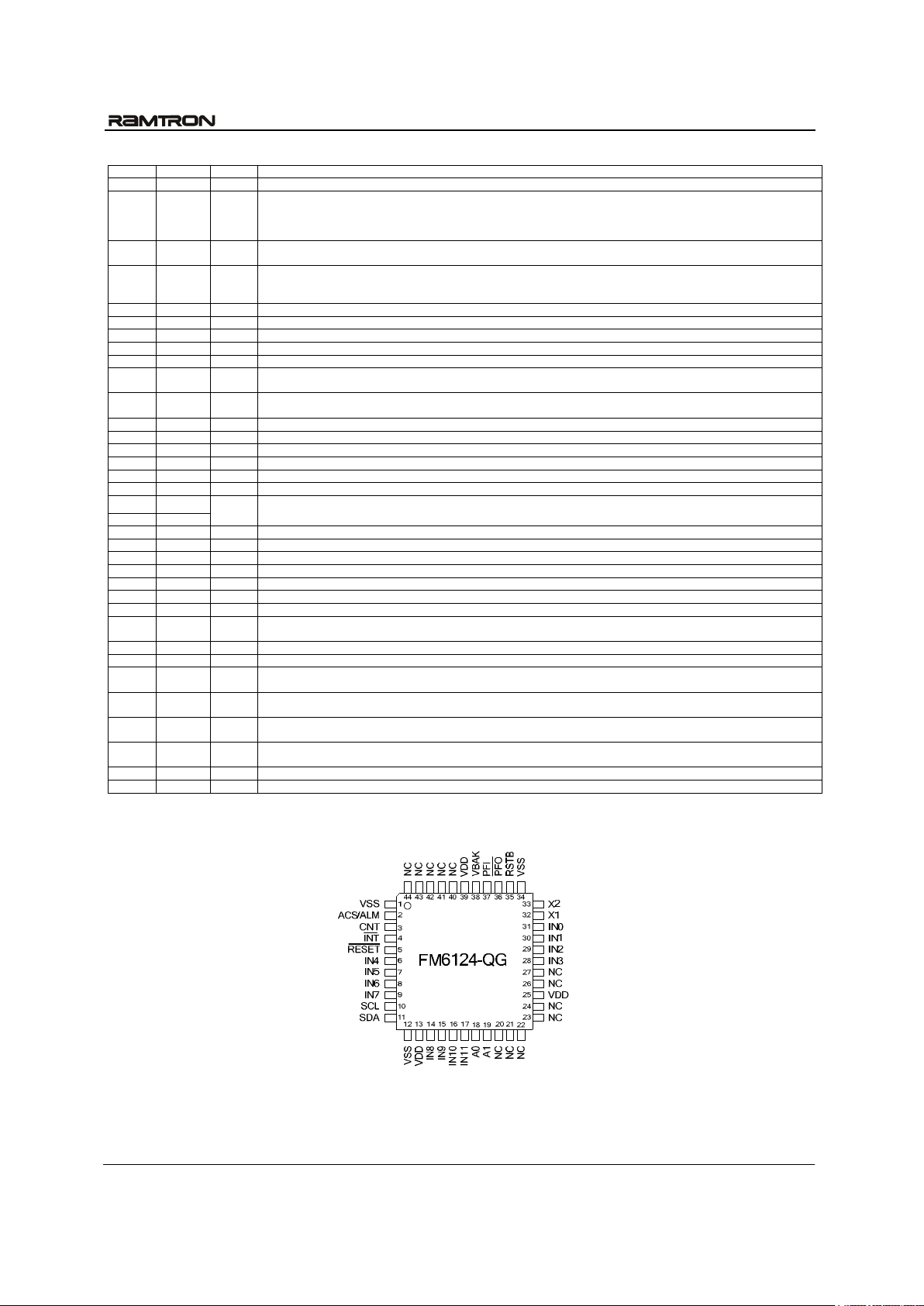
PIN DESCRIPTION
Pin Name I/O Function
1 VSS VSS Ground
2 ACS O
Alarm/Calibration/SquareWave: This is an open-drain output that requires an external pull-up resistor. In normal operation, this
pin acts as the active-low alarm output. In Calibration mode, a 512 Hz square-wave is driven out. In SquareWave mode, the user
may select a frequency of 1, 512, 4096, or 32768 Hz to be used as a continuous output. The SquareWave mode is e ntered by
clearing the AL/SW and CAL bits in register 18h.
3 CNT I
Event Counter Input: This input increments the counter when an edge is detected on this pin. The polarity is programmable and
the counter value is nonvolatile or battery-backed, depending on the mode. This pin should be tied to ground if unused.
4 INT O
Active Low output that can be configured to generate a low level when:
-Event buffer is full
-Activity on event input
5 RESET I Device Reset Input. This active-low input clears all volatile registers. Leave unconnected if not used, pin has internal pull-up.
6 IN4 Event Input Pin 4
7 IN5 Event Input Pin 5
8 IN6 Event Input Pin 6
9 IN7 Event Input Pin 7
10 SCL
Serial Clock: The serial clock input for the two-wire interface. Data is clocked out o f the device on the SCL falling ed ge, and
clocked in on the SCL rising edge. A pull-up resistor is required.
11 SDA
Serial Data/Address: This is a bi-directional pin used to shift serial data and addresses for the two-wire interface. It employs an
open-drain output and is intended to be wire-OR’d with other devices on the two-wire bus. A pull-up resistor is required.
12 VSS VSS Ground
13 VDD Supply Supply voltage
14 IN8 I Event Input Pin 8
15 IN9 I Event Input Pin 9
16 IN10 I Event Input Pin 10
17 IN11 I Event Input Pin 11
18 A0
19 A1
I
Address 1-0: These pins are used to select one of up to 4 devices of the same type on the same two-wire bus. To select the
device, the address value on the three pins must match the corresponding bits contained in the device address.
20-24 NC NC Leave these pins unconnected
25 VDD Supply Supply voltage
26, 27 NC NC Leave these pins unconnected
28 IN3 I Event Input Pin 3
29 IN2 I Event Input Pin 2
30 IN1 I Event Input Pin 1
31 IN0 I Event Input Pin 0
32 X1
32.768 kHz crystal connection. When us ing an externa l oscillator, apply the c lock to X1 a nd a DC mid-leve l to X2 (see Cr ystal
Type section for suggestions).
33 X2 32.768 kHz crystal connection
34 VSS Ground
35 RSTB NC
Reset Out: This active-low output is open dra in with weak pull-up. It is also an input w hen used as a manual reset. This pin
should be left floating if unused.
36 PFO
Early Power-fail Output : This pin is the e arly power-fail outp ut and is typica lly used to drive a microcontroller NMI p in. PFO
drives low when the PFI voltage is <1.5V.
37 PFI
Early Power-fail Input: Typically connected to an unregulated po wer supply to detect an early power failure. This p in must be
tied to ground if unused.
38 VBAK
Backup supply voltage: A 3V battery or a large value capac itor. I f no backup s upply is used, this p in should be tied to V SS a nd
the VBC bit should be cleared.
39 VDD Supply Supply voltage
40-44 NC NC Leave these pins unconnected
QFP-44 PACKAGE PINOUT
Page 3
FM6124 Event Data Recorder
Rev. 1.0
April 2008 Page 3 of 53
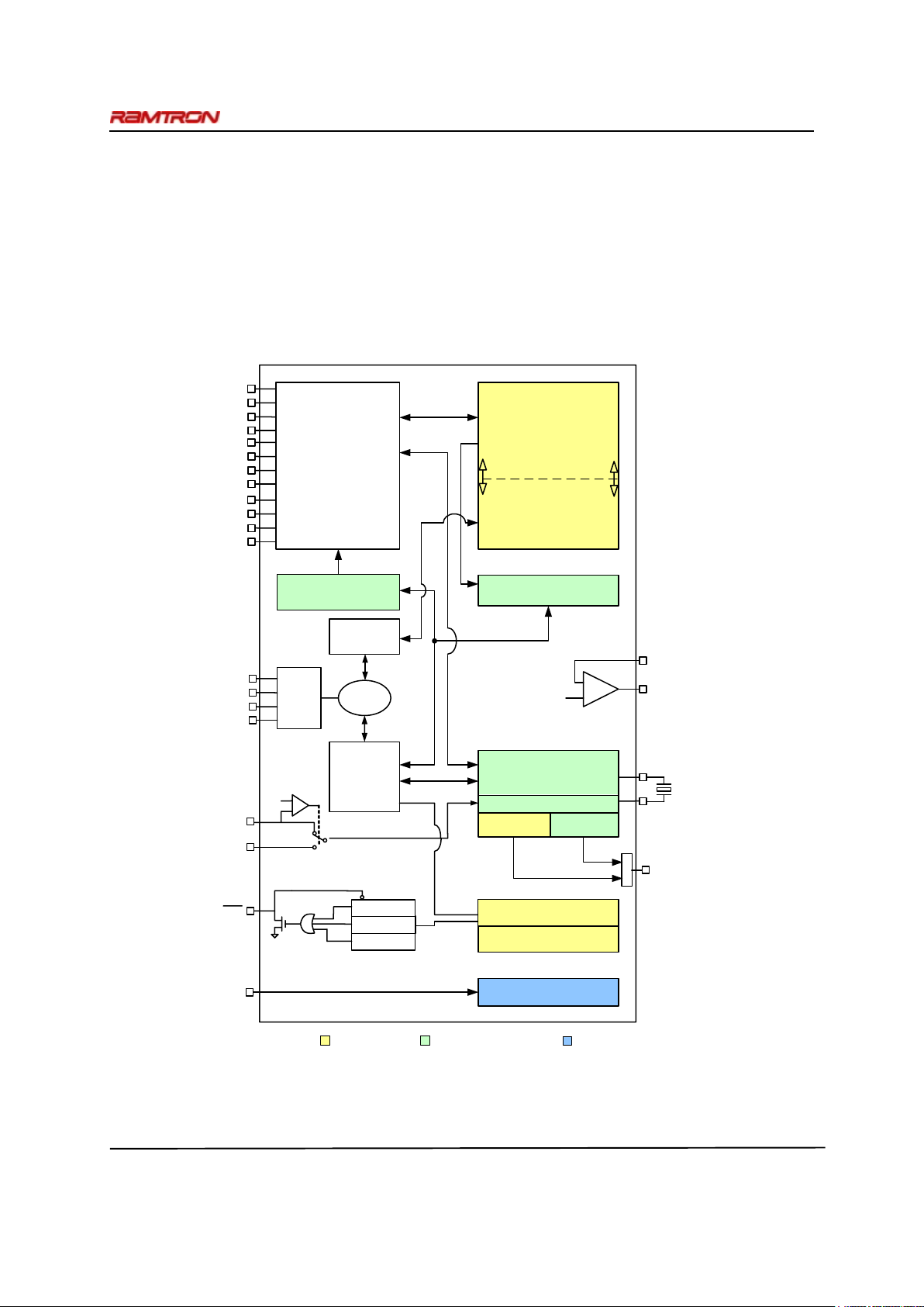
FUNCTIONAL BLOCKS
The functional block diagram of the FM6124 is represented in the figure below. The FM6124 combines the
following:
• 12 input pins individually configurable for Event recording
• Event Buffer memory for event storage implemented as F-RAM
• User accessible F-RAM memory
• User Accessible Real time clock (RTC) with alarm
• MCU co mpanion features such as Eve nt counter, Watchdog T imer, Power Fails Input/Outp ut and
programmable serial number
• I
2
C communication interface supporting two device IDs: one for User-F-RAM (0xA0) and one for
Event Recorder/MCU Companion (0xD0)
I2C
Interface
SDA
A1
RSTB
SCL
VDD
RTC
-
+
RTC Registers
X1
X2
Watchdog
LV Detect
Switched
Power
512Hz/SqW
Battery Backed
Nonvolatile
A0
Battery Backed Event Counter
Alarm
V
SW
NV/BB User Programmable
ManualReset
VBAK
IN4
IN5
IN6
IN7
IN0
IN1
IN2
IN3
IN8
IN9
IN10
IN11
Events Detection and Time
Stamping Unit
Event Recorder Comfiguration
Registers
User Data
F-RAM Zone
F-RAM based
Events Recording
Buffer
0KB
32KB
Adjustable boundary 0KB – 24KB
Event Retrieval Registers
F-RAM Access
Event Recorder
Functions
+
RTC & MCU
companion
Features
I2C ID
Sorting Unit
Serial Number
MCU Companion Features
Registers
AlarmRTC Calibration
CNT
+
-
PFO
PFI
1.5V
External,
User
supplied
32.768KHz
Crystal
ACS
F
IGURE 1.
FM6124 B
LOCK DIAGRAM
Page 4
FM6124 Event Data Recorder
Rev. 1.1
Dec. 2007 Page 4 of 28
Two-wire (I2C) Interface
The FM6124 employs an industry standard two-wire
(I
2
C) bus that is familiar to man y users. This p roduct
is unique since it incorporates two logical devices in
one chip. Each logical device can be accessed
individually and appear to the system software to be
two separate products. One is the nonvolatile FRAM memory device. It has a Slave Address (Slave
ID = 1010b) that operates the same as a stand-alone
memory device. The second device is Event Data
Recorder and Companion which has a different
Slave Address (Slave ID = 1101b).
By convention, any device that is sending data onto
the bus is the transmitter while the tar get device for
this data is the receiver. The device that is
controlling the bus is the master. The master is
responsible for generating the clock signal for all
operations. Any device on the bus that is being
controlled is a slave. The FM6124 is always a slave
device.
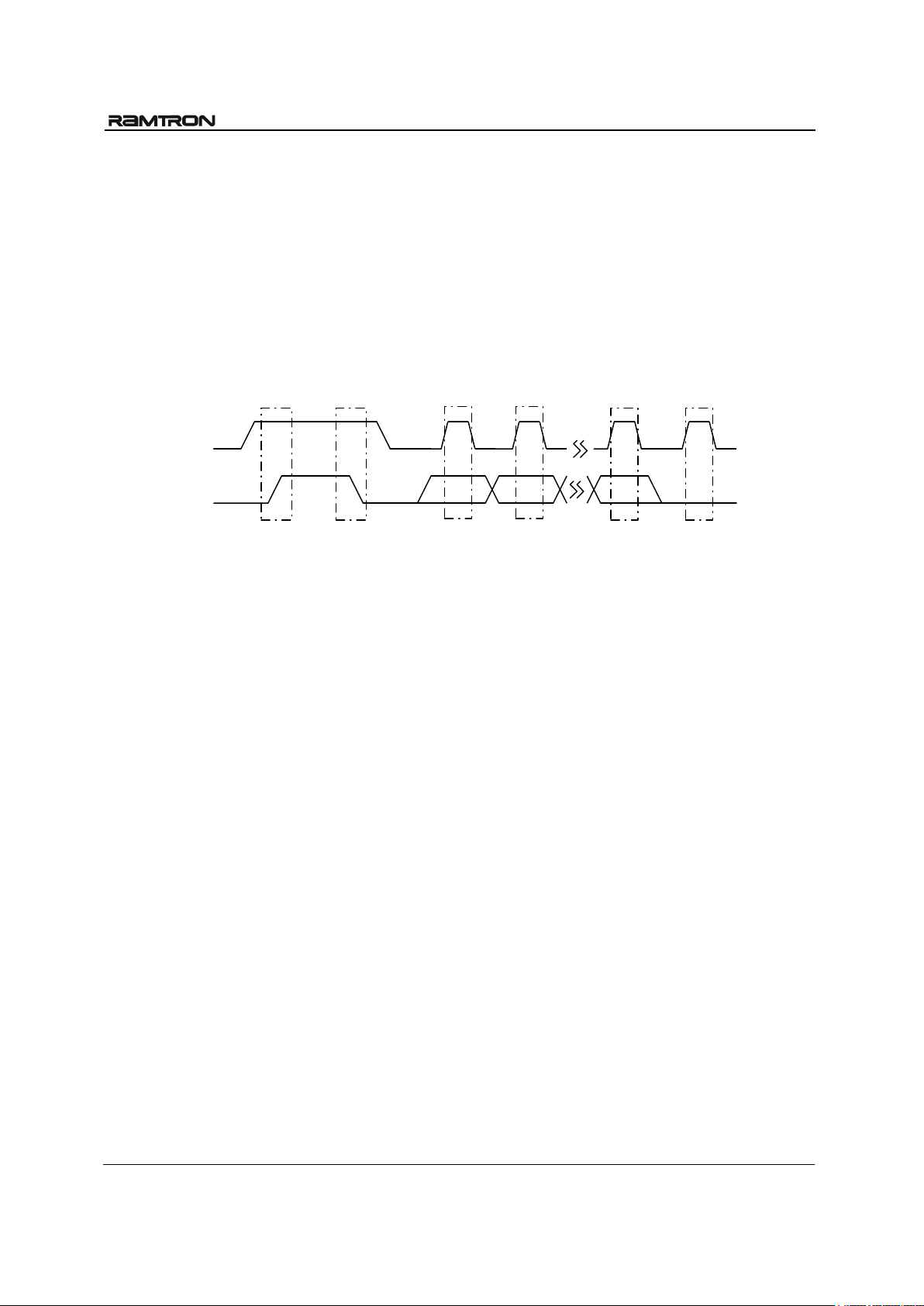
The bus protocol is controlled by transition states in
the SDA and SCL signals. There are four co nditions:
Start, Stop, Data bit, and Acknowledge. The figure
below illustrates the signal conditions that specify
the four states.
Stop
(Master)
Start
(Master)
7
Data bits
(Transmitter)
6
0
Data bit
(Transmitter)
Acknowledge
(Receiver)
SCL
SDA
F
IGURE 2.
I2C B
US CONDITIONS AND TERMINOLOGY
Start Condition
A Start condition is indicated when the bus master
drives SDA from high to lo w while the SCL signal is
high. All read and write transactions begin with a
Start condition. An operation in progress can be
aborted by asserting a Start condition at any time.
Aborting an operatio n using the Start condition will
ready the FM6124 for a new operation.
If the power supply drops below the specified VTP
during operation, any 2-wire transaction in progress
will be aborted and the system must issue a Start
condition prior to performing another operation.
Stop Condition
A Stop condition is indicated when the bus master
drives SDA from low to high while the SC L signal is
high. All operations must end with a Stop condition.
If an operation is pending when a stop is asserted,
the operation will be aborted . The master must have
control of SDA (not a memory read) in order to
assert a Stop condition.
Data/Address Transfer
All data transfers (including addresses) take place
while the SCL signal is high. Except unde r the two
conditions described above, the SDA signal should
not change while SCL is high.
Acknowledge
The Acknowledge (ACK) takes place after the 8
th
data bit has been transferred in any transaction.
During this state the transmitter must release the
SDA bus to allow the receiver to drive it. The
receiver drives the SDA signal low to acknowledge
receipt of the byte. If the receiver does not drive
SDA low, the condition is a No-Acknowledge
(NACK) and the operation is aborted.
The receiver might NACK for two distinct reasons.
First is that a byte transfer fails. In this case, the
NACK ends the current operation so that the part can
be addressed again. This allows the last byte to be
recovered in the event of a communication error.
Second and most common, the receiver does not
send an ACK to deliberately terminate an operation.
For example, during a read operation, the FM6124
will continue to place data onto the bus as long as the
receiver sends ACKs (and clocks). When a read
operation is complete and no more data is needed,
the receiver must NACK the last byte. If the receiver
ACKs the last byte, this will cause the FM6124 to
attempt to drive the bus o n the next clock while the
master is sending a new command such as a Stop.
Page 5

FM6124 Event Data Recorder
Rev. 1.0
April 2008 Page 5 of 53
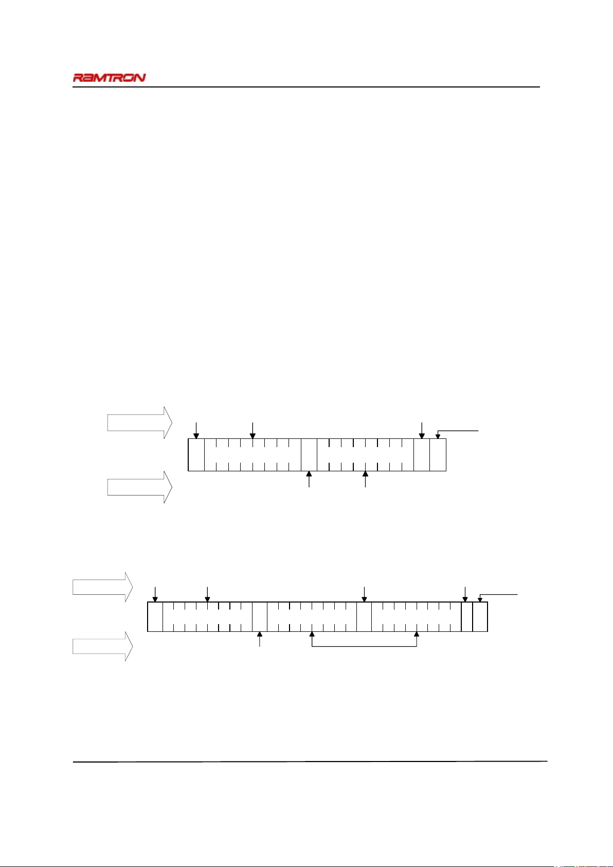
Slave Address
The first byte that the FM6124 expects after a Start
condition is the slave address. As shown in figures
below, the slave address contains the Slave ID,
Device Select address, and a bit that specifies if the
transaction is a read or a write.
The FM6124 has two Slave Addresses (Slave IDs)
associated with two logical devices. To access the
memory device, bits 7-4 should be set to 1010b. The
other logical device within the FM6124 is the Event
Recorder configuration and data access, the real-time
clock and MCU companion. To access this device,
bits 7-4 of the slave address should be set to 1101b.
A bus transaction with this slave address will not
affect the memory in any way. The figures below
illustrate the two Slave Addresses.
The Device Select bits allow multiple device s of the
same type to reside on the 2-wire bus. The device
select bits (bits 2-1) select one of four parts on a twowire bus. They must match the corresponding value
on the external address pins in order to select the
device. Bit 0 is the read/write bit. A “1” indicates a
read operation, and a “0” indicates a write operatio n.
1010XA1A0R/W
Slave ID
Device
Select
76543 21 0
F
IGURE 3. SLAVE ADDRESS - MEMORY
F
IGURE 4. SLAVE ADDRESS –
EDR/C
OMPANION
Addressing Overview – Memory
After the FM6124 acknowledges the Slave Address,
the master can place the memory address on the bus
for a write operation. The address requires two bytes.
The first is the MSB (upper byte). Following the
MSB is the LSB (lower byte) which contains the
remaining eight address b its. The address is latched
internally. Each access causes the latched address to
be incremented automatically. The current address is
the value that is held in the latch, either a newly
written value or the address following the last access.
The current address will be held as long as VDD >
VTP or until a new value is written. Accesses to the
clock do not affect the current memory address.
Reads always use the current address. A random read
address can be loaded by beginning a write operation
as explained below.
After transmission of each data byte, just prior to the
Acknowledge, the FM6124 increments the internal
address. This allows the next sequential byte to be
accessed with no additional addressing externally.
After the last address is reached, the address latch
will roll over to 0000h. There is no limit to the
number of bytes that can be accessed with a single
read or write operation.
Addressing Overview – EDR, RTC & Companion
The Event Recorder, RTC, and Processor
Companion operate in a similar manner to the
memory, except that it uses only one byte of address.
Addresses 00h to 33h corresponds to special function
registers. Attempting to load addresses above 33h is
an illegal condition; the FM6124 will return a
NACK and abort the 2-wire transaction.
Data Transfer
After the address information has been transmitted,
data transfer between the bus master and the
FM6124 begins. For a read, the FM6124 will place 8
data bits on the bus then wait for an ACK from the
master. If the ACK occurs, the FM6124 will transfer
the next byte. If the ACK is not sent, the FM6124
will end the read operation. For a write operation, the
FM6124 will accept 8 data bits from the master then
send an Acknowledge. All data transfer occurs MSB
(most significant bit) first.
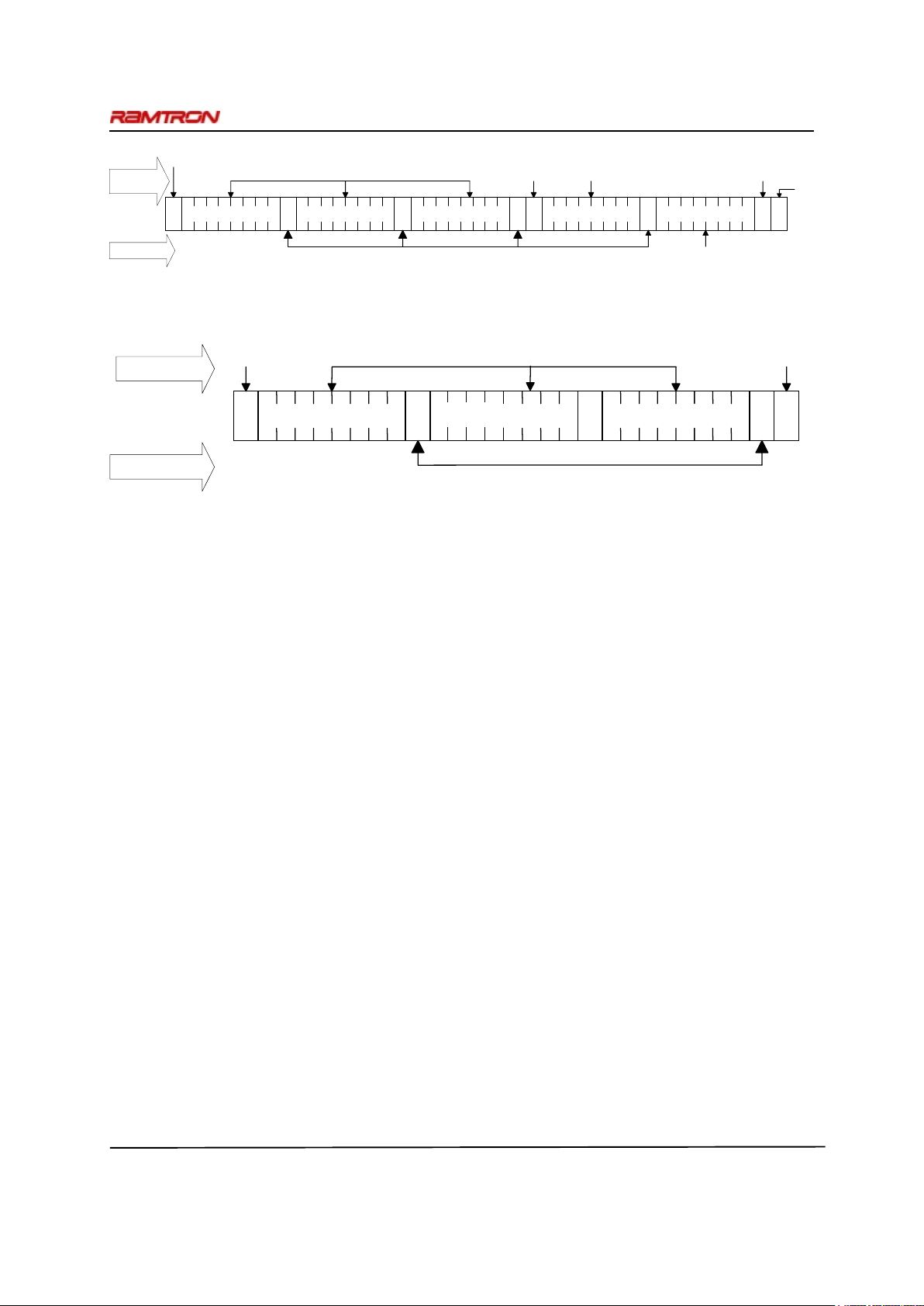
Memory Write Operation
All memory writes begin with a Slave Address, then
a memory address. The bus master indicates a write
operation by setting the slave address LSB to a 0.
After addressing, the bus master sends each byte of
data to the memory and the memory generates an
Acknowledge condition. Any number of sequential
bytes may be written. If t he end of the add ress range
is reached internally, the address counter will wrap
to 0000h. Internally, the actual memory write occurs
after the 8
th
data bit is transferred. It will be complete
before the Acknowledge is sent. Therefore, if the
user desires to abort a write without altering the
memory contents, this sho uld be done using a Start
or Stop condition pr ior to the 8
th
data bit. The figures
that follow illustrate a single - and multiple-writes to
memory.
1
1
0
1
X
A1 A0 R/W
Slave ID
7
6 5
4
3
2
1
0
Device
Select
Page 6
FM6124 Event Data Recorder
Rev. 1.1
Dec. 2007 Page 6 of 28
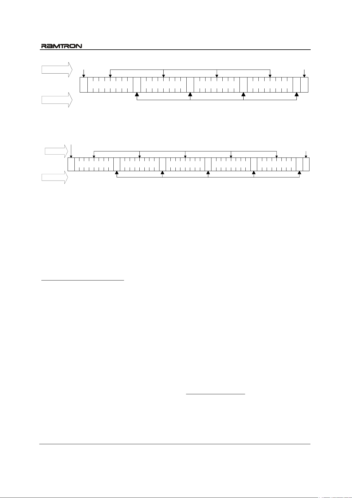
F
IGURE 5. SINGLE BYTE MEMORY WRITE
F
IGURE 6. MULTIPLE BYTE MEMORY WRITE
Memory Read Operation
There are two types of memory read operations. They
are current address read and selective address read. In
a current address read, the FM6124 uses the internal
address latch to supply the address. In a selective
read, the user performs a procedure to first set the
address to a specific value.
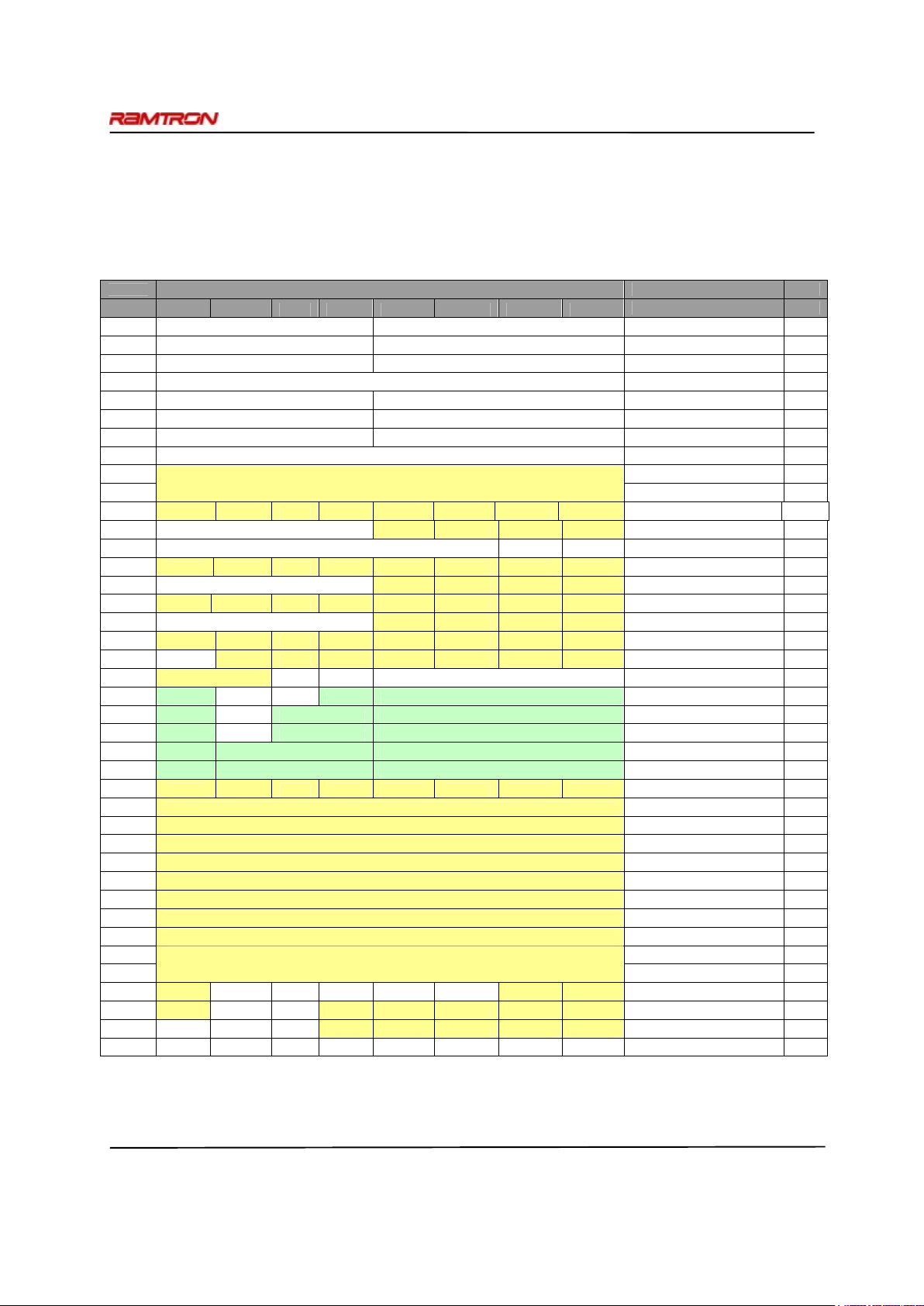
Current Address & Sequential Read
As mentioned above the FM6124 uses an internal
latch to supply the address for a read operation. A
current address read uses the existing value in the
address latch as a starting place for the read
operation. The system reads from the address
immediately following that of the last ope r a tion.
To perform a current address read, the bus master
supplies a slave addr ess with the LSB set to 1. This
indicates that a read operation is requested. After
receiving the complete device address, the FM6124
will begin shifting data out from the current address
on the next clock. The current address is the value
held in the internal address latch.
Beginning with the current address, the bus master
can read any number of bytes. Thus, a sequential read
is simply a current address read with multiple byte
transfers. After each byte the internal address counter
will be incremented.
Each time the bus master acknowledges a byte,
this indicates that the FM6124 should read out
the next sequential byte.
There are four ways to terminate a read operation.
Failing to properly terminate the read will most like l y
create a bus contention as the FM6124 attempts to
read out additional data onto the bus. The four valid
methods follow.
1. The bus master issues a NACK in the 9
th
clock
cycle and a Stop in the 10
th
clock cycle. This is
illustrated in the diagrams below and is
preferred.
2. The bus master issues a NACK in the 9
th
clock
cycle and a Start in the 10
th
.
3. The bus master issues a Stop in the 9
th
clock
cycle.
4. The bus master issues a Start in the 9
th
clock
cycle.
If the internal address reaches the top of me mory, it
will wrap around to 0000h on the next read cycle.
The figures below show the proper operation for
current address reads.
Selective (Random) Read
There is a simple technique that allows a user to
select a random address location as the starting point
for a read operation. This involves using the first
three bytes of a write operation to set the internal
address followed by subsequent read operations.
S
A
Slave Address 0
Address MSB
A
Data Byte
A
P
By Master
By FM6124
Start
A
ddress & Data
Stop
A
cknowledge
A
ddress LSB
A
S
A
Slave Address
0
Address MSB
A
Data Byte
A
P
By Master
By FM6124
Start
Address & Data
Stop
Acknowledge
Address LSB
A
Data Byte
A
Page 7
FM6124 Event Data Recorder
Rev. 1.0
April 2008 Page 7 of 53
To perform a selective read, the bus master sends out
the slave address with the LSB set to 0. This specifies
a write operation. According to the write protocol,
the bus master then sends the address bytes that are
loaded into the internal address latch. After the
FM6124 acknowledges the address, the bus master
issues a Start condition. This simultaneously aborts
the write operation and allows the read command to
be issued with the slave address LSB set to a 1. The
operation is now a read from the current address.
Read operations are illustrated below.
RTC/Companion Write Operation
All RTC and Companio n writes operate in a similar
manner to memory writes. The distinction is that a
different device ID is used and only one byte address
is needed instead of two. Figure 1 0 illustr ates a si ngle
byte write to this device.
RTC/Companion Read Operation
As with writes, a read operation begins with the
Slave Address. To perform a register read, the bus
master supplies a Slave Address with the LSB set to
1. This indicates that a read operation is requested.
After receiving the complete Slave Address, the
FM6124 will begin shifting data out fro m the current
register address on the next clock. Auto-increment
operates for the special function registers as with the
memory address. A current address read for the
registers look exactly like the memory except that the
device ID is different.
The FM6124 contains two separate address registers,
one for the memory address and the other for the
register address. This allows the contents of one
address register to be modifie d without affecting the
current address of the other register. For example,
this would allow an interrupted read to the memory
while still providing fast access to an RTC register. A
subsequent memory re ad will the n continue from the
memory address where it previously left off, without
requiring the load of a new memory address.
However, a write sequence always requires an
address to be supplied.
F
IGURE 7. CURRENT ADDRESS MEMORY READ
F
IGURE 8. SEQUENTIAL MEMORY READ
S
A
Slave Address
1
Data Byte
1 P
By Master
By FM6124
Start
Address
Stop
Acknowledge
No
Acknowledge
Data
S ASlave Address 1 Data Byte 1 P
By Master
By FM6124
Start
A
ddress
Stop
A
cknowledge
No
A
cknowledge
Data
Data Byte
A
A
cknowledge
Page 8
FM6124 Event Data Recorder
Rev. 1.0
April 2008 Page 8 of 53
F
IGURE 9. SELECTIVE (RANDOM) MEMORY READ
F
IGURE
10.
BYTE REGISTER WRITE
Delay When Switching from EDR/Companion ID
to User F-RAM ID
When switching from FM6124 EDR/Companion ID
to the User F-RAM ID, there will be a delay of
~100µs during which the FM6124 may not
acknowledge to I
2
C ID sent to it. This delay is
required for the internal logic of the FM6124 to
perform the switchover from one ID to another.
If the host attempts to initiate a transaction to the
FM6124 with a different slave address within this
100µs period, it is recommended that the host i nitiate
a read command to the FM6124 with the ID projected
to be used with the R/W bit set to 1 and then send a
STOP if the FM6124 fails to respond.
At 100 kHz I
2
C communication speed a 100µS delay
correspond to approximately one I
2
C read command.
This means that if the FM6124 fails to respond to the
first read operation, it will respond on the second one.
S
A
Slave Address
0 A
Data Byte
A P
By Master
Start
Address & Data
Stop
Acknowledge
By FM6124
Register Address
S A
Slave Address
1
Data Byte
1 P
By Master
By FM6124
Start Address
Stop
No
Acknowledge
Data
S
A
Slave Address
0
Address MSB
A
Start
Address
Acknowledge
Address LSB
A
Page 9
FM6124 Event Data Recorder
Rev. 1.0
April 2008 Page 9 of 53
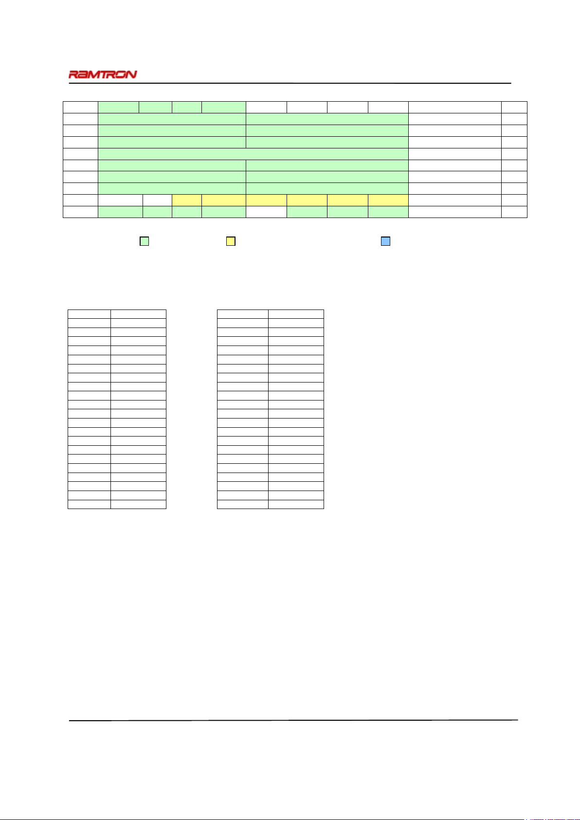
Register Map
The FM6124 Event Recorder, RTC, and processor companion functions are accessed via 51 special function
registers, which are mapped to unique commands. The interface protocol is described in details in the following
pages. The registers contain timekeeping data, alarm settings, control bits, and information flags. A description of
each register follows the summary table.
T
ABLE 1.
FM6124 R
EGISTER MAP OVERVIEW
Address
Data Function Type
7 6 5 4 3 2 1 0
0x33 10 Years Year Event BCD Year RO
0x32 10 Months Month Event BCD Month RO
0x31 10 Date Date Event BCD Dat e RO
0x30 Day of week Event BCD Day of Week RO
0x2F 10 Hours Hours Event BCD Hours RO
0x2E 10 Minutes Minutes Event BCD Minutes RO
0x2D 10 Seconds Seconds Event BCD Seconds RO
0x2C Event Code Event Code RO
0x2B Unread Events Counter MSB RO
0x2A
Number of Unr ead Events Recorded
Unread Events Counter LSB RO
0x29 P11 P10 P9 P8 P7 P6 P5 P4 Pin Pass-through B RO
0x28 Reserved P3 P2 P1 P0 Pin Pass-through A RO
0x27
Reserved
NBEV SNAP
Pin State– #Events snapshot WO
0x26 P11 P10 P9 P8 P7 P6 P5 P4 Pin Event Enable B R/W
0x25 Reserved P3 P2 P1 P0 Pin Event Enable A R/W
0x24 P11 P10 P9 P8 P7 P6 P5 P4 Pin Event Rise/Fall B R/W
0x23 Reserved P3 P2 P1 P0 Pin Event Rise/Fall A R/W
0x22 P11 P10 P9 P8 P7 P6 P5 P4 Pin Event Interrupt B R/W
0x21
CLEAR
BF B75F BHF
P3
P2 P1 P0 Pin Event Interrupt A R/W
0x20 EBUFSIZE[1:0] ERR DIR EDRCMD[3:0] Event Recorder Control R/W
0x1D ~M 0 0 10 mo Month Alarm BCD Month R/W
0x1C ~M 0 10 date Date Alarm BCD Date R/W
0x1B ~M 0 10 hours Hours Alarm BCD Hours R/W
0x1A ~M 10 minutes Minutes Alarm BCD Minutes R/W
0x19 ~M 10 seconds Seconds Alarm BCD Seconds R/W
0x18 SNL
AL/SW
F1 F0 VBC FC VTP1 VTP0 Companion Control R/W
0x17 Serial Number Byte 7 Serial number 7 R/W
0x16 Serial Number Byte 6 Serial number 6 R/W
0x15 Serial Number Byte 5 Serial number 5 R/W
0x14 Serial Number Byte 4 Serial number 4 R/W
0x13 Serial Number Byte 3 Serial number 3 R/W
0x12 Serial Number Byte 2 Serial number 2 R/W
0x11 Serial Number Byte 1 Serial number 1 R/W
0x10 Serial Number Byte 0 Serial number 0 R/W
0x0F Edge Count MSB RO
0x0E
16-bit “CNT Pin” Edge Count
Edge Count LSB RO
0x0D NVC - - - RC WC POLL CP Edge Count Control R/W
0x0C WDE - -
WDET4 WDET3 WDET2 WDET1 WDET0
Watchdog flags R/W
0x0B - - -
WDST4 WDST3 WDST2 WDST1 WDST0
Watchdog flags R/W
0x0A - - - - WR3 WR2 WR1 WR0 Watchdog Restart R/W
Page 10
FM6124 Event Data Recorder
Rev. 1.0
April 2008 Page 10 of 53
0x09 EWDF LWDF POR LB - - - Watchdog flags R/W
0x08 10 year Year BCD Year R/W
0x07 10 month Month BCD Month R/W
0x06 10 date Date BCD Date R/W
0x05 Day of week BCD Day of Week R/W
0x04 10 hours Hours BCD Hours R/W
0x03 10 minutes Minutes BCD Minutes R/W
0x02 10 seconds Seconds BCD Seconds R/W
0x01 CALS CAL4 CAL3 CAL2 CAL1 CAL0 CAL Control R/W
0x00 ~OSCEN AF CF AEN reserved CAL W R RTC Control R/W
Battery-backed = Nonvolatile = BB/NV User Programmable =
Note: When the device is first powered up and programmed, all timekeeping registers must be written because the battery-backed
register values cannot be guaranteed. The table below shows the default values of the nonvolatile registers and some of the
battery-backed bits. All other register values should be treated as unknown
.
Default Register Values
Address Hex Value Address Hex Value
33h 0x00 1Dh 0x81
32h 0x00 1Ch 0x81
31h 0x00 1Bh 0x80
30h 0x00 1Ah 0x80
2Fh 0x00 19h 0x80
2Eh 0x00 18h 0x40
2Dh 0x00 17h 0x00
2Ch 0x00 16h 0x00
2Bh 0x00 15h 0x00
2Ah 0x00 14h 0x00
29h 0x00 13h 0x00
28h 0x00 12h 0x00
27h 0x00 11h 0x00
26h 0x00 10h 0x00
25h 0x00 0Fh 0x00
24h 0x00 0Eh 0x00
23h 0x00 0Dh 0x01
22h 0x00 0Ch 0x00
21h 0x00 0Bh 0x00
20h 0x00 01h 0x00
1Eh-1Fh undefined 00h 0x80
Page 11
FM6124 Event Data Recorder
Rev. 1.0
April 2008 Page 11 of 53
Event Recorder with Timestamp
The main feature of the FM6124 is its event recording
capability. The FM6124 can monitor events occurring on
each of its 12 digital input pins. When an event occurs the
Event is recorded into the Event Buffer F-RAM memory
along with current the timestamp. The recorded event data
is retrieved through I
2
C mapped registers.
The FM6124 is a highly integrated part able to operate in
standalone mode and requiring a few external components
to operate.
Dedicated F-RAM for Event Recording
Based on profiles set by the user, Events are recorded in
nonvolatile F-RAM memory. Each event is timestamped
automatically. A programmable amount of nonvolatile
storage is available to record events (25%, 50%, 75% or
100%). Event recording is triggered by pin state changes.
Events will be recorded in a circular buffer unless emptied
by the host.
A host processor can download the Event log at any time
via the I
2
C interface. In addition the various resources such
as the input pins and the RTC can be read directly through
the serial interface.
Event Definition
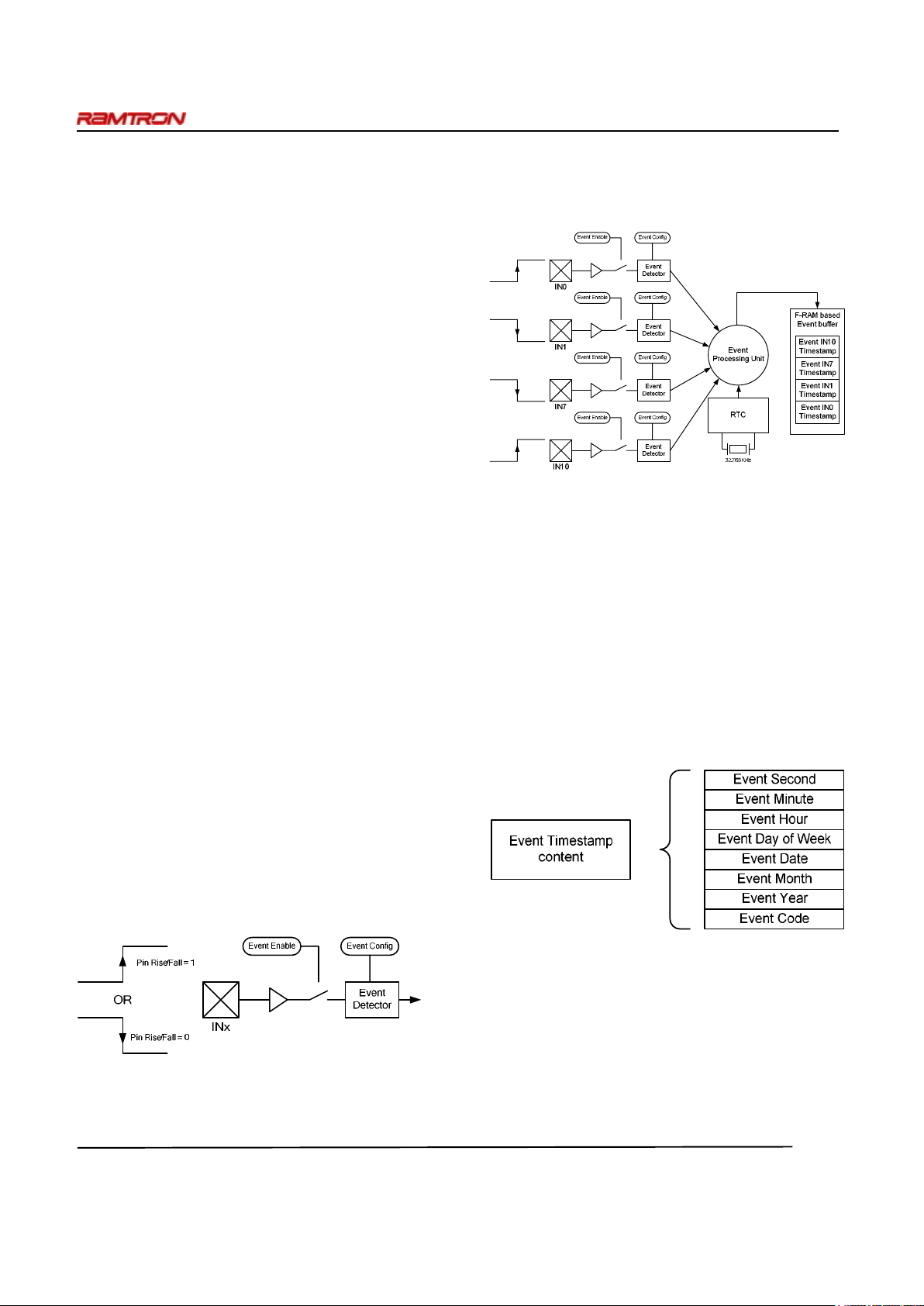
An Event is defined as either a rising or a falling tra nsitio n
occurring on any given input pin. Each one of the input
pin can be individually configured to react on a rising edge
or a falling edge.
Two registers located at addresses 0x23 and 0x24 allow
one to individually configure each one of the FM6124
Input pin to trigger an event record ing on either a Low to
High or a High to Low transitio n
• Setting t he corresponding bit to 1 will trigger an
Event recording on a Low to High transition
• Setting t he corresponding bit to 0 will trigger an
Event recording on a High to Low transition
F
IGURE
11. E
VENT TYPE SUPPORTED
Simultaneous transitions on distinct input pins configured
to react to these transitions will be considered as distinct
events and they will be recorded as such.
F
IGURE
12. E
VENT DETECTION AND STORAGE INTO
F-RAM
The recording order of simultaneous events will be related
to the input numbering. For example, if events occur
simultaneously on IN0, IN1, IN7 and IN10, the first event
recorded will be the one occurring on IN0 followed by the
one on IN1 then IN7 and IN10.
When simultaneous events occur, it is possible that the
timestamp recorded varies by 1 second.
Event Timestamp Content
Each time an event is recorded, the following parameters
are saved in the nonvolatile Event buffer:
F
IGURE
13. E
VENT TIMESTAMP CONTENT
Page 12
FM6124 Event Data Recorder
Rev. 1.0
April 2008 Page 12 of 53
Event Memory/User F-RAM Memory Size
Configuration
The FM6124 contains a total of 32KBytes (256Kb) of FRAM memory on chip. The F-RAM memory can be
configured to serve for both Event Recording and for User
Data saving. The portion of the memory reserved for User
Data is defined through register and occupies the lower
portion of the address range.
The upper portion of the F-RAM addresses is used to store
Event type and timestamp information. The data associated
with Event is accessible only through I
2
C Mapped
registers.
The boundary between User FRAM and Event Recording
FRAM is adjusted through configuration register in the
Event recording portion of the device. The memory
boundary can be changed at any time, however each time it
is changed the entire F-RAM memory (Event Recording/
User Data) will be erased.
The portion of the F-RAM defined as User Memory Data
memory use consistent two-byte addressing for the
memory device rendering it code compatible to the
standalone memory counterparts, such as the FM24xx but
with the ability to be configured up to 24KB in size.
Up to 4000 events can be saved in the FM6124 Event
buffer F-RAM memory. A percentage of the F-RAM can
also be configured as User F-RAM that is accessed like
standard I
2
C based F-RAM and using a dedicated I2C
device ID for User F-RAM access.
The EBUFSIZE[1:0] portion of the Event Data Recorder
control register (address 0x20) defines the portion of
memory reserved for Event recording and User F-RAM
size as shown in the table below:
EBUFSIZE[1:0] Max number of Events User F-RAM size
00 4000 0
01 3000 64 Kb
10 2000 128 Kb
11 1000 192 Kb
When the entire F-RAM memory is reserved for Event
recording, there will be no User F-RAM available and the
FM6124 will stop acknowledging on any I
2
C transactions
initiated with F-RAM / EEPROM device ID.
This allows one to share the I
2
C bus between up to four
FM6124 and up to eight I
2
C based memory devices.
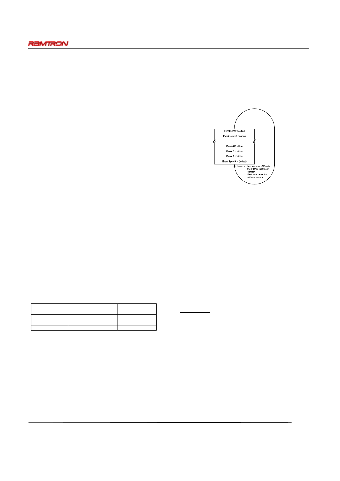
Event Buffer Architecture
The structure of the Event Buffer memory is analogue to a
Circular buffer: Initially the Event data will be stored
from a base address that we will call FP, for First pointer
and up to the maximum number of Event that the FM6124
have been configured to hold. We will call this address
Nmax.
Initially the FP pointer is likel y to be at lowest possible FRAM address. However, when the event buffer is full the
address of the FP pointer will be incremented for each ne w
event recorded.
F
IGURE
14. E
VENT BUFFER OVERVIEW
Event Buffer Pointers
The management of Event recording and retrieval is
handled using nonvolatile F-RAM based virtual pointers.
The addresses where these pointers point to are not directly
accessible through the I
2
C interface however the FM6124
provides commands to control the way those pointers
behave.
Four Pointers are defined:
FP: First pointer
RP: Read Pointer
SP: Stream Pointer
WP: Write pointer
First pointer
The FP pointer is the reference pointer which is fixed for a
given Event recorder configuration.
The first pointer actually indicates the position of oldest
event recorded and it is used as a reference. The
movements of the RP and WP pointers are referenced to
the FP pointer.
Each time the FM6124 configuration is changed through
EBUFSIZE[1:0] register, the p osition o f FP will be reset to
the lowest F-RAM ad dress and it will not move until the
Event buffer is filled.
When the number of event recorded exceeds the buffer
capacity, the FP pointer address will be incremented each
Page 13

FM6124 Event Data Recorder
Rev. 1.0
April 2008 Page 13 of 53
time a new event is recorded in o rder to point to the oldest
event.
Write pointer
The Write pointer is used by the Event recorder to indicate
where the next Event will be recorded in the event buffer.
The WP pointer can only move in one direction: up from
the FP address. For this reason the Eve nt storing can be
seen as a stack: more recent events being stored on top of
older ones.
Eventually the WP pointer can roll over the maximum
address. When this situation occur s the FP pointer will be
incremented for each new event recorded. In applications
where the EDR is placed close to the Host processor it is
possible to configure the Event recorder to activate the
INT output for the follo wi ng situations:
• Buffer Full
• Buffer full at 75%
• Buffer full at 50%
This is done by setting the BF, B75F, B50F bit
respectively in the PINEVENTA register
For situations where the FM6124 is remote from the host
processor, it is always possible for the host processor to
retrieve the number of e vent present in the event buffer b y
reading the Event buffer counter 16-bit register.
Read Pointer
The read pointer RP points to the next event to be read.
This pointer is used to load the next (or previous) event
data into the Event data read back registers (addresses
0x2C to 0x33) whenever the GET command
(EDRCMD[3:0] = 0001 is sent to the FM6124.
Contrary to WP, the Read pointer can be configured to
move from older to newer events but also from newer
event toward older ones.
The direction of the RP pointer depends on:
• The amount of events stored into the Event
memory buffer
• T he value of the READDIR bit
When the READDIR bit is cleared, the RP will fetch e vent
from FP toward WP. However RP cannot move farther
than WP-1. In situation where FP has reached WP-1 any
attempt to read extra events will make the Event data
recorder to fill the Event data read back registers with
0xFF, set the ERR bit of the Event Data recorder
configuration register and the RP address will not be
incremented.
When the READDIR bit is set and the GET co mmand is
initiated, the RP will fetch the data associated with the next
events toward FP and place its content into the Event Data
Read back registers. This provided that the RP pointer is
“away” and up from FP address.
In the case where the GET command is sent to the Event
Recorder while the RP = FP, if there is one event recorded
at FP position its content will be placed in the Event Data
register.
However if from that point a second attempt is made to
read Event Data, the Event Data Recorder will fill the
Event data readback registers with 0xFF, set the ERR bit
of the Event Data recorder configuration register and the
RP address will not be incremented ( decremented).
Stream Pointer
The stream pointer is a dedicated read pointer that is used
for event reading in stream operations. From a functional
point of view the SP pointer is independent of the RP.
However, like the RP po inter, the direction into whic h the
SP pointer will mode, de pend on configur ation of the DIR
bit of the Event Buffer Control register: W hen the DIR bit
is configured as 0, the SP pointer will mode from oldest
event toward newer event. In the situatio n where the DIR
bit is set to 1, the SP pointer moves from newer events
towards older ones.
The value of SP is i nitialized at the moment the ST REAM
command (EDRCMD[3:0] = 0011 is initiated.
The SP pointer is used to automatically load the next event
data into the Event data read back registers (addresses
0x2C to 0x33) after the last register (0x33) of the previous
event content is read and the STREAM Event data
recorder command is maintained.
As other pointers, the SP pointer address is not accessible
to the user.
Page 14
FM6124 Event Data Recorder
Rev. 1.0
April 2008 Page 14 of 53
Retrieving the Number of Unread Events
The FM6124 features a 16-bit register that indicate the
number of unread event present in the Event Buffer
memory. This 16-bit number actually corresponds to the
number of events between WP and RP pointers. It is
accessible through I
2
C registers addresses 0x2A and 0x2B.
Before accessing the Unread Event counter, the host
processor must latch a internal registers content into the
16-bit register.
This is performed by writing 0x02 into the Pin/Event
Snapshot register.
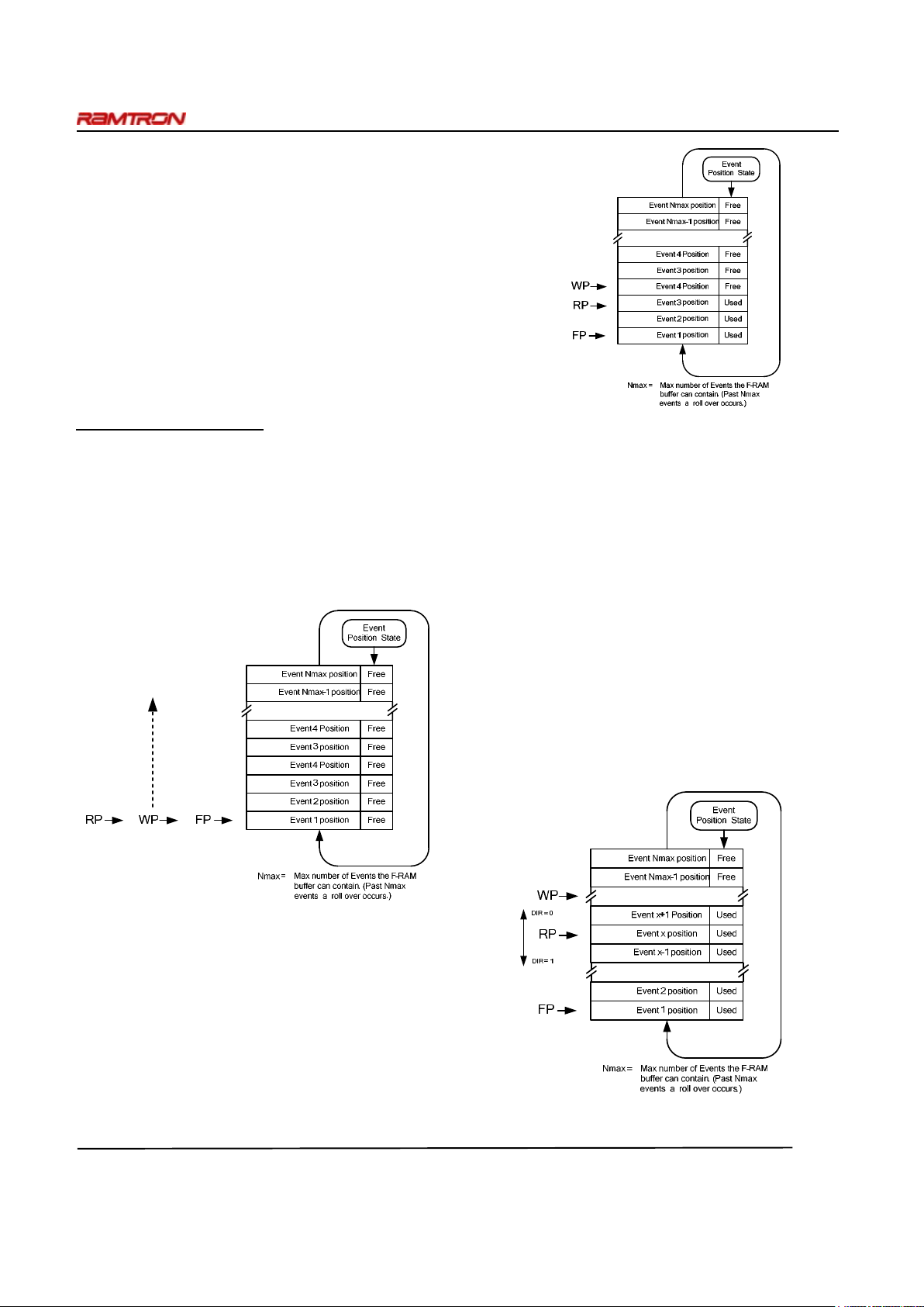
Event buffer initial condition
Every time the FM6124 Event Buffer memory size
configuratio n is c ha nged , b y Eve nt B uffe r M emor y will b e
reinitialized the events records that may still be present
into the F-RAM will be erased. This re-initialization
process takes ~100µs and during that time no eve nts will
be recorded and I
2
C communication should be stopped.
After initialization, the RP, WP, and FP pointer s will all be
pointing at the base memory address as shown in the
diagram below.
WP has only one direction
F
IGURE
15. I
NITIAL CONDITION OF EVENT BUFFER
The following example demonstrates the state of the
pointers after 3 events have been captured and stored in FRAM based Event buffer; the pointers wil l be positioned
as shown in the figure below:
F
IGURE
16. I
NTERNAL POINTERS AFTER 3 EVENTS
The FP, WP, and RP pointers will be set as follow:
• WP will point to the next free position
• RP point to the next Event to be read
• FP is fix
Each time a new Event is recorded the WP address is
incremented. When WP increments beyond the Nmax
position, it will roll-over to FP and so on. If FP reached
WP, an error condition will occur .
As mentioned earlier, after a number of events have been
recorded and a number of events have been read, the RP
pointer will be away from FP and the WP pointer. In that
situation the Event data recor der make s po ssible to retr ieve
either newer or older events by configuring the DIR bit
accordingly. The following diagram illustrates the impact
on the DIR register on the RP operation.
RP direction
depends on DIR bit
F
IGURE
17. RP P
OINTER DIRECTION
Page 15
FM6124 Event Data Recorder
Rev. 1.0
April 2008 Page 15 of 53
EDR COMMAND SET
The FM6124 responds to commands written to address
0x20, through the I
2
C serial port. There are nine unique
commands, eight of which ar e used to retrieve event data,
the remaining one is used to set the partitio n between User
Memory and Event Memory. The commands and their
effect are listed below.
Command EDRCMD[0:3] DIR EFFECT
0 set direction dirrection to increment
1 set p ointer d irrection to decrem ent
0
IF RP ≠ WP THEN
read_bu ffer = event_buffer[RP ]
increment RP
ELSE
read_buffer = [FF,FF,FF,FF,FF,FF,FF,FF]
ERR = 0x01
1
IF RP ≠ FP THEN
read_bu ffer = event_buffer[RP ]
decrement RP
ELSE
read_buffer = [FF,FF,FF,FF,FF,FF,FF,FF]
ERR = 0x01
GET KEEP 0010 x read_buffer = event_buffer[RP]
0
IF RP ≠ WP THEN
read_bu ffer = event_buffer[SP]
increment RP
ELSE
read_buffer = [FF,FF,FF,FF,FF,FF,FF,FF]
ERR = 1
ENDIF
SP = RP
1
IF RP ≠ FP THEN
read_bu ffer = event_buffer[SP]
decrement RP
ELSE
read_buffer = [FF,FF,FF,FF,FF,FF,FF,FF]
ERR = 1
ENDIF
SP = RP
0
IF SP ≠ WP THEN
read_bu ffer = event_buffer[SP]
increment SP
ELSE
read_buffer = [FF,FF,FF,FF,FF,FF,FF,FF]
ERR = 0x01
1
IF SP ≠ FP THEN
read_bu ffer = event_buffer[SP]
decrement SP
ELSE
read_buffer = [FF,FF,FF,FF,FF,FF,FF,FF]
ERR = 0x01
0
IF (WP - RP ) > 1 THEN
increment RP
1
IF RP > FP THEN
decrement RP
FIRS
T
0110 x RP = FP
LAST 0111 x RP = WP - 1
SET EVENT
BUFFER SIZE
1000 x
IF COMMAND[7 :6] ≠ EBUFSIZE[1:0 ] THEN
SP = RP = FP = WP = 0x00
event_buffer = [00,00,00,…,00,00,00]
RESERV ED
1001
to
1111
x No A ction
Table of Comm ands
STREAMING
GET
0011
SET DIR 0000
GET 0001
STREAMING
GET KEEP
0100
SKIP 0101
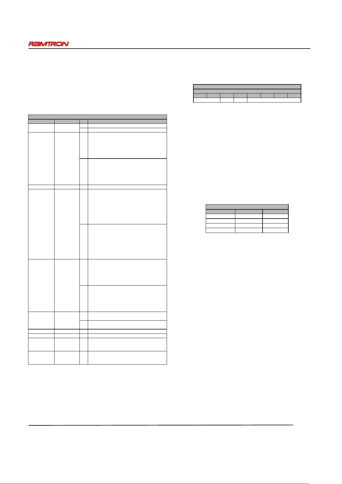
Each command is an eight bit assemblage of lesser
registers EBUFSIZE[1:0], ERR, DIR & EDRCMD[3:0]
The sequence of concatenation is shown in the table
below.
76543210
ERR DIR
Bit
EBUFSI ZE[1 :0] EDRCMD[3:0]
COMMAND STRUCTURE: Address 0x20
The EDRCMD[3:0] register specifies which of the nine
unique commands should be executed.
The DIR register specifies whether the event pointer used
by the command, should be incremented or decremented
after the successful completion of the command.
The ERR register is used to signal the host, that the event
pointer used dur ing the last co mmand ca n move no furt her
in the direction specified by DIR.
The EBUFSIZE[1:0] register specifies the partitioning of
User memory and Event Memory as indicated in the table
below.
EBUFSIZE[1:0] Event Memory User Memory
00 4000 events 0kB
01 3000 events 8kB
10 2000 events 16kB
11 1000 events 24kB
PARTITION SIZE:
ISSUING A COMMAND
When the host is ready to issue a command, the following
procedure should be used.
Start I
2
C
Send the EDR ID & [R/W] = 0 or write
Send the command register start address "0x20"
Send the EBUFSIZE[1:0]& ERR & DIR & EDRCMD[3:0]
Stop I
2
C
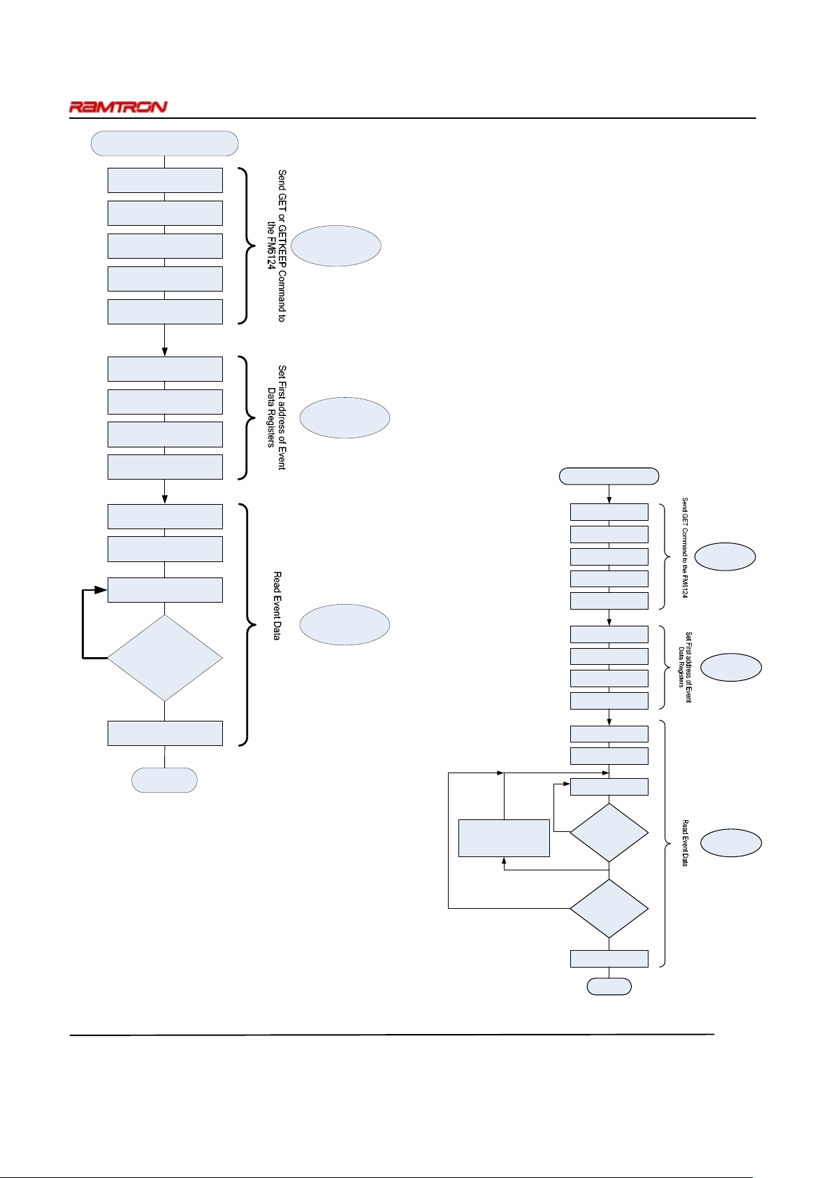
RETRIEVING SINGLE EVENTS
After a GET or KEEP command has been issued, the EDR
will place the event pointed to by RP into the read buffer.
The eight byte wide read buffer can be read through the
I
2
C serial port, starting at address 0x2C and finishing at
address 0x33. To retrieve an event from the buffer, the
following procedure should be followed.
Start I2C
Send the EDR ID & R/W bit = 0 (write)
Send the event buffer start ad dress "0x2C"
Stop I
2
C
Start I
2
C
Send the EDR ID & R/W = 1 (read)
Send seven addition read requests
Stop I
2
C
Page 16
FM6124 Event Data Recorder
Rev. 1.0
April 2008 Page 16 of 53
Single Event Read
Send I2C EDR ID
+ R/W = 0 (write)
I2C Start
Send Reg Address = 0x20
I2C Stop
I2C Start
Send I2C EDR ID
+ R/W = 0 (write)
Send Command: GET or
GETKEEP + set DIR
Send Reg Address = 0x2C
I2C Stop
I2C Start
Send I2C EDR ID
+ R/W = 1 (read)
All 8 Bytes of event
data Read?
Event Data byte Read
I2C Stop
Step 1
Step 2
Step 3
End
F
IGURE
18. S
INGLE EVENT DATA RETRIEVAL PROCESS
Since the EDR's address register is auto-incrementing, it is
unnecessary to send the register address for each byte to be
read from the buffer. It is also unnecessary to begin
reading at address 0x2C or to finish reading at address
0x33. The user is free to retrieve event data from the read
buffer as best suits their application.
If the single event read command issued was a GET, then
RP will be incremented or decremented as indicated by
DIR.
If the single event command issued was a GET KEEP,
then RP will remain unchanged.
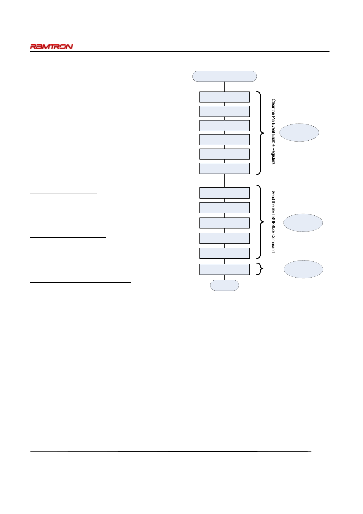
RETRIEVING MULTIPLE EVENTS
After a STREAMING GET or STREAMING GET KEEP
command has been issued, the EDR will place the event
pointed to by the SP pointer, into the read buffer. The
eight byte wide read buffer can be read through the I
2
C
serial port, starting at address 0x2C and finishing at
address 0x33.
To retrieve an event from the buffer, the
following procedure should be followed.
Start I
2
C
Send the EDR ID & [R/W] = 0 or write
Send the event buffer start address "0x2C"
Stop I
2
C
Start I
2
C
Send the EDR ID & [R/W] = 1 or read
Send seven addition read requests
Stop I
2
C
Repeat until the desired nu mber of events has been retrieved.
Multiple Events Read
Send I2C EDR ID
+ R/W = 0 (write)
I2C Start
Send Reg Address = 0x20
I2C Stop
I2C Start
Send I2C EDR ID
+ R/W = 0 (write)
Send Command: STREAM
+ set DIR
Send Reg Address = 0x2C
I2C Stop
I2C Start
Send I2C EDR ID
+ R/W = 1 (read)
Event Data Register
0x33 Read?
Event Data byte Read
I2C Stop
Step 1
Step 2
Step 3
Keep Reading Event?
No
Yes
Reload Event Data Registers
with Next/Previous Event data
(This operation is automatically
performed by the FM6124)
End
F
IGURE
19. M
ULTIPLE EVENTS RETRIEVAL
Page 17
FM6124 Event Data Recorder
Rev. 1.0
April 2008 Page 17 of 53
Since the EDR's I
2
C address registe r is auto-i ncrementing,
it is unnecessary to send the subsequent address for each
byte read from the buffer. It is also unnecessary to begin
reading at address 0x2C. In order for the EDR to
automatically place the next event pointed to by SP into
the read buffer, you must read address 0x33. With this
single exception, the user is free to retrieve event data from
the read buffer as best suits their application.
If the multiple event read command issued was a
STREAMING GET, then RP will be incremented or
decremented as indicated by DIR.
If the multiple event read command issued was a
STREAMING GET KEEP, then RP will remain
unchanged.
Event Skipping Command
The SKIP Command (0101) can be used to increment RP
(DIR = 0) or decrement RP (DIR = 1). Note that RP will
always stay at least one Event before WP and that it will
never be decremented “below” FP.
FIRST and LAST Commands
With the FIRST command, the user can move RP to the
oldest Event immediately (RP = FP)
With the LAST command, the user can move RP to the
newest Event immediately (RP = WP -1)
SET EVENT BUFFER SIZE Command
The SET EVENT BUFFER SIZE command will write the
current value of EBUFSIZE[1:0] to the control register.
The EBUFSIZE[1:0] register is onl y written to the control
register during a SET EVENT BUFFER SIZE command
and ignored at all other times.
When a SET EVENT BUFFER SIZE command is issued
with a new EBUFSIZE[1:0] value, the event data memory
is reinitialized and the event records sto red there are lost.
Reinitialization will only occur if the current value of
EBUFSIZE[1:0] is different than the value stored in the
control register.
Reinitialization takes approximately 100µs to complete
and during this period no event records can be generated
and I
2
C communication should be suspended. Before
issuing a SET EVENT BUFFER SIZE command, it is
recommended to first disable event recording by clearing
the pin event registers A & B, at addresses 0x25 & 0x26
respectively.
The following procedure should be used.
SET BUFSIZE Command
Send I2C EDR ID
+ R/W = 0 (write)
I2C Start
Send Reg Address = 0x25
I2C Stop
I2C Start
Send I2C EDR ID
+ R/W = 0 (write)
Sent 0x00 to Clear Pin
Event Enable A register
Send Reg Address = 0x20
EDR Control Register
I2C Stop
Step 1
Step 2
Sent 0x00 to Clear Pin
Event Enable B register
Sent EBUFSIZE[1:0], 0,
READDIR, EDRCMD[3:0 ]
Wait 100us
End
Step 3
F
IGURE
20. S
ET BUFFER SIZE COMMAND
In situations where the buffer size is unchanged but its
content and pointers needs to be reinitialized, the host
system should perform the following operations:
1. Clear the Pin Event Enable registers (Step 1 of
previous diagram)
2. Send t he SET EVENT BUFFER SI ZE command
with a different EBUFSIZE[1:0] than the current
one (Step 2 of previous diagram)
3. Wait 100µS for the initialization process to
complete (Step 3 of previous diagram)
4. Send t he SET EVENT BUFFER SI ZE command
with the desired EBUFSIZE[1:0] value (Step 2 of
previous diagram, repeat)
5. Wait 100µS for the initialization process to
complete (Step 3 of previous diagram, repeat)
Page 18

FM6124 Event Data Recorder
Rev. 1.0
April 2008 Page 18 of 53
RSTB and RESET input pins
The FM6124 features an active-low RESET input pin.
Applying a manual reset or a power-up Reset of the
FM6124 will clear the volatile registers. However this will
have no impact on the Event buffer content, their
associated pointers, or the MCU companion registers.
The RESET pin features an internal pull-up resistor so if
the reset pin in not used, it can be left unconnected.
Event Deletion
Events are not actually deleted until the circular buffer is
overwritten with new data. Pointers are moved to
effectively prevent access to automatically discarded data.
A pointer move is the last thing done when an event is
popped off of the buffer.
Safety provisions
To prevent data loss or corr uption while Events are being
read with the KEEP bit set to 0, Event Read Pointer is only
moved at the following times:
• After all of the data of an event has been stored
• After the 8
th
data byte is transmitted when
steaming Events
• As soo n as 1 b yte is writte n o ver the o ldest E ven t,
when recording an Event in a full buffer condition
The recording of the event data in the F-RAM Event buffer
memory require ~100µS per event. In the case of
simultaneous events occurring on all 12 input of the
FM6124, a total of 12 x 100µS = 1.2ms will be required
for the recording of all event Data. During that period of
time, event can still be registered, but the Event content
will be held into volatile registers.
If the supply voltage is lost before the completion of all
events data transfer into F-R AM memory, the events that
are still in volatile register will be lost. T he device will
resume normal operation when the supply comes back.
Pin Snapshot
It is possible to see the state of any pin at any time. Write 1
to the SNAP bit to capture the state of all pins. This bit
will be automatically cleared (Write-Only).
Error Conditions
In situations where an error condition ca n occur, data sent
back will be 0xFF. This includ es reading illegal addresses
and requesting more events and the buffer currently holds.
The ERR bit will be set to 1 and Event register s will be set
to 0xFF until Control Buffer i s written.
Output Interrupt: INT pin
The INT pin is an active low output that will react on:
• Any event occurring on any input pin for which
the corresponding bit of the “Gen. INT pulse on
Pin Event” Registers have been set to 1.
• Full Buffer condition.
The setting of the “Gen. INT pulse on Pin Eve nt” registers
and resulting activity on INT pin is independent of
corresponding event recording activation.
MCU Companion
The FM6124 includes a real-time clock (RTC) with alarm
and a processor companion along with the EDR serial
nonvolatile F-RAM. The comp anion is a highly integrated
peripheral including a low-V
DD
reset, a programmable
watchdog timer, a 16-bit nonvolatile event counter, a
comparator for early power-fail detection or other
purposes, and a 64-bit serial number.
The real-time clock and supervisor functions are accessed
under their own commands. The RTC/alarm and some
control registers are maintained by the power source on the
VBAK pin, allowing them to operate from battery or
backup capacitor power when V
DD
drops below a set
threshold.
Processor Supervisor
Supervisors provide a host processor two basic functions:
Detection of power supply fault conditions and a watchdog
timer to escape a software lockup condition. The FM6124
device has a reset pin (RSTB) to drive a processor reset
input during power faults, power-up, and software lockups.
It is an open drain output wit h a weak internal pull-up to
V
DD
. This allows other reset sources to be wire-OR’d to
the RSTB pin. When V
DD
is above the programmed trip
point, RSTB output is pulled weakly to V
DD
. If VDD drops
below the reset trip point voltage level (V
TP
), the RSTB
pin will be drive n low. It will remai n low until V
DD
falls
too low for circuit ope ratio n whic h is the V
RST
level. When
V
DD
rises again above VTP, RSTB continues to dr ive low
for at least 50 ms (t
RPU
) to ensure a robust system reset at a
reliable V
DD
level. After t
RPU
has been met, the RSTB pin
will return to the weak high state. While RSTB is asserted,
serial bus activity is locked out even if a transaction
Page 19
FM6124 Event Data Recorder
Rev. 1.0
April 2008 Page 19 of 53
occurred as VDD dropped below VTP. A memory op eration
started while V
DD
is above VTP will be completed
internally.
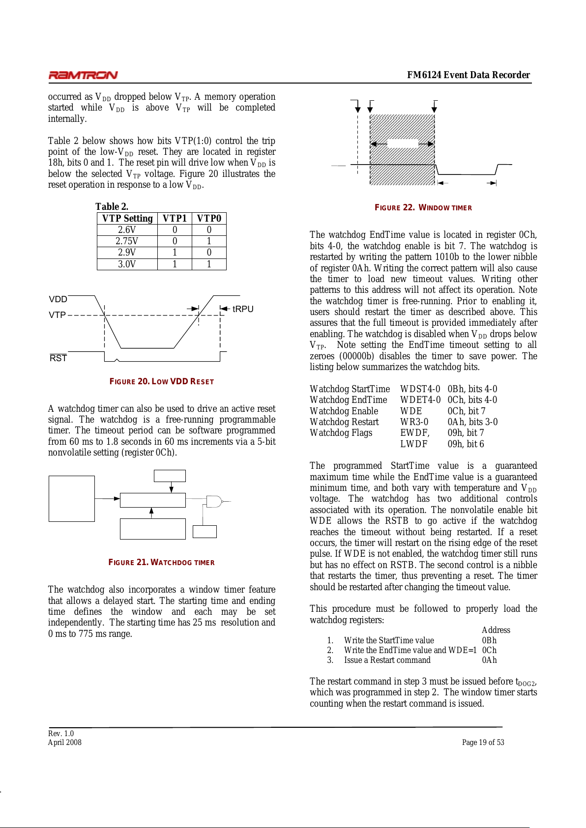
Table 2 below shows how bits VTP(1:0) control the trip
point of the low-V
DD
reset. They are located in register
18h, bits 0 and 1. The reset pin will drive low when V
DD
is
below the selected V
TP
voltage. Figure 20 illustrates the
reset operation in response to a low V
DD
.
Table 2.
VTP Setting VTP1 VTP0
2.6V 0 0
2.75V 0 1
2.9V 1 0
3.0V 1 1
VDD
VTP
tRPU
RST
F
IGURE
20. L
OW
VDD R
ESET
A watchdog timer can also be used to drive an active reset
signal. The watchdog is a free-running programmable
timer. The timeout period can be software programmed
from 60 ms to 1.8 seconds in 60 ms increments via a 5-bit
nonvolatile setting (register 0Ch).
F
IGURE
21. W
ATCHDOG TIMER
The watchdog also incorporates a window timer feature
that allows a delayed start. The starting time and ending
time defines the window and each may be set
independently. The starting time has 25 ms resolution and
0 ms to 775 ms range.
F
IGURE
22. W
INDOW TIMER
The watchdog EndTime value is located in register 0Ch,
bits 4-0, the watchdog enable is bit 7. The watchdog is
restarted by writing the pattern 1010b to the lower nibble
of register 0Ah. Writing the c orrect pattern will also cause
the timer to load new timeout values. Writing other
patterns to this address will not affect its operation. Note
the watchdog timer is free-running. Prior to enabling it,
users should restart the timer as described above. This
assures that the full timeout is provided immediately after
enabling. The watchdog is disabled when V
DD
drops below
V
TP
. Note setting the EndTime timeout setting to all
zeroes (00000b) disables the timer to save power. The
listing below summarizes the watchdog bits.
Watchdog StartTime WDST4-0 0Bh, bits 4-0
Watchdog EndTime WDET4-0 0Ch, bits 4-0
Watchdog Enable WDE 0Ch, bit 7
Watchdog Restart WR3-0 0Ah, bits 3-0
Watchdog Flags EWDF, 09h, bit 7
LWDF 09h, bit 6
The programmed StartTime value is a guaranteed
maximum time while the EndTime value is a guaranteed
minimum ti me, and both vary wit h temperature and V
DD
voltage. The watchdog has two additional controls
associated with its operation. The nonvolatile enable bit
WDE allows the RSTB to go active if the watchdog
reaches the timeout without being restarted. If a reset
occurs, the timer will restart on the risi ng edge of the reset
pulse. If WDE is not enabled, the watchdog timer still r uns
but has no effect on RSTB. The second control is a nibble
that restarts the timer, thus preventing a reset. The timer
should be restarted after changing the timeout value.
This procedure must be followed to properly load the
watchdog register s:
Address
1. Write the StartTime value 0Bh
2. Write the EndTime value and WDE=1 0Ch
3. Issue a Restart command 0Ah
The restart command in step 3 must be issued before t
DOG2
,
which was programmed in step 2. The window timer starts
counting when the restart command is issued.
RST
Watchdog
Restart
Start
Time
End
Time
100 ms (max)
Window
Timebase
Down Counter
Watchdog
Timer Settings
100 ms
clock
WDE
RSTB
WR3-0
= 1010b
to restart
Page 20
FM6124 Event Data Recorder
Rev. 1.0
April 2008 Page 20 of 53
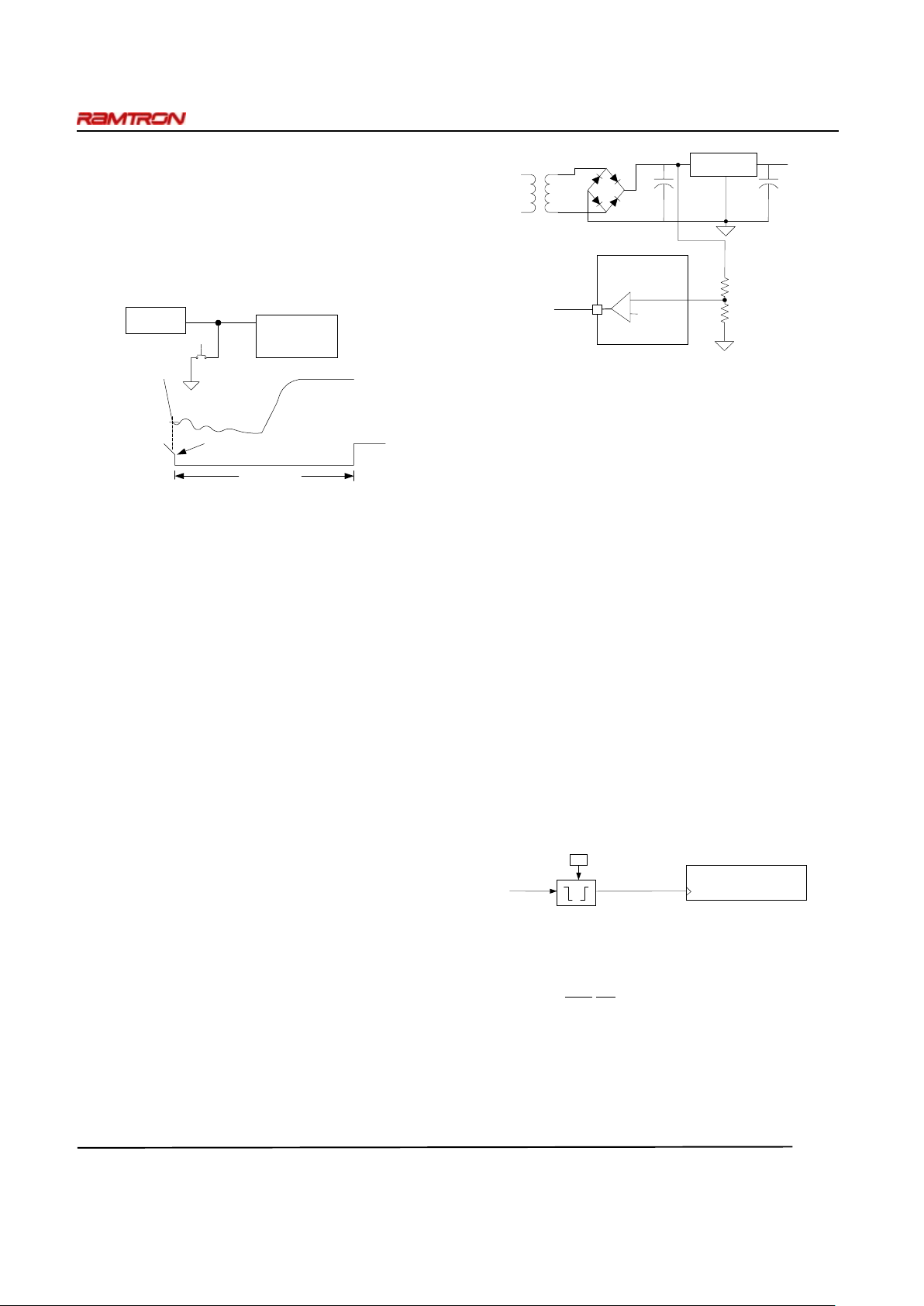
Manual Reset
The RSTB is a bi-directional signal allowing the FM6124
to filter and de-bounce a manual re set switch. The RSTB
input detects an external low condition and responds by
driving the RSTB signal low for 100 ms (max.). This
effectively filters and de-bo unces a reset switch. After this
timeout (t
RPW
), the user may continue pulli ng down on the
RSTB pin, but I
2
C commands will not be locked out.
F
IGURE
23. M
ANUAL RESET
Note the internal weak pull-up eliminates the need for
additional external components.
Reset Flags
In case of a reset condition, a flag bit will be set to ind icate
the source of the reset. A low-V
DD
reset is indicated by the
POR bit, register 09h bit 5. There are two watchdog reset
flags - one for an early fault (EWDF) and the other for a
late fault (LWDF), located in register 09 h bits 7 and 6. A
manual reset will result i n no flag be ing set, so t he abse nce
of a flag is a manual reset. Note that the bits are set in
response to reset sources but they must be cleared by the
user. It is possible to read the register and have both
sources indicated if both have occurred since the user
cleared them.
Power Fail Comparator
An analog comparator compares the PFI input pin to an
onboard 1.5V reference. When the PFI input voltage drops
below this threshold, the comparator will drive the PFO
pin to a low state. The comparator has 100 mV of
hysteresis (rising voltage only) to reduce noise sensitivity.
The most common application of this comparator is to
create an early warning power fail interrupt (NMI). This
can be accomplished by connecting the PFI pin to an
upstream power supply via a resistor divider. An
application circuit is shown below. The comparator is a
general purpose device and its ap plication is not limited to
the NMI function.
F
IGURE
23. C
OMPARATOR AS POWER FAIL WARNING
If the power-fail comparator is not used, the PFI pin should
be tied to either V
DD
or VSS. Note that the PFO output will
drive to V
DD
or VSS as well.
Event Counter
The FM6124 offers the user a nonvolatile 16-bit event
counter. The input pin CNT has a programmable edge
detector. The CNT pin clocks the counter. The counter is
located in registers 0E-0Fh. When the programmed edge
polarity occurs, the counter will increment its co unt value.
The register value is read by setting the RC bit (register
0Dh, bit 3) to 1. This takes a snapshot of the counter byte
allowing a stable value even if a count occurs during the
read. The register value can be written by first setting the
WC bit (register 0Dh, bit 2) to 1. The user then may clear
or preset the counter by writing to registers 0E-0Fh.
Counts are blocked when the WC bit is set, so the user
must clear the bit to allow counts.
The counter polarity control bit is CP, r egister 0Dh bit 0.
When CP is 0, the counter increments on a falling edge of
CNT, and when CP is set to 1, the counter i ncrements o n a
rising edge of CNT. The polarity bit CP is nonvolatile.
F
IGURE
24. E
VENT COUNTER
The counter does
not wrap back to zero when it reaches the
limit of 65,535 (FFFFh). Care must be taken prior to the
rollover, and a subsequent counter reset operation must
occur to continue counting.
There is also a control bit that allows the user to define the
counter as nonvolatile or battery-backed. The counter is
nonvolatile when the NVC bit (register 0Dh, bit 7) is logic
1 and battery-backed when the NVC bit is logic 0 . Setting
+
-
1.5V ref
Regulator
VDD
FM6124
To MCU
NMI input
PFO
FM6124
Reset
Switch
RSTB
MCU
Switch
Behavior
RSTB
FM6124
drives
100 ms (max.)
16-bit Counter
CNT
CP
Page 21
FM6124 Event Data Recorder
Rev. 1.0
April 2008 Page 21 of 53
the counter mode to battery-backed allows counter
operation under V
BAK
(as well as VDD) power. The lowest
operating voltage for battery-backed mode is 2.0V. When
set to “nonvolatile” mode, the counter operates only when
V
DD
is applied and is above the VTP voltage.
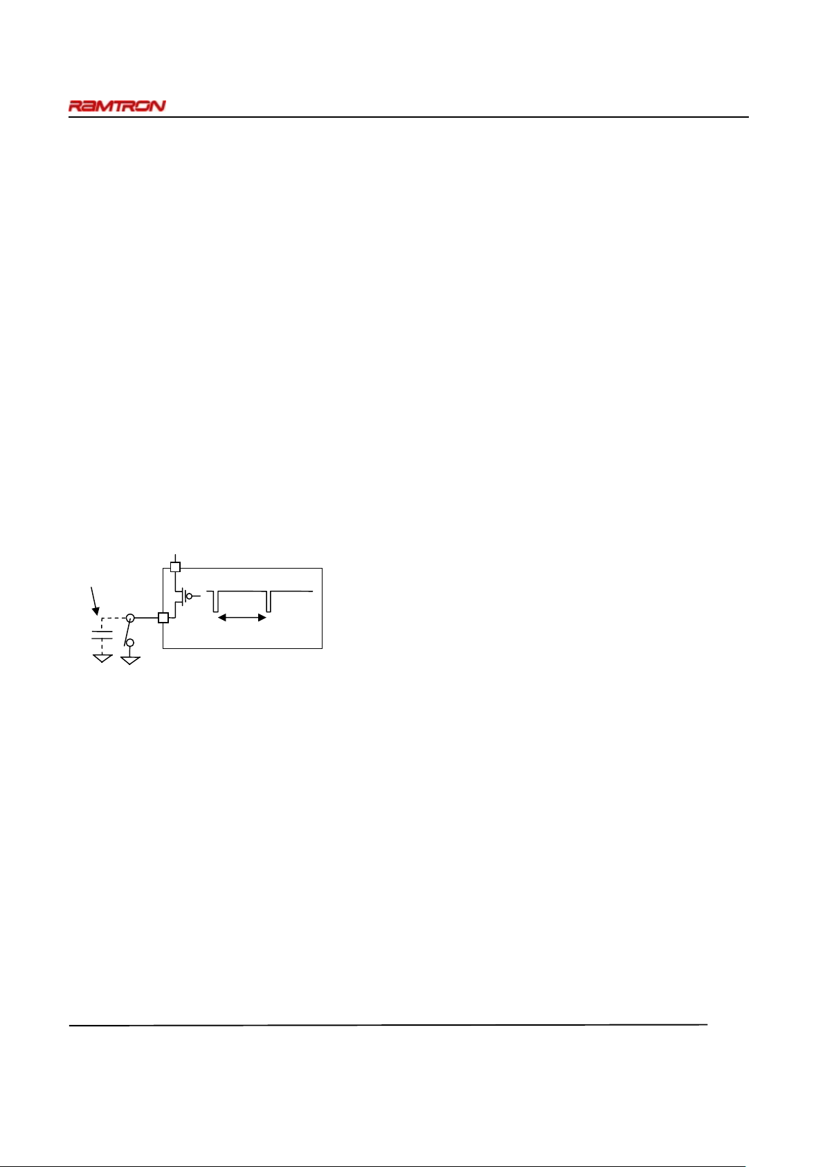
The event counter may be programmed to detect a tamper
event, such as the system’s case or access door being
opened. A normally closed switc h is tied to the CNT pin
and the other contact to the case chassis, usually ground.
The typical solution uses a pull-up resistor on the CNT pin
and will continuously draw battery current. The FM6124
chip allows the user to invoke a polled mode, which
occasionally samples the pin in order to minimize battery
drain. It internally tries to p ull the CNT pin up and if o pen
circuit will be pulled up to a V
IH
level, which will trip the
edge detector and increment the event counter value.
Setting the POLL bit (register 0Dh, bit 1) places the CNT
pin into this mode. This mode allows the event counter to
detect a rising edge tamper event but the user is restricted
to operating in battery-backed mode (NVC=0) and using
rising edge detection (CP=1). The CNT pin is polled once
every 125ms. The additional average I
BAK
current is less
than 5nA. The polling timer circuit operates from the
RTC, so the oscillator must b e enabled for this to function
properly.
F
IGURE
25. P
OLLED MODE ON
CNT
PIN DETECT TAMPER
In the polled mode, the inter nal pullup cir cuit can source a
limited amount of current. The maximum capacitance
(switch open circuit) allowed on the CNT pin is 100pF.
Serial Number
A memory location to write a 64-bit serial number is
provided. It is a writeable nonvolatile memory block that
can be locked by the user once the serial number is set.
The 8 bytes of data and the lock bit are all accessed via
unique commands for the RTC and Processor Companion
registers. Therefore the serial number area is separate and
distinct from the memory array. The serial number
registers can be written an unlimited number of times, so
these locations are general purpose memory. However
once the lock bit is set, the values cannot be altered and
the lock cannot be removed. Once locked the serial number
registers can still be read by the system.
The serial number is located in registers 10h to 17h. The
lock bit is SNL, register 18h bit 7. Setting the SNL bit to a
1 disables writes to the serial number registers, and the
SNL bit cannot be cleared.
Alarm
The alarm function compares user-programmed values to
the corresponding time/date values and operates under V
DD
or V
BAK
power. When a match occurs, an alarm event
occurs. The alarm drives an internal flag AF (register 00h,
bit 6) and may drive the ACS pin, if desired, by setting the
AL/SW bit (register 18h, bit 6 ) in the Companion Contro l
register. The alarm condition is cleared by writing a ‘0’ to
the AF bit.
There are five alarm match fields. They are Month, Date,
Hours, Minutes, and Seconds. Each of these fields also has
a Match bit that is used to determine if the field is used in
the alarm match logic. Setting the Match bit to ‘0’
indicates that the corresponding field will be used in the
match process.
Depending on the Match bits, the alarm can occur as
specifically as one particular second on one day of the
month, or as frequently as once per second continuously.
The MSB of each Alarm register is a Match bit. Examples
of the Match bit settings are shown in T able 4. Selecting
none of the match bits (all ‘1’s) ind icates that no match is
required. The alarm occurs every second. Setting the
match select bit for seconds to ‘0’ causes the logic to
match the seconds alarm value to the current time of day.
Since a match will occur for o nly one value per minute, the
alarm occurs once per minute. Likewise setting the
seconds and minutes match select bits causes an exact
match of these values. Thus, an alarm will occur once per
hour. Setting sec onds, minutes, and hours ca uses a match
once per day. Lastly, selecting all match-values causes an
exact time and date match. Selecting other bit
combinations will not produce meaningful results,
however the alarm circuit will follow the functions
described.
There are two ways a user can detect an alarm event, by
reading the AF flag or monitoring the ACS pin. The
interrupt pin on the host processor may be used to detect
an alarm event. The AF flag in register 00h (bit 6) will
indicate that a time/date match has occurred. The AF flag
will be set to ‘1’ when a match occurs. The AEN bit must
be set to enable the AF flag on alarm matches. The flag
and ACS pin will re main in this state u ntil the AF bit is
cleared by writing it to a ‘0’. Clearing the AEN bit will
prevent further matches from setting AF but will not
automatically clear the AF flag.
The RTC alarm is integrated into the special function
registers and shares its output pin with the 512Hz
CNT
FM6124
125ms
< 100pF
Vbak
Page 22
FM6124 Event Data Recorder
Rev. 1.0
April 2008 Page 22 of 53
calibration and square wave outputs. When the RTC
calibration mode is invoked by setting the CAL bit
(register 00h, bit 2), the ACS output pin will be driven
with a 512 Hz square wave and the alarm will continue to
operate. Since most users only invoke the calibration mode
during production this should have no impact on the
otherwise normal operation of the alarm.
The ACS output may also be used to drive the system with
a frequency other than 512 Hz. The AL/SW bit (register
18h, bit 6) must be ‘0’. A user-selectable frequency is
provided by F0 and F1 (register 18h, bits 4 and 5). The
other frequencies are 1, 4096, and 32768 Hz. If a
continuous frequency output is enabled with CAL mode,
the alarm function will not be available.
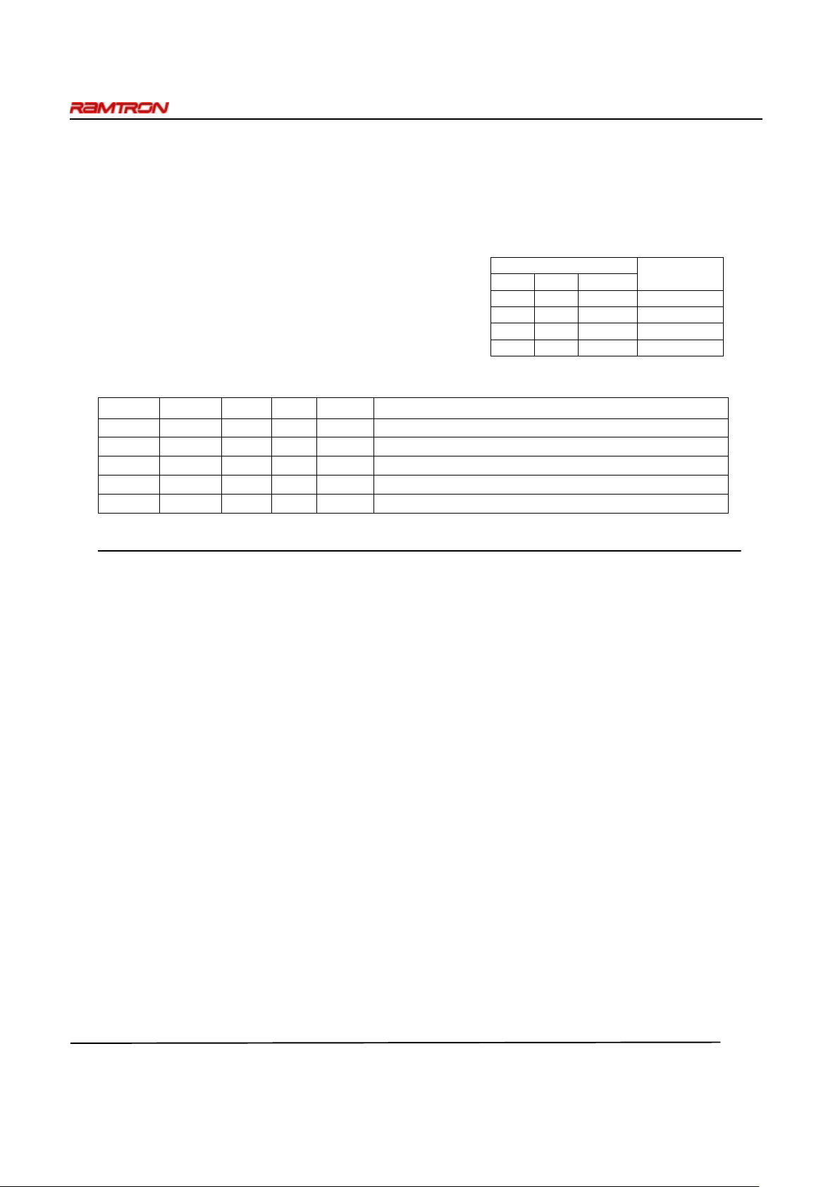
Following is a summary table that shows the relatio nship
between register control settings and the state of the ACS
pin.
Table 3.
State of Register Bit
CAL AEN AL/SW
Function of
ACS pin
0 1 1 /Alarm
0 X 0 Sq Wave out
1 X X 512 Hz out
0 0 1 Hi-Z
Table 4. Alarm Match Bit Examples
Seconds Minutes Hours Date Months Alarm condition
1 1 1 1 1 No match required = alarm 1/second
0 1 1 1 1 Alarm when seconds match = alarm 1/minute
0 0 1 1 1 Alarm when seconds, minutes ma tch = alarm 1/hour
0 0 0 1 1 Alarm when seconds, minutes, hours match = alarm 1/date
0 0 0 0 1 Alarm when seconds, minutes, hours, date match = alarm 1/month
Real-time Clock Operation
The real-time clock (RTC) is a timekeeping device
that can be capacitor- or battery-backed for
permanently-powered operation. It offers a software
calibration feature that allows high accuracy.
The RTC consists of an oscillator, clock divider, and
a register system for user access. It divides down the
32.768 kHz time-base and provides a minimum
resolution of seconds (1 Hz). Static registers provide
the user with read/write access to the time values. It
includes registers for seconds, minutes, hours, dayof-the-week, date, months, and years. A block
diagram shown in Figure 9 illustrates the RTC
function.
The user registers are synchronized with the
timekeeper core using R and W bits in register 00h.
The R bit is used to read the time. Changing t he R bit
from 0 to 1 transfers timekeeping information from
the core into the user registers 02-08h that can be
read by the user. If a timekeeper update is pending
when R is set, then the core will be updated prior to
loading the user registers. The user registers are
frozen and will not be up date d again u ntil the R bit i s
cleared to a ‘0’.
The W bit is used to write new time/date values.
Setting the W bit to a ‘1’ stops the RTC a nd allows
the timekeeping core to be written with new data.
Clearing it to ‘0’ causes the RTC to start running
based on the new values loaded in the timekeeper
core. The RTC may be synchronized to another clock
source. On the 8
th
clock of the write to register 00h
(W=0), the RTC starts counting with a timebase that
has been reset to zero milliseconds.
Note: Users should be certain not to load invalid
values, such as FFh, to the timekeeping registers.
Updates to the timekeeping co re occur continuously
except when locked.
Page 23
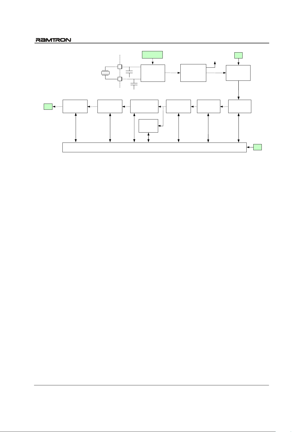
FM6124 Event Data Recorder
Rev. 1.1
Dec. 2007 Page 23 of 28
F
IGURE
26. R
EAL TIME CLOCK CORE BLOCK DIAGRAM
Backup Power
The real-time clock and alarm are intended to be
permanently powered. When the primary system
power fails, the voltage on the VDD pin will drop.
When the VDD voltage is less than V
SW
, the RTC
(and event counter) will switch to the backup power
supply on VBAK. The clock operates at extremely
low current in order to maximize batter y or capacitor
life. However, an advantage of combining a clock
function with F-RAM memor y is that data is not lost
regardless of the backup power source.
Trickle Charger
To facilitate capacitor backup, the VBAK pin can
optionally provide a tric kle charge curre nt. When the
VBC bit (register 18h bit 3) i s set to a ‘1’, the V
BAK
pin will source approximately 80 µA until V
BAK
reaches V
DD
. This charges the capacitor to VDD
without an external diode and resistor charger.
There is a Fast Charge mode which is enabled by the
FC bit (register 18h, bit 2). In this mode the trickle
charger current is set to approximately 1 mA,
allowing a large backup capacitor to charge more
quickly.
• In the case where no battery is used, the V
BAK
pin should be tied to V
SS
and VBC bit cleared.
!
!!
! Note: systems using lithium batteries should clear
the VBC bit to 0 to prevent battery charging. The
VBAK circuitry includes an internal 1 K
Ω
series
resistor as a safety element.
Calibration
When the CAL bit in register 00 h is set to a ‘1’, the
clock enters calibration mode. The FM6124 devices
employ a digital method for calibrating the crystal
oscillator frequency. The digital calibration scheme
applies a digital correction to the RT C counters b ased
on the calibration settings, CALS and CAL.4-0. In
calibration mode (CAL=1), the ACS pin is driven
with a 512 Hz (nominal) square wave and the alarm
is temporarily unavailable. Any measured deviation
from 512 Hz translates into a timekeeping error. The
user measures the frequency and writes the
appropriate correction value to the calibration
register. The correction codes are listed in the table
below. For convenience, the table also shows the
frequency error in ppm. Positive ppm errors require a
negative adjustment that removes pulses. Negative
ppm errors require a positive correction that adds
pulses. Positive ppm adjustments have the CALS
(sign) bit set to 1, where as negati ve p p m adjust ment s
have CALS = 0. After calibratio n, the cloc k will ha ve
a maximum error of ± 2.17 ppm or ± 0.09 minutes
per month at the calibrated temperature.
The user will not be able to see the effect of the
calibration setting on the 512 Hz output. The
addition or subtractio n of digital pulses occurs after
the 512 Hz output.
The calibration setting is stor ed in F -RAM so it is no t
lost should the backup source fail. It is accessed with
bits CAL.4-0 in register 01h. This value only ca n be
written when the CAL bit is set to a 1. To exit the
calibration mode, the user must clear the CAL bit to a
32.768 kHz
crystal
Oscillator
Clock
Divider
Update
Logic
512 Hz or
SW out
W
R
Seconds
7 bits
Minutes
7 bits
Hours
6 bits
Date
6 bits
Months
5 bits
Years
8 bits
CF
Days
3 bits
User Registers
1 Hz
/OSCEN
Page 24
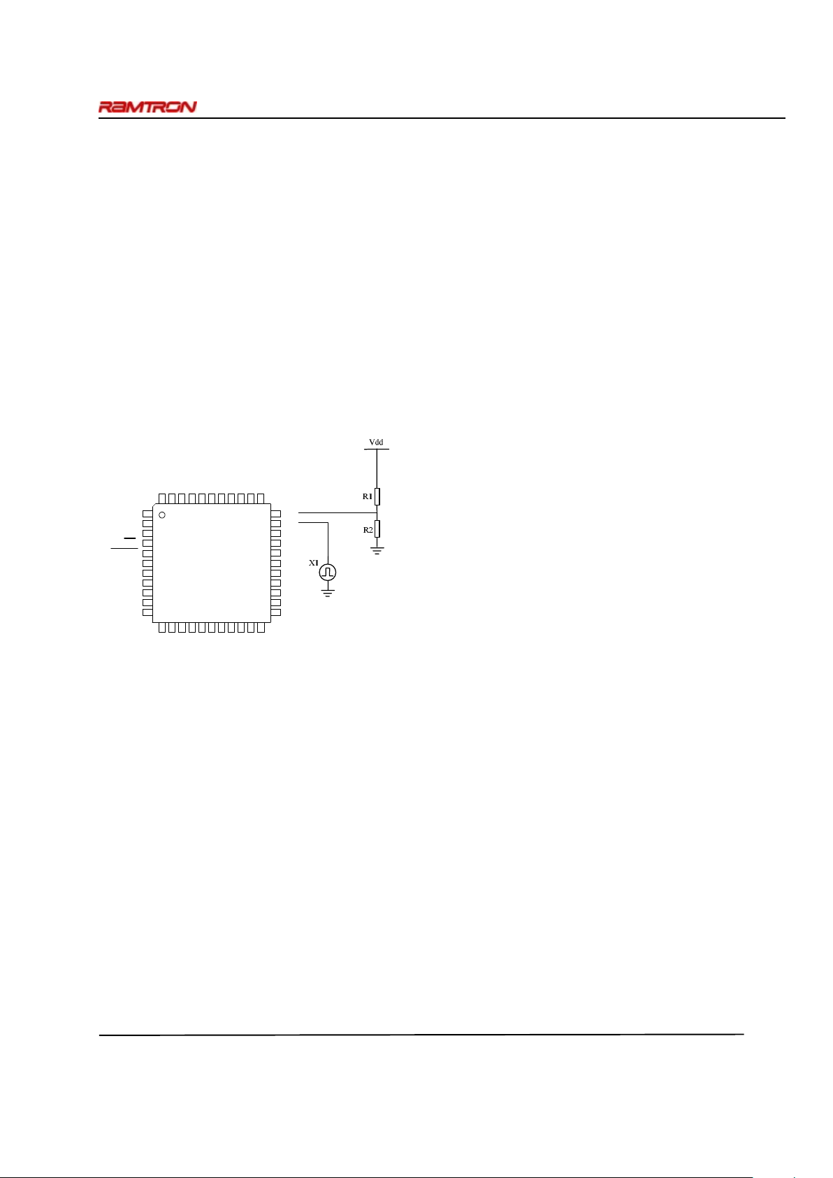
FM6124 Event Data Recorder
Rev. 1.0
April 2008 Page 24 of 53
logic 0. When the CAL bit is 0, the ACS pin will
revert to the function according to Table 3.
Crystal Type
The crystal oscillator is designed to use a 12.5pF
crystal without the need for external components,
such as loading capacitors. The FM6124 device has
built-in loading capacitors that match the crystal.
If a 32.768kHz crystal is not used, an external
oscillator may be connected to the FM6124. Apply
the oscillator to the X1 pin. Its high and lo w voltage
levels can be driven rail -to-rail or amplitudes as low
as approximately 500mV p-p. To ensure proper
operation, a DC bias must be applied to the X2 pin.
It should be centered between the high and low levels
on the X1 pin. This can be accomplished with a
voltage divider .
1
2
3
4
5
6
7
8
9
10
11
3435363738394041424344
FM6124-QG
221 2 13 14 15 16 17 18 19 20 21
23
24
25
26
27
28
29
30
31
32
33
VSS
ACS/ALM
CNT
INT
RESET
IN4
IN5
IN6
IN7
SCL
SDA
VSS
RSTB
PFO
PFI
VBAK
VDDNCNC
NC
NC
NC
X2
X1
IN0
IN1
IN2
IN3
NC
NC
VDD
NC
NC
VSS
VDD
IN8
IN9
IN10
IN11
A0
A1
NCNCNC
F
IGURE
27. E
XTERNAL OSCILLATOR
In the example, R1 and R2 are chosen such that the
X2 voltage is centered around the oscillator drive
levels. If you wish to avoid the DC current, you may
choose to drive X1 with an external clock and X2
with an inverte d clock using a CMOS invert er.
Page 25
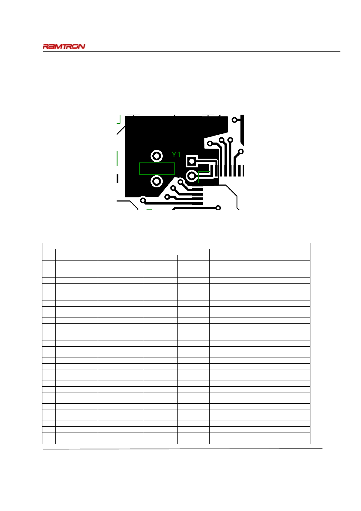
FM6124 Event Data Recorder
Rev. 1.0
April 2008 Page 25 of 53
Layout Recommendations
The X1 and X2 crystal pins employ very high impe dance cir cuits and the oscillato r conne cted to these pins can b e upset by
noise or extra loading. To reduce RTC clock errors from signal switching noise, a guard ring should be placed around these
pads and the guard ring grounded. High speed traces should be routed away from the X1/X2 pads. The X1 and X2 trace
lengths should be less than 5 mm. The use of a ground plane on the backside or inner board layer is preferred. See layout
example below.
F
IGURE
27. PCB L
AYOUT EXAMPLE
Table 5. Digital Calibration Adjustments
Positive Calibration for slow clocks: Calibration will achieve ± 2.17 PPM after calibration
Measured Frequency Range Error Range (PPM)
Min Max Min Max Program Calibration Register to:
0 512.0000 511.9989 0 2.17 000000
1 511.9989 511.9967 2.18 6.51 100001
2 511.9967 511.9944 6.52 10.85 100010
3 511.9944 511.9922 10.86 15.19 100011
4 511.9922 511.9900 15.20 19.53 100100
5 511.9900 511.9878 19.54 23.87 100101
6 511.9878 511.9856 23.88 28.21 100110
7 511.9856 511.9833 28.22 32.55 100111
8 511.9833 511.9811 32.56 36.89 101000
9 511.9811 511.9789 36.90 41.23 101001
10 511.9789 511.9767 41.24 45.57 101010
11 511.9767 511.9744 45.58 49.91 101011
12 511.9744 511.9722 49.92 54.25 101100
13 511.9722 511.9700 54.26 58.59 101101
14 511.9700 511.9678 58.60 62.93 101110
15 511.9678 511.9656 62.94 67.27 101111
16 511.9656 511.9633 67.28 71.61 110000
17 511.9633 511.9611 71.62 75.95 110001
18 511.9611 511.9589 75.96 80.29 110010
19 511.9589 511.9567 80.30 84.63 110011
20 511.9567 511.9544 84.64 88.97 110100
21 511.9544 511.9522 88.98 93.31 110101
22 511.9522 511.9500 93.32 97.65 110110
23 511.9500 511.9478 97.66 101.99 110111
24 511.9478 511.9456 102.00 106.33 111000
25 511.9456 511.9433 106.34 110.67 111001
26 511.9433 511.9411 110.68 115.01 111010
27 511.9411 511.9389 115.02 119.35 111011
28 511.9389 511.9367 119.36 123.69 111100
29 511.9367 511.9344 123.70 128.03 111101
30 511.9344 511.9322 128.04 132.37 111110
31 511.9322 511.9300 132.38 136.71 111111
Page 26

FM6124 Event Data Recorder
Rev. 1.0
April 2008 Page 26 of 53
Negative Calibration for fast clocks: Calibration will achieve ± 2.17 PPM after calibration
Measured Frequency Range Error Range (PPM)
Min Max Min Max Program Calibration Register to:
0 512.0000 512.0011 0 2.17 000000
1 512.0011 512.0033 2.18 6.51 000001
2 512.0033 512.0056 6.52 10.85 000010
3 512.0056 512.0078 10.86 15.19 000011
4 512.0078 512.0100 15.20 19.53 000100
5 512.0100 512.0122 19.54 23.87 000101
6 512.0122 512.0144 23.88 28.21 000110
7 512.0144 512.0167 28.22 32.55 000111
8 512.0167 512.0189 32.56 36.89 001000
9 512.0189 512.0211 36.90 41.23 001001
10 512.0211 512.0233 41.24 45.57 001010
11 512.0233 512.0256 45.58 49.91 001011
12 512.0256 512.0278 49.92 54.25 001100
13 512.0278 512.0300 54.26 58.59 001101
14 512.0300 512.0322 58.60 62.93 001110
15 512.0322 512.0344 62.94 67.27 001111
16 512.0344 512.0367 67.28 71.61 010000
17 512.0367 512.0389 71.62 75.95 010001
18 512.0389 512.0411 75.96 80.29 010010
19 512.0411 512.0433 80.30 84.63 010011
20 512.0433 512.0456 84.64 88.97 010100
21 512.0456 512.0478 88.98 93.31 010101
22 512.0478 512.0500 93.32 97.65 010110
23 512.0500 512.0522 97.66 101.99 010111
24 512.0522 512.0544 102.00 106.33 011000
25 512.0544 512.0567 106.34 110.67 011001
26 512.0567 512.0589 110.68 115.01 011010
27 512.0589 512.0611 115.02 119.35 011011
28 512.0611 512.0633 119.36 123.69 011100
29 512.0633 512.0656 123.70 128.03 011101
30 512.0656 512.0678 128.04 132.37 011110
31 512.0678 512.0700 132.38 136.71 011111
Page 27
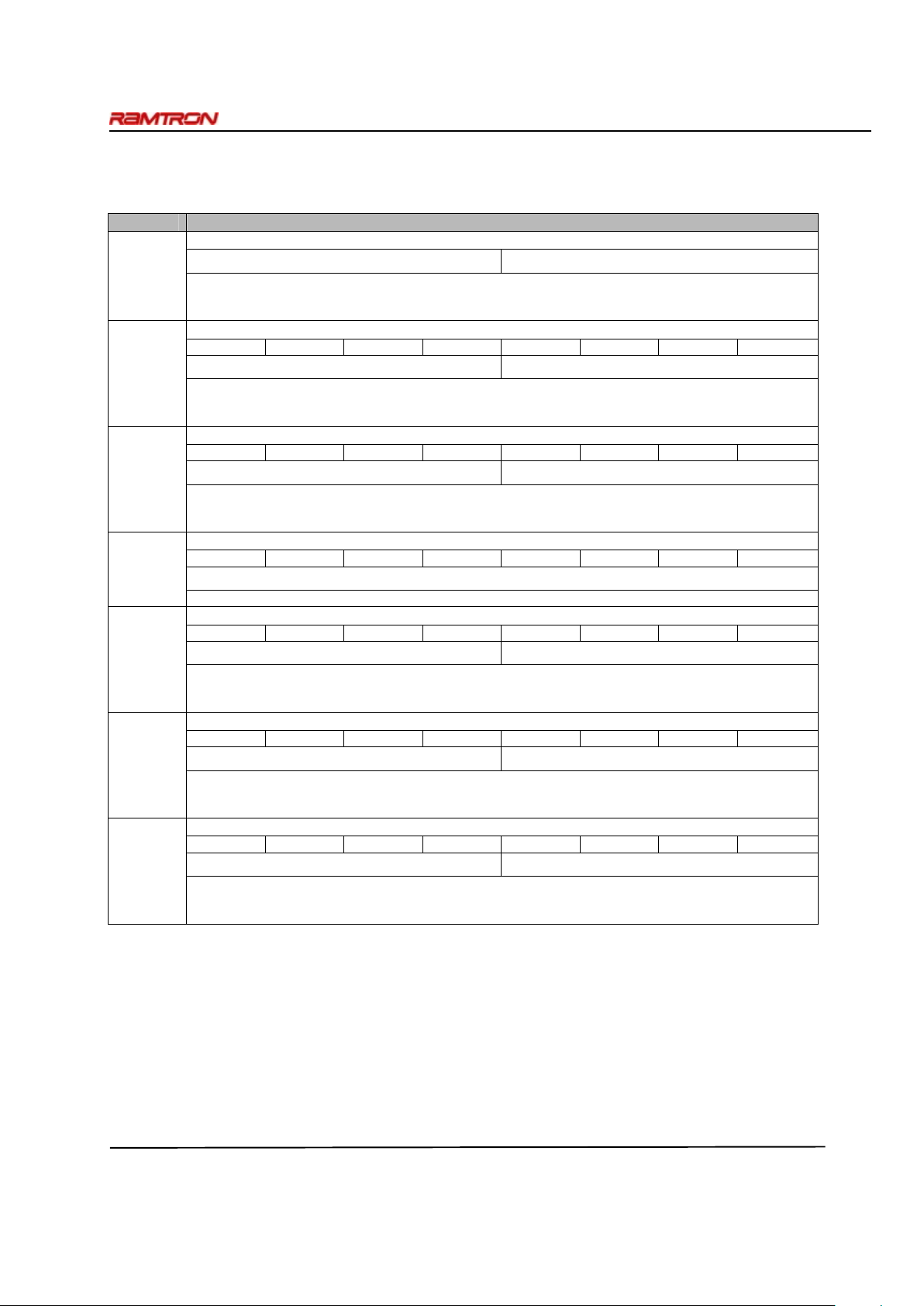
FM6124 Event Data Recorder
Rev. 1.0
April 2008 Page 27 of 53
Detailed Register Description
The following table contains the description of the Event Data Recorder and MCU Companion I2C registers.
Address Description
Event Data BCD Year 0x33
10s of Year Year
Contains the Event data Year in BCD format:
Upper Quartet contains 10s of Years
Lower Quartet contains unit of Years
Event Data BCD Month
D7 D6 D5 D4 D3 D2 D1 D0
0x32
10s of Month Month
Contains the Event data Month in BCD format:
Upper Quartet contains 10s of Month
Lower Quartet contains unit of Month
Event Data BCD Date
D7 D6 D5 D4 D3 D2 D1 D0
0x31
10s of Date Date
Contains the Event data Date in BCD format:
Upper quartet contains 10s of Date
Lower Quartet contains unit of Date
Event Data of Week
D7 D6 D5 D4 D3 D2 D1 D0
0x30
Contains Event Data Day of week
Event Data BCD Hours
D7 D6 D5 D4 D3 D2 D1 D0
0x2F
10s of Hours Hours
Contains the Event data hours in BCD format:
Upper quarters contains 10s of Hours
Lower Quartet contains unit of Hours
Event Data BCD Minutes
D7 D6 D5 D4 D3 D2 D1 D0
0x2E
10s of Minutes Minutes
Contains the Event data Minutes in BCD format:
Upper quarters contains 10s of Minutes
Lower Quartet contains unit of Minutes
Event Data BCD Seconds
D7 D6 D5 D4 D3 D2 D1 D0
0x2D
10s of Seconds Seconds
Contains the Event data seconds in BCD format:
Upper quarters contain 10s of seconds
Lower Quartet contains unit of seconds
Page 28
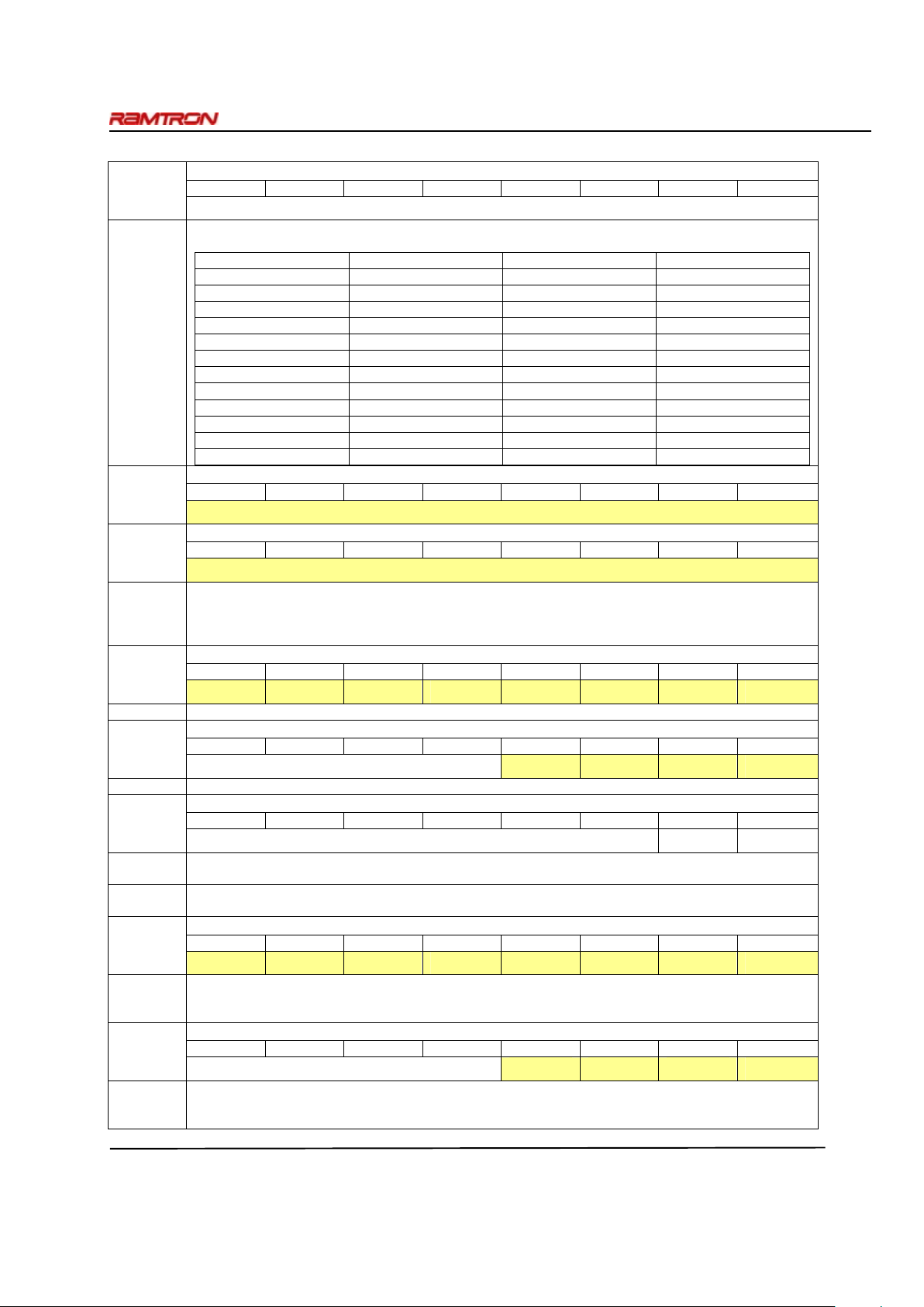
FM6124 Event Data Recorder
Rev. 1.0
April 2008 Page 28 of 53
Event Data Code
D7 D6 D5 D4 D3 D2 D1 D0
0x2C
Event Code[7:0]
Event Code
[7:0]
An Event code is associated with Each recorded event.
The table below shows the associat ion between the Events and their corresponding Event Code.
Event Event Code Event Event Code
EV_PIN0_FALL
0x08
EV_PIN6_FALL
0x14
EV_PIN0_RISE
0x09
EV_PIN6_RISE
0x15
EV_PIN1_FALL
0x0A
EV_PIN7_FALL
0x16
EV_PIN1_RISE
0x0B
EV_PIN7_RISE
0x17
EV_PIN2_FALL
0x0C
EV_PIN8_FALL
0x18
EV_PIN2_RISE
0x0D
EV_PIN8_RISE
0x19
EV_PIN3_FALL
0x0E
EV_PIN9_FALL
0x1A
EV_PIN3_RISE
0x0F
EV_PIN9_RISE
0x1B
EV_PIN4_FALL
0x10
EV_PIN10_FALL
0x1C
EV_PIN4_RISE
0x11
EV_PIN10_RISE
0x1D
EV_PIN5_FALL
0x12
EV_PIN11_FALL
0x1E
EV_PIN5_RISE
0x13
EV_PIN11_RISE
0x1F
Unread Events Counter MSB
D7 D6 D5 D4 D3 D2 D1 D0
0x2B
Number of Unread Even t Counter[15:8]
Unread Events Counter LSB
D7 D6 D5 D4 D3 D2 D1 D0
0x2A
Number of Unread Even t Counter[7:0]
# Unread
Event
Counter
[15:0]
This 16-bit register con t ain s the number of unread Event held in the FM 6124 Event Buffer F-RAM memory.
This value corresponds to the distance between WP and RP pointers.
A snapshot of the internal Unread Event Counter must be performed before reading this register.
This is done by writing 0x02 into the register located at address 27h
Pin Pass-Through B
D7 D6 D5 D4 D3 D2 D1 D0
0x29
P11 P10 P9 P8 P7 P6 P5 P4
P11-P4 Read Only: This register con t ains the Input pin logic level at the moment the snapshot was perfor med
Pin Pass-Through A
D7 D6 D5 D4 D3 D2 D1 D0
0x28
Reserved P3 P2 P1 P0
P3-P0 Read Only: This register contai ns the Input pin logic level at th e moment the snapshot was performed
Pin State – #Events Snapshot
D7 D6 D5 D4 D3 D2 D1 D0
0x27
Reserved NBEV SNAP
NBEV Write Only: Writing a 1 into the NBEVP will perform a snapshot read of the internal unread Events Counter
register and write the corresponding input logic level into the Register 2Ah and 2Bh
SNAP Write Only: Writing a 1 into the SNAP will perform a snapshot read of all 12 Input of the FM6124 and write the
corresponding input logic level into the Register 28h and 29h
Pin Event Enable B
D7 D6 D5 D4 D3 D2 D1 D0
0x26
P11 P10 P9 P8 P7 P6 P5 P4
P11-P4 Pin Event Enable
0: Event detection on the co rresponding input pin is disabled
1: Event detection on the co rresponding input pin is Activated
Pin Event Enable A
D7 D6 D5 D4 D3 D2 D1 D0
0x25
Reserved P3 P2 P1 P0
P3 – P0 Pin Event Enable
0: Event detection on the co rresponding input pin is disabled
1: Event detection on the co rresponding input pin is Activated
Page 29
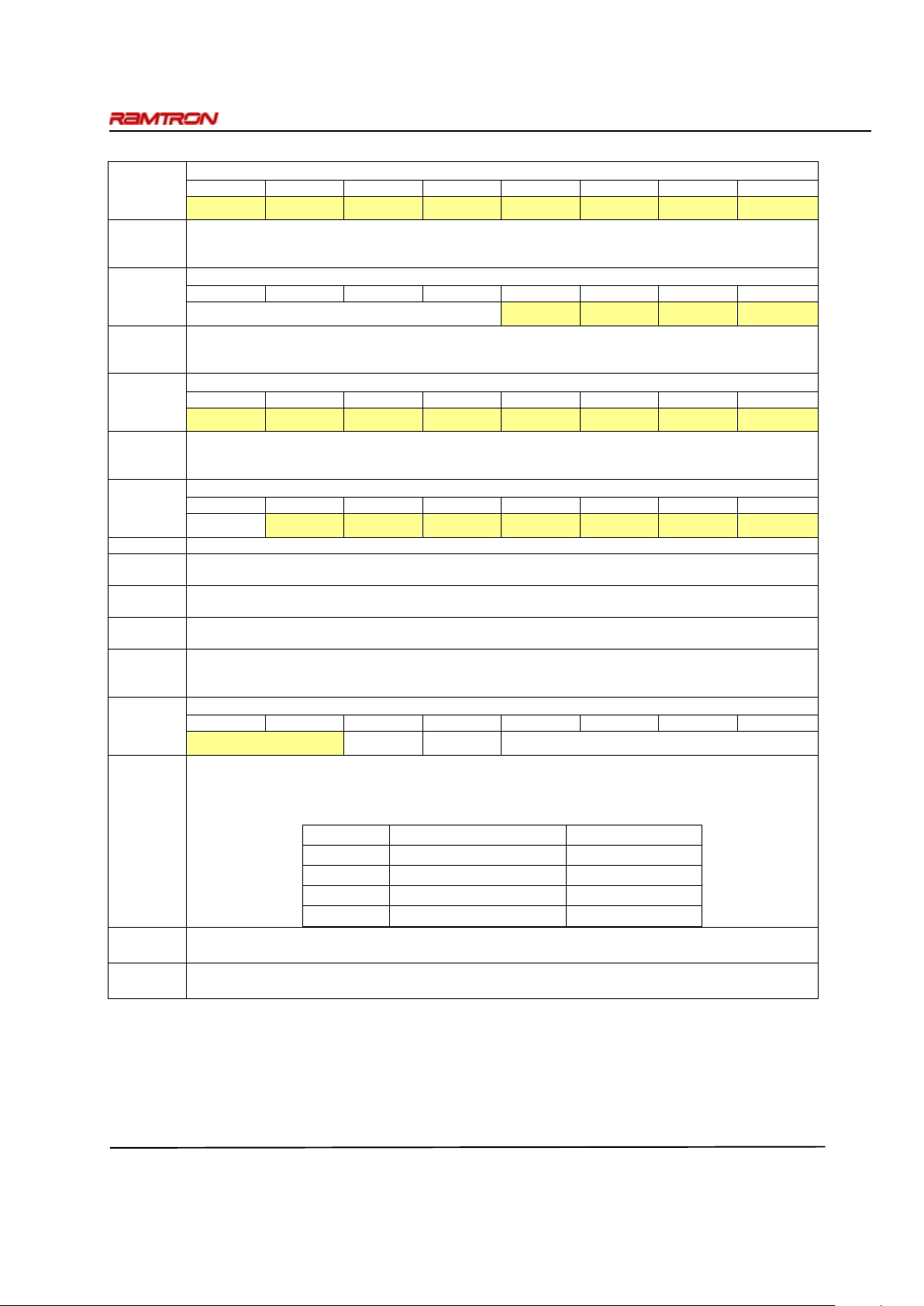
FM6124 Event Data Recorder
Rev. 1.0
April 2008 Page 29 of 53
Pin Event Rise/Fall A
D7 D6 D5 D4 D3 D2 D1 D0
0x24
P11 P10 P9 P8 P7 P6 P5 P4
Pin Event triggering condition
0: Pin will be triggered by a High to Low transition on the corresponding Input pin
1: Pin will be triggered by a Low to High transition on the corresponding Input pin
Pin Event Rise/Fall A
D7 D6 D5 D4 D3 D2 D1 D0
0x23
Reserved P3 P2 P1 P0
P3 – P0 Pin Event triggering condition
0: Pin will be triggered by a High to Low transition on the corresponding Input pin
1: Pin will be triggered by a Low to High transition on the corresponding Input pin
Pin Event Interrupt B
D7 D6 D5 D4 D3 D2 D1 D0
0x22
P11 P10 P9 P8 P7 P6 P5 P4
P11-P4 Pin Event Interrupt activate
0: the interrupt pin will not be activated when an Event will be detected on the corresponding input pin
1: The INT pin will be activated (Low) when a Event is detected on the corresponding Input pin
Pin Event interrupt A
D7 D6 D5 D4 D3 D2 D1 D0
0x21
CLEAR BF B75F B50F P3 P2 P1 P0
CLEAR Writing 1 to this Bit will deactivate the INT pin, when activated by a Pin Event interrupt
BF Buffer Full:
Writing 1 to this bit location will make the INT to become Active then the Buffer Full condition is met
B75F Buffer 75% Full:
Writing 1 to this bit location will make the INT to become Active then the Buffer gets 75% Full
B50F Buffer 50% Full:
Writing 1 to this bit location will make the INT to become Active then the Buffer gets 50% Full
P3 – P0 Pin Event Interrupt activate
0: the interrupt pin will not be activated when an Event will be detected on the corresponding input pin
1: The INT pin will be activated (Low) when a Event is detected on the corresponding Input pin
Event Recorder Control
D7 D6 D5 D4 D3 D2 D1 D0
0x20
EBUFSIZE[1:0] ERR READIR EDRCMD[3:0]
EBUFSIZE
[1:0]
Event Buffer and User F-RAM Sizes. Setting EBUFSIZE to a new value resets the Event Buffer.
Important: The user sho uld disable Event Recording while resetting the Event Buffer. Setting the
EBUFSIZE bits to a different value will reset all the Event Buffer.
EBUFSIZE Max number of Events User F-RAM size
00 4000 0
01 3000 8 KBytes
10 2000 16 Kbytes
11 1000 24 KBytes
ERR
Error bit (RO). User can read this bit to know if they have reach the end of the Event Buffer when
reading it. Writing ERR bit ha s no effect.
DIR
Event Buffer Read Direction. W hen set to ‘1’, Read pointer (RP) will be decremented (instead of
incremented) when an event has been read out of the Event Buffer.
Page 30
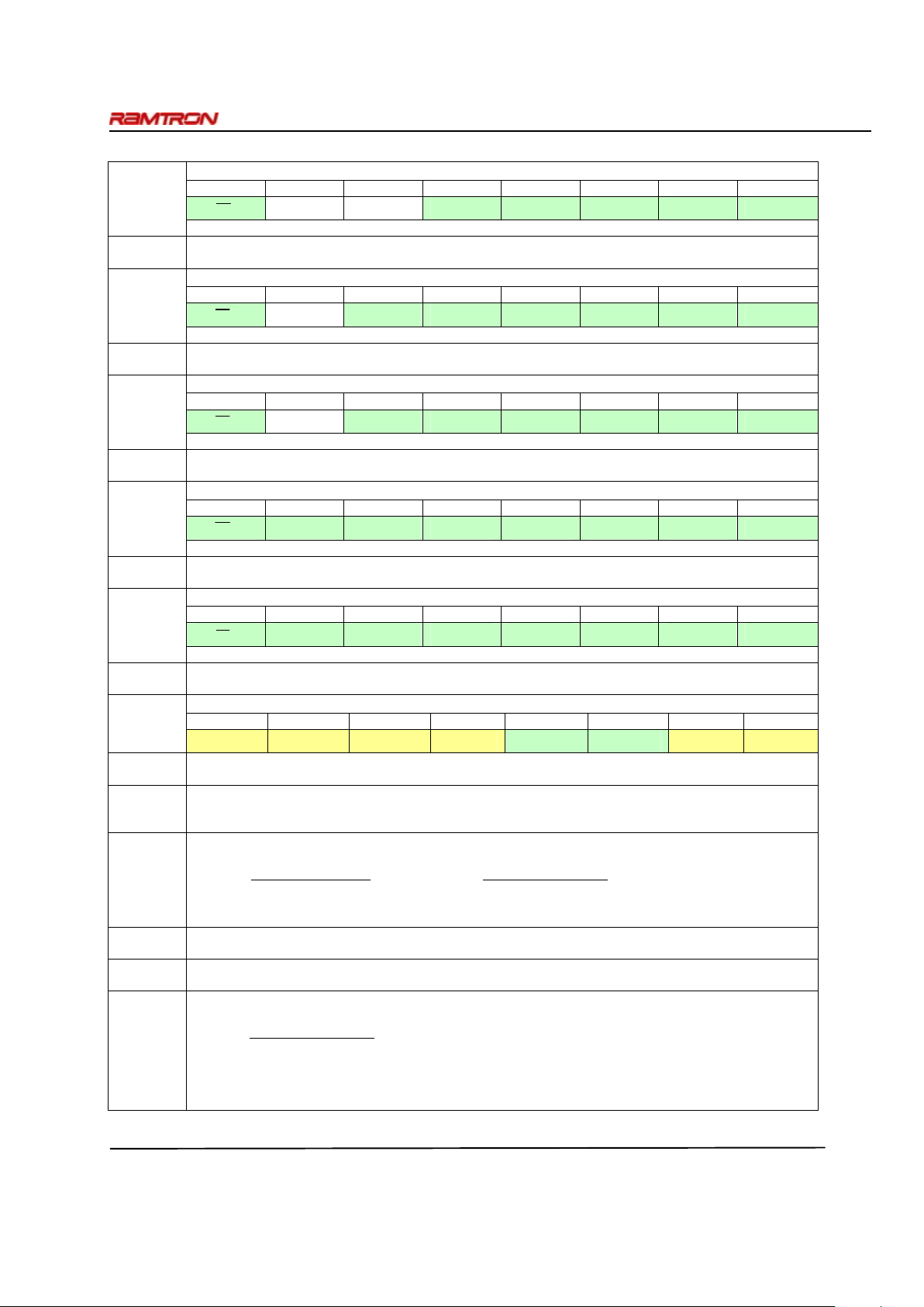
FM6124 Event Data Recorder
Rev. 1.0
April 2008 Page 30 of 53
Alarm – Month
D7 D6 D5 D4 D3 D2 D1 D0
0x1D
M 0 0 10 Month Month.3 Month.2 Month.1 Month.0
Contains the alarm value fo r t he month and the mask bit to select or deselect the Month val ue.
/M
Match. Setting this bit to 0 causes the Month value to be used in the alarm match logic. Setting th is bit to 1
causes the match circuit to ign ore the Month value. Battery-backed, read/write.
0x1C Alarm – Date
D7 D6 D5 D4 D3 D2 D1 D0
M 0 10 date.1 10 date.0 Date.3 Date.2 Date.1 Date.0
Contains the alarm value for the date and the mask bit to select or deselect the Date value.
/M Match: Setting this bit to 0 causes the Date value to be used in the alarm match logic. Setting this bit to 1 causes
the match circuit to ignore the Date value. Battery-backed, read/write.
0x1B Alarm – Hours
D7 D6 D5 D4 D3 D2 D1 D0
M 0 10 hours.1 10 hours.0 Hours.3 Hours2 Hours.1 Hours.0
Contains the alarm value for the hours and the mask bit to select or deselect the Hours value.
/M Match: Setting this bit to 0 causes the Hours value to be used in the alarm match logic. Setting this bit to 1 causes
the match circuit to ignore the Hours value. Battery-backed, read/write.
0x1A Alarm – Minutes
D7 D6 D5 D4 D3 D2 D1 D0
M 10 min.2 10 min.1 10 min.0 Min.3 Min.2 Min.1 Min.0
Contains the alarm value for t he minutes and the mask bit to sel ect or deselect the Minutes value
/M Match: Setting this bit to 0 causes the Minutes value to be used in the alarm match logic. Setting this bit to 1
causes the match circuit to ignore the Minutes value. Battery-backed, read/write.
0x19 Alarm – Seconds
D7 D6 D5 D4 D3 D2 D1 D0
M 10 sec.2 10 sec.1 10 sec.0 Seconds.3 Seconds.2 Seconds.1 Seconds.0
Contains the alarm value for the seconds and the mask bit to select or deselect the Seconds value.
/M Match: Setting this bit to 0 causes the Seconds value to be used in the alarm match logic. Setting this bit to 1
causes the match circuit to ign ore the Seconds value. Battery-backed, read/write.
0x18 Companion Control
D7 D6 D5 D4 D3 D2 D1 D0
SNL AL/SW F1 F0 VBC FC VTP1 VTP0
SNL Serial Number Lock: Setting to a ‘1’ makes registers 10h to 17h and SNL read-only. SNL cannot be cleared once
set to ‘1’. Nonvolatile, read/write.
AL/SW Alarm/Square Wave Select: When set to ‘1’, the alarm match drives the ACS pin as well as the AF flag. When
set to ‘0’, the selected Square Wave Freq will be driven on the ACS pin, and an alarm match only sets the AF
flag. Nonvolatile, read/write.
F(1:0) Square Wave Freq Select: These bits select t he frequency on the ACS pin when the CAL and AL/SW bits are
both ‘0’. Nonvolatile.
Setting F(1:0) Setting F(1:0)
1 Hz 00 (default) 4096 Hz 10
5
12 Hz
01 32768 Hz 11
VBC VBAK Charger Control: Setting VBC to ‘1’ (and FC=0) causes a 80 µA (1 mA if FC=1) trickle charge current to
be supplied on V
BAK
. Clearing VBC to ‘0’ disables the charge current. Battery-backed, read/write.
FC Fast Charge: Setting FC to ‘1’ (and VBC=1) causes a ~1 mA trickle charge current to be supplied on V
BAK
.
Clearing VBC to ‘0’ disables the charge curren t . Battery-backed, read/write.
VTP(1:0) VTP Select. These bits control the reset trip point for the low-VDD reset function. When VDD is below the
selected V
TP
voltage, the reset pin RSTB will drive low for the system. Nonvolatile, read/write.
Setting VTP(1:0)
2.60V 00 (factory default)
2.75V 01
2.9V 10
3.0V 11
Page 31
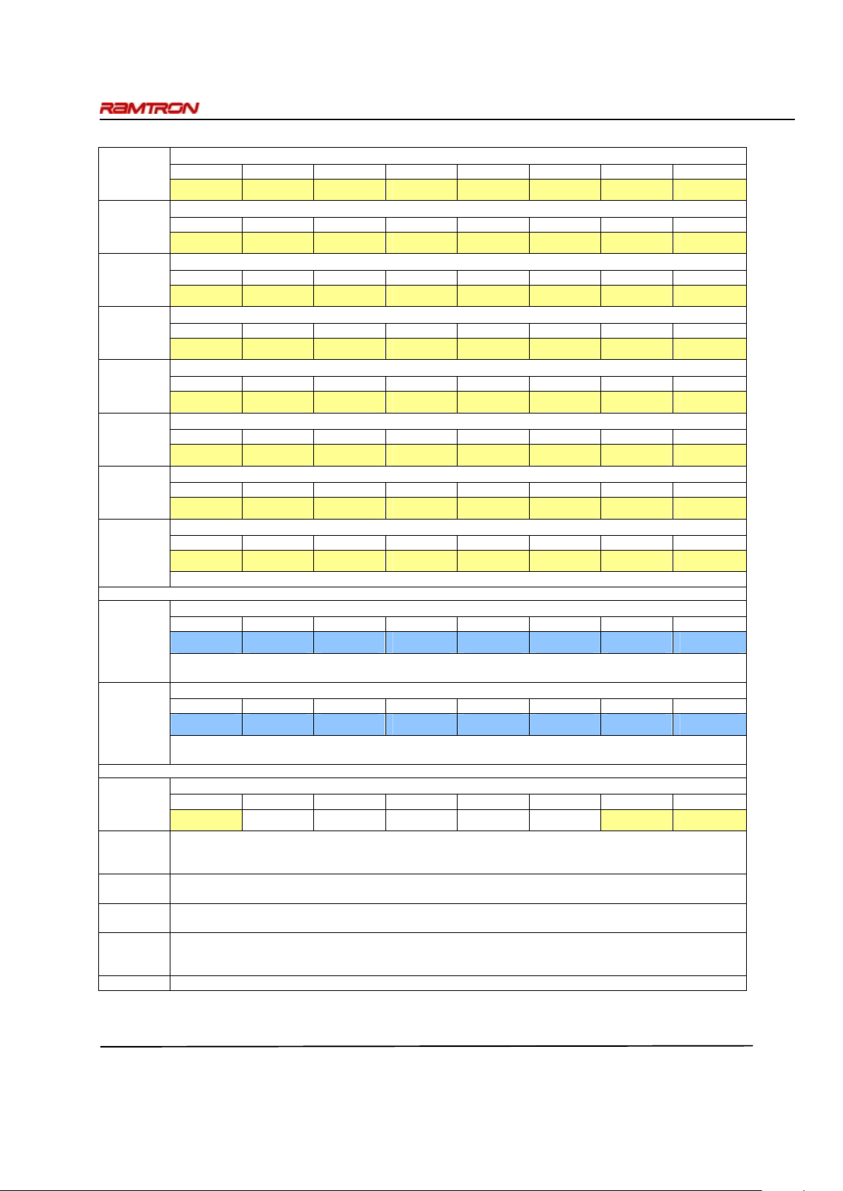
FM6124 Event Data Recorder
Rev. 1.0
April 2008 Page 31 of 53
0x17 Serial Number Byte 7
D7 D6 D5 D4 D3 D2 D1 D0
SN.63 SN.62 SN.61 SN.60 SN.59 SN.58 SN.57 SN.56
0x16 Serial Number Byte 6
D7 D6 D5 D4 D3 D2 D1 D0
SN.55 SN.54 SN.53 SN.52 SN.51 SN.50 SN.49 SN.48
0x15 Serial Number Byte 5
D7 D6 D5 D4 D3 D2 D1 D0
SN.47 SN.46 SN.45 SN.44 SN.43 SN.42 SN.41 SN.40
0x14 Serial Number Byte 4
D7 D6 D5 D4 D3 D2 D1 D0
SN.39 SN.38 SN.37 SN.36 SN.35 SN.34 SN.33 SN.32
0x13 Serial Number Byte 3
D7 D6 D5 D4 D3 D2 D1 D0
SN.31 SN.30 SN.29 SN.28 SN.27 SN.26 SN.25 SN.24
0x12 Serial Number Byte 2
D7 D6 D5 D4 D3 D2 D1 D0
SN.23 SN.22 SN.21 SN.20 SN.19 SN.18 SN.17 SN.16
0x11 Serial Number Byte 1
D7 D6 D5 D4 D3 D2 D1 D0
SN.15 SN.14 SN.13 SN.12 SN.11 SN.10 SN.9 SN.8
0x10 Serial Number Byte 0
D7 D6 D5 D4 D3 D2 D1 D0
SN.7 SN.6 SN.5 SN.4 SN.3 SN.2 SN.1 SN.0
All serial number bytes are read/write when SNL=0, read-only when SNL=1. Nonvo l at ile.
0x0F Event Counter Byte 1
D7 D6 D5 D4 D3 D2 D1 D0
EC.15 EC.14 EC.13 EC.12 EC.11 EC.10 EC.9 EC.8
Event Counter Byte 1. Increments on programmed edge event on CNT input. Nonvolatile when NVC=1,
Battery-backed when NVC=0, read/write.
0x0E Event Counter Byte 0
D7 D6 D5 D4 D3 D2 D1 D0
EC.7 EC.6 EC.5 EC.4 EC.3 EC.2 EC.1 EC.0
Event Counter Byte 0. Increments on programmed edge event on CNT input. Nonvolatile when NVC=1,
Battery-backed when NVC=0, read/write.
0x0D Event Counter Control
D7 D6 D5 D4 D3 D2 D1 D0
NVC - - - RC WC POLL CP
NVC Nonvolatile/Volatile Counter: Setting this bit to 1 makes the counter nonvolatile and counter operates only when
V
DD
is greater than VTP. Setting this bit to 0 makes the counter volatile, which allows counter operation under
V
BAK
or VDD power. Nonvolatile, read/write .
RC Read Counter. Setting this bit to 1 takes a snapshot of the two counter bytes allowing the system to read the
values without missing count events. The RC bit will be automatically cleared.
WC Write Counter. Setting this bit to a 1 allows the user to write the counter bytes. While WC=1, the counter is
blocked from count event s on the CNT pin. The WC bit must be cleared by the user to activate the counter.
POLL Polled Mode: When POLL=1, the CNT pin is sampled for 30µs every 125ms. If POLL is set, the NVC bit is
internally cleared and the CP bit is set to detect a rising edge. The RTC oscillator must be enabled (/OSCEN=0)
to operate in polled mode. When POLL=0, CNT pin is continuously active. Nonvolatile, read/write.
CP The CNT pin detects falling edges when CP = 0, rising edges when CP = 1. Nonvolatile, read/write.
Page 32
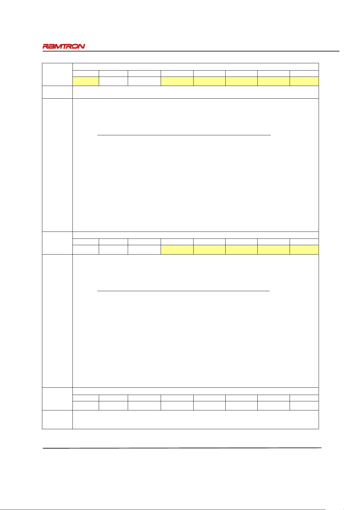
FM6124 Event Data Recorder
Rev. 1.0
April 2008 Page 32 of 53
0x0C Watchdog Control
D7 D6 D5 D4 D3 D2 D1 D0
WDE - - WDET4 WDET3 WDET2 WDET1 WDET0
WDE Watchdog Enable: When WDE=1, a watchdog timer fault will cause the RSTB signal to go active. When WDE
= 0 the timer runs but has no effect on the RSTB pin. Nonvolatile, read/write.
WDET(4:0) Watchdog EndTime: Sets the ending time for the watchdog window timer with 60 ms (min.) resolution. The
window timer allow independent leading and trailing edges (start and end of window) to be set. New watchdog
timeouts are loaded when the timer is restarted by writing the 1010b pattern to WR(3:0). To save power (disable
timer circuit), the EndTime may be set to all zeroes. Nonvolatile, read/write.
Watchdog EndTime
WDET4 WDET3 WDET2 WDET1 WDET0
Disables Timer 0 0 0 0 0
(min.) (max.)
60 ms 200 ms 0 0 0 0 1
120 ms 400 ms 0 0 0 1 0
180 ms 600 ms 0 0 0 1 1
. .
. .
. .
1200 ms 4000 ms 1 0 1 0 0
1260 ms 4200 ms 1 0 1 0 1
1320 ms 4400 ms 1 0 1 1 0
. .
. .
. .
1740 ms 5800 ms 1 1 1 0 1
1800 ms 6000 ms 1 1 1 1 0
1860 ms 6200 ms 1 1 1 1 1
0x0B Watchdog Control
D7 D6 D5 D4 D3 D2 D1 D0
- - - WDST4 WDST3 WDST2 WDST1 WDST0
WDST(4:0) Watchdog StartTime. Sets the starting time for the watchdog window timer with 25 ms (max.) resolution. The
window timer allow independent leading and trailing edges (start and end of window) to be set. New watchdog
timer settings are loaded when the timer is restarted by writing the 1010b pattern to WR(3:0). Nonvolatile,
read/write.
Watchdog StartTime
WDST4 WDST3 WDST2 WDST1 WDST0
0 ms (default) 0 0 0 0 0
(min.) (max.)
7.5 ms 25 ms 0 0 0 0 1
15.0 ms 50 ms 0 0 0 1 0
22.5 ms 75 ms 0 0 0 1 1
. .
. .
. .
150 ms 500 ms 1 0 1 0 0
157.5 ms 525 ms 1 0 1 0 1
165 ms 550 ms 1 0 1 1 0
. .
. .
. .
217.5 ms 725 ms 1 1 1 0 1
225 ms 750 ms 1 1 1 1 0
232.5 ms 775 ms 1 1 1 1 1
0x0A Watchdog Restart
D7 D6 D5 D4 D3 D2 D1 D0
- - - - WR3 WR2 WR1 WR0
WR(3:0) Watchdog Restart. Writing a pattern 1010b to WR(3:0) restarts the wat chdog timer. The upper nibble contents
do not affect this operation. Writing any pattern other than 1010b to WR3-0 has no effect on the watchdog.
Write-only.
Page 33
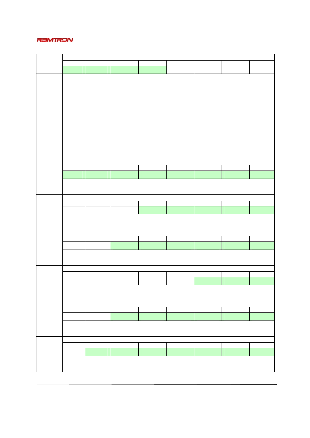
FM6124 Event Data Recorder
Rev. 1.0
April 2008 Page 33 of 53
0x09 Watchdog Flags
D7 D6 D5 D4 D3 D2 D1 D0
EWDF LWDF POR LB - - - -
EWDF Early Watchdog Timer Fault Flag: When a watchdog restart occurs too early (before the programmed watchdog
StartTime), the RSTB pin is driven low and this flag is set. It must be cleared by the user. Note that both EWDF
and POR could be set if both reset sources have occurred since the flags were cleared by the user. Batterybacked, read/write.
LWDF Late Watchdog Timer Fault Flag: When either a watchdog restart occurs too late (after the programmed
watchdog EndTime) or no restart occurs, the RSTB pin is driven low and this flag is set. It must be cleared by
the user. Note that both LWDF and POR could be set if both reset sources have occu rred since the flags were
cleared by the user. Battery-backed, read/ write.
POR
Power-On Reset: When the RSTB signal i s activated by V
DD
< VTP, the POR bit will be set to 1. A manual reset
will not set this flag. Note that one or both of the watchdog flags and the POR flag could be set if both reset
sources have occurred since the flags were cleared by the user. Battery-backed, read/write. (internally set, user
must clear bit)
LB Low Backup: If the V
BAK
source drops to a voltage l evel insufficient to operate the RTC/alarm when
V
DD<VBAK
, this bit will be set to ‘1’. All registers need to be re-initialized since the battery-backed register
values should be treated as unknown. The user should clear it to 0 when initializing the system. Battery-backed.
Read/Write (internally set, user must clear bit).
0x08
Timekeeping – Years
D7 D6 D5 D4 D3 D2 D1 D0
10 year.3 10 year.2 10 year.1 10 year.0 Year.3 Year.2 Year.1 Year.0
Contains the lower two BCD digits of the year. Lower nibble contains the value fo r years; upper nibble contains
the value for 10s of years. Each nibble operates from 0 to 9. The range for the register is 0-99. Battery-backed,
read/write.
0x07
Timekeeping – Months
D7 D6 D5 D4 D3 D2 D1 D0
0 0 0
10 Month Month.3 Month.2 Month.1 Month.0
Contains the BCD digits for the month. Lower nibble contains the lower digit and operates from 0 to 9; upper
nibble (one bit) contains the upper digit and operates from 0 to 1. The range for the register is 1-12. Batterybacked, read/write.
0x06
Timekeeping – Date of the month
D7 D6 D5 D4 D3 D2 D1 D0
0 0
10 date.1 10 date.0 Date.3 Date.2 Date.1 Date.0
Contains the BCD digits fo r the date of the month. Lower nibble contains the lower digit and operates from 0 to
9; upper nibble contains the upper digit and operates from 0 to 3. The range for the register is 1-31. Batterybacked, read/write.
0x05
Timekeeping – Day of the week
D7 D6 D5 D4 D3 D2 D1 D0
0 0 0 0 0
Day.2 Day.1 Day.0
Lower nibble contains a value that correlates to day of the week. Day of the week is a ring counter that counts
from 1 to 7 then returns to 1. The user must assign meaning to th e day value, as the day is not integrated with the
date. Battery-backed, read/write.
0x04
Timekeeping – Hours
D7 D6 D5 D4 D3 D2 D1 D0
0 0
10 hours.1 10 hours.0 Hours.3 Hours2 Hours.1 Hours.0
Contains the BCD value of hours in 24-hour format. Lower nibble contains the lower digit and operates from 0
to 9; upper nibble (two bits) contains the upper digit and operates from 0 to 2. The range for the register is 0-23.
Battery-backed, read/write.
0x03
Timekeeping – Minutes
D7 D6 D5 D4 D3 D2 D1 D0
0
10 min.2 10 min.1 10 min.0 Min.3 Min.2 Min.1 Min.0
Contains the BCD value of minutes. Lower nibble contains the lower digit and operates from 0 to 9; upper nibble
contains the upper minutes digit and operates from 0 to 5. The range for the register is 0-59. Battery-backed,
read/write.
Page 34
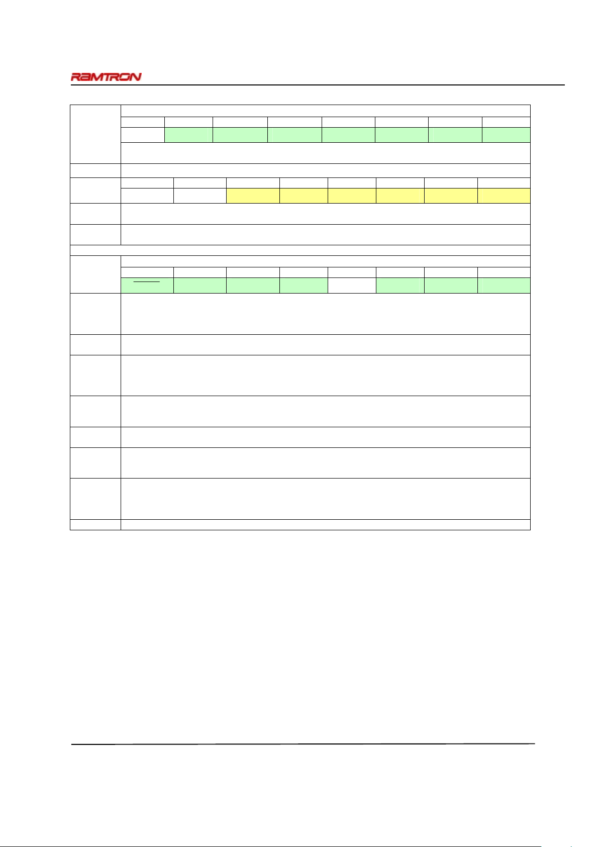
FM6124 Event Data Recorder
Rev. 1.0
April 2008 Page 34 of 53
0x02
Timekeeping – Seconds
D7 D6 D5 D4 D3 D2 D1 D0
0
10 sec.2 10 sec.1 10 sec.0 Seconds.3 Seconds.2 Seconds.1 Seconds.0
Contains the BCD value of seconds. Lower nibble contains the lower digit and operates from 0 to 9; upper nibble
contains the upper digit and operates from 0 to 5. The range for the register is 0-59. Battery-backed, read/write.
0x01
CAL/Control
D7 D6 D5 D4 D3 D2 D1 D0
- - CALS CAL.4 CAL.3 CAL.2 CAL.1 CAL.0
CALS Calibration Sign: Determines if the calibration adjustment is applied as an addition to or as a subtraction from the
time-base. This bit can be written only when CAL=1. Nonvolatile, read/write.
CAL.4-0 Calibration Code: These five bits control the calibration of the clock. These bits can be written only when
CAL=1. Nonvolatile, read/write.
0x00
RTC/Alarm Control
D7 D6 D5 D4 D3 D2 D1 D0
OSCEN AF CF AEN Reserved CAL W R
/OSCEN Oscillator Enable. When set to ‘1’, the oscillator is halted. When set to ‘0’, the oscillator runs. Disabling the
oscillator can save battery power during storage. On a power-up without a V
BAK
source or on a power-up after a
V
BAK
source has been applied, this bit is internally set to ‘1’, which turns off the oscillator. Battery-backed,
read/write.
AF Alarm Flag: This bit is set to 1 wh en the time and date match the values stored in the alarm registers with the
Match bit(s) = 0. The user must clear it to ‘0’. Battery-backed. (i nternally set, user must clear bit)
CF Century Overflow Flag: This bit is set to a 1 when the values in the years register overflows from 99 to 00. This
indicates a new century, such as going from 1999 to 2000 or 2099 to 2100. The user should record the new
century information as needed. The user must clear t he CF bit to ‘0’. Battery-backed. (internall y set, user must
clear bit)
AEN Alarm Enable: This bit enables the alarm function. When AEN is set (and CAL cleared), the ACS p in operates as
an active-low alarm. The state of the ACS pin is detailed in Table 2. Wh en AEN is cleared, no new alarm events
that set the AF bit will be generated. Clearing the AEN bit does not automatically clear AF. Battery-backed.
CAL Calibration Mode: When CAL is set to 1, the clock enters calibration mode. When CAL is set to 0, the clock
operates normally, and the ACS pin is controlled by the RTC alarm. Battery-backed, read/write.
W Write Time. Setting the W bit to 1 freezes updates of the user timekeeping registers. The user can then write
them with updated values. Setting the W bit to 0 causes the contents of the time registers to be transferred to the
timekeeping counters. Battery-backed, read/write.
R Read Time. Setting the R bit to ‘1’ copies a static image of the timekeeping core and places it into the user
registers. The user can then read them with out concerns over changing values cau si ng system errors. The R bit
going from 0 to 1 causes the timekeeping capture, so the bit must be returned to 0 prior to reading again. Batterybacked, read/write.
Reserved Reserved bit s. Do not use. Should remain set to 0.
Page 35

FM6124 Event Data Recorder
Rev. 1.0
April 2008 Page 35 of 53
Electrical Specifications
Absolute Maximum Ratings
Symbol Description Ratings
VDD Power Supply Voltage with respect to VSS -1.0V to +3.6V
VIN Voltage on any signal pin with respect to VSS -1.0V to +5.0V and
V
IN
< VDD+1.0V
V
BAK
Backup Supply Voltage -1.0V to +4.5V
T
STG
Storage Temperature
-55°C to + 125°C
T
LEAD
Lead Temperature (Soldering, 10 seconds)
300° C
V
ESD
Electrostatic Discharge Voltage
- Human Body Model
(JEDEC Std JESD22-A114-E)
- Charged Device Model (JEDEC Std JESD22-C101-C)
- Machine Model
(JEDEC Std JESD22-A115-A)
TBD
TBD
TBD
Package Moisture Sensitivity Level MSL-3
Stresses above those listed under Absolute Maximum Ratings may cause permanent damage to the device. This is a stress rating
only, and th e function al opera tion of t he devic e at th ese or an y other co nditi ons ab ove those li sted i n the op eration al secti on of this
specification is not implied. Exposure to absolute maximum ratings conditions for extended periods may affect device reliability.
DC Operating Conditions (
TA = -40° C to + 85° C, VDD = 3.0V to 3.6V unless otherwise specified)
Symbol Parameter Min Typ Max Units Notes
VDD Main Power Supply 3.0 - 3.6 V 1
IDD V
DD
Supply Current (VBC=0) mA
ISB Standby Current
Trickle Charger Off
(VBC=0)
50
µA
3
V
BAK
RTC Backup Voltage 2.0 3.0 3.6 V 4
I
BAK
RTC Backup Curr ent 1
µA
5
I
BAKTC
Trickle Charge Current with V
BAK
=0V
Fast Charge Off (FC = 0)
Fast Charge On (FC = 1)
50
200
200
2500
µA
µA
6
V
TP0
VDD Trip Point Voltage for MCU companion &
RTC, VTP(1:0) = 00b
2.55 2.6 2.70 V 7
V
TP1
VDD Trip Point Voltage for MCU companion &
RTC, VTP(1:0) = 01b
2.70 2.75 2.85 V 7
V
TP2
VDD Trip Point Voltage for MCU companion &
RTC, VTP(1:0) = 10b
2.80 2.9 2.97 V 7
V
TP3
VDD Trip Point Voltage for MCU companion &
RTC, VTP(1:0) = 11b
2.93 3.0 3.13 V 7
V
RST
V
BAK
> V
BAK
min
V
BAK
< V
BAK
min
0
1.6
V V
VSW Battery Switchover Voltage 2.0 2.7 V
ILI Input Leakage Current TBD
µA
ILO Output Leakage Current TBD
µA
VIL Input Low Voltage
All inputs except as listed below
CNT battery-backed (V
DD
< VSW)
CNT (V
DD
> VSW)
-0.3
-0.3
-0.3
0.3 V
DD
0.5
0.8
V
V
V
VIH Input High Voltage
All inputs except as listed below
CNT battery-backed (V
DD
< VSW)
CNT V
DD
> VSW
PFI
0.7 V
DD
V
BAK
– 0.5
0.7 V
DD
-
V
DD
+ 0.3
V
BAK
+ 0.3
V
DD
+ 0.3
V
DD
+ 0.3
V
V
V
V
Continued >>
Page 36

FM6124 Event Data Recorder
Rev. 1.0
April 2008 Page 36 of 53
DC Operating Conditions, continued
(TA = -40° C to + 85° C, VDD = 3.0V to 3.6V unless otherwise specified)
Symbol Parameter
Min Typ Max Units Notes
VOL Output Low Voltage @ IOL = 3 mA - 0.4 V
VOH Output High Voltage
(PFO) @ I
OH
= -2 mA
VDD – 0.8
-
V
R
RSTB
Pull-up resistance for RSTB inactive 50 400
KΩ
V
PFI
Power Fail Input Reference Voltage 1.475 1.50 1.525 V
V
HYS
Power Fail Input (PFI) Hysteresis (Rising) - 100 mV
Notes
1.
Full complete operation. Supervisory circuits, RTC, etc operate to lower voltages as specified.
2.
All inputs at VSS or V
DD,
static. Trickle charger off (VBC=0).
3.
The VBAK trickle charger automatically regulates the maximum voltage on this pin for capacitor backup applicat io ns.
4.
V
BAK
= 3.0V, VDD < VSW, oscillator running, CNT at VBAK.
5.
V
BAK
will source current when trickle charge is enabled (VBC bit=1), VDD > V
BAK
, and V
BAK
< V
BAK
max.
6.
This is the VDD supply current contributed by enabling the trickle charger circu i t, and does not account for I
BAKTC
.
7.
The min i mum VDD to guarantee the level of RSTB remai ns a valid VOL level.
AC Parameters
(TA = -40° C to + 85° C, VDD = 3.0V to 3.6V, CL = 100 pF unless otherwise specified)
Symbol Parameter Min Max Units Notes
f
SCL
SCL Clock Frequency 0 100 kHz
t
LOW
Clock Low Period 4.7
µs
t
HIGH
Clock High Period 4.0
µs
tAA SCL Low to SDA Data Out Valid 3
µs
t
BUF
Bus Free Before New Transmission 4.7
µs
t
HD:STA
Start Condition Hold Time 4.0
µs
t
SU:STA
Start Condition Setup for Repeated Start 4.7
µs
t
HD:DAT
Data In Hold Time 0 ns
t
SU:DAT
Data In Setup Time TBD ns
tR Input Rise Time TBD ns 1
tF Input Fall Time TBD ns 1
t
SU:STO
Stop Condition Setup Time 4.0
µs
tDH Data Output Hold
(from SCL @ VIL)
0 ns
All SCL specifications as well as start and stop conditions apply to both read and write operations.
Supervisor Timing (TA = -40° C to + 85° C, VDD = 3.0V to 3.6V)
Symbol Parameter Min Max Units Notes
t
RPW
RSTB Pulse Width (active low time) 30 100 ms
t
RNR
RSTB Response Time to VDD<VTP (noise filter) 7 25
µs
1
tVR V
DD
Rise Time 50 -
µs/V
1,2
tVF V
DD
Fall Time 100 -
µs/V
1,2
t
WDST
Watchdog StartTime 0.3*t
DOG1
t
DOG1
ms 3
t
WDET
Watchdog EndTime t
DOG2
3.3*t
DOG2
ms 3
f
CNT
Frequency of Event Counter 0 TBD kHz
Notes
1 This parameter is characterized but not tested.
2 Slope measured at any point on V
DD
waveform.
3 t
DOG1
is the programmed StartTime an d t
DOG2
is the programmed EndTime in registers 0B h and 0Ch, VDD > VTP, and t
RPU
satisfied. The StartTime has a resolution of 25ms. The EndTime has a resolution of 60ms.
4 The RSTB pin will drive low for this amount of time after the internal reset circuit is activated due to a watchdog, low
voltage, or manual reset event.
Page 37
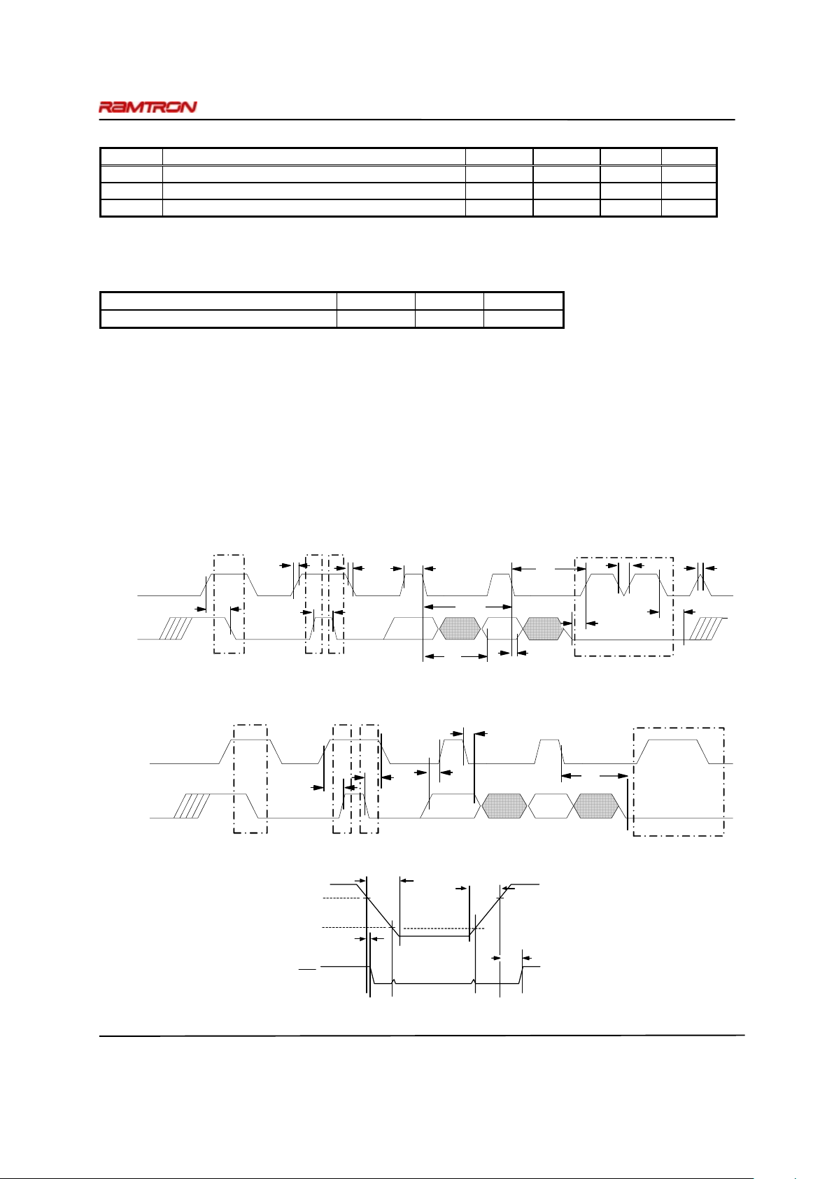
FM6124 Event Data Recorder
Rev. 1.0
April 2008 Page 37 of 53
Capacitance (TA = 25° C, f=1.0 MHz, VDD = 3.0V)
Symbol Parameter Typ Max Units Notes
CIO Input/Output Capacitance - 20 pF 1
C
XTL
X1, X2 Crystal pin Capacitance 25 - pF 1, 2
C
CNT
Max. Allowable Capacitance on CNT (polled mode) - 100 pF
Notes
1 This parameter is characterized but not tested.
2 The crystal attached to th e X1/X2 pins must be rated as 12.5pF .
Data Retention (V
DD
= 3.0V to 3.6V)
Parameter Min Units Notes
Data Retention 10 Years
AC Test Conditions
Input Pulse Levels 10% and 90% of V
DD
Input Rise and Fall Times 5 ns
Input and Output Timing Levels 0.5 V
DD
Output Load Capacitance 100 pF
Diagram Notes
All start and stop timing parameters apply to both read and write cycles. Clock specifications are identical for read
and write cycles. Write timing parameters apply to slave address, word address, and write data bits. Functional
relationships are illustrated in the re levant data sheet sections. These diagrams illustrate the timing parameters onl y.
Read Bus Timing
t
SU:STA
Start
t
R
`
t
F
Stop Start
t
BUF
t
HIGH
1/f
SCL
t
LOW
t
SP
t
SP
Acknowledge
t
HD:DAT
t
SU:DAT
t
AA
t
DH
SCL
SDA
Write Bus Timing
t
SU:STO
Start
Stop Start Acknowledge
t
AA
t
HD:DAT
t
HD:STA
t
SU:DAT
SCL
SDA
RSTB Timing
VDD
VTP
VRST
RST
t
RPU
t
VF
t
RNR
t
VR
Page 38

FM6124 Event Data Recorder
Rev. 1.0
April 2008 Page 38 of 53
FM6124 Interface Code Example
The following C code provides an example of basic interface to the FM6124 using Ramtron’s High Performance
VRS51L2070 (8051-based) MCU.
////////////////////////////////////////////////////////////////////////////////
//
// $Date: 2008-03-10 13:04:43 -0400 (Mon, 10 Mar 2008) $
// $Rev: 250 $
// $Author: smalo $
// $fm6124_basic_example_vrs2070.c $
//
////////////////////////////////////////////////////////////////////////////////
//
// Description: This file contains code examples for a
// Host MCU (Ramtron VRS51L2070) communicating with an
// Event Data Recorder (Ramtron FM6124 EDR).
// The host MCU is connected to the FM6124 with an I2C interface.
// The compiler used for this example is SDCC 2.7.0
//
// Remarks: For the purpose of this example, the device selection bits
// of the FM6124 (A0 and A1) are fixed to 1.
// See global variable "g_uiI2CDevSelect".
//
// Copyright (C) 2008 Ramtron International Corporation
//
////////////////////////////////////////////////////////////////////////////////
#include <malloc.h>
#include "VRS51L2070_SDCC.h" // VRS51L2070 registers definitions
#include "fm6124.h" // FM6124 registers definitions
////////////////////////////////////////////////////////////////////////////////
// Function Prototypes
////////////////////////////////////////////////////////////////////////////////
// I2C Init functions
void InitI2C();
rbool IsI2CSlaveReady(ruint8 a_uiSlaveId);
// FM6124 Access functions
ruint8 FM6124ReadReg(ruint8 a_uiRegAddr);
rbool FM6124WriteReg(ruint8 a_uiRegAddr, ruint8 a_uiRegValue);
rbool FM6124WriteRTC(struct SBCDDate *a_poDate);
ruint8 FM6124ReadFRAM(ruint16 a_uiFramAddr);
rbool FM6124WriteFRAM(ruint16 a_uiFramAddr, ruint8 a_uiValue);
rbool FM6124ReadEventAtRP(struct SEvent *a_poEvent);
rbool FM6124StreamEventsAtRP(ruint8* a_puiEvents, ruint8 a_uiNbEvents);
// Utility functions
void Delay(ruint16 a_uiDelayMs);
rbool CreateEventsP5(ruint16 a_uiNbEvents);
////////////////////////////////////////////////////////////////////////////////
// Global variables
////////////////////////////////////////////////////////////////////////////////
// Fix device selection bits (A0 and A1) to 1.
// These are bits 2:1 of the first byte of an I2C transaction.
const ruint8 g_uiI2CDevSelect = 0x03 << 1;
Page 39

FM6124 Event Data Recorder
Rev. 1.0
April 2008 Page 39 of 53
////////////////////////////////////////////////////////////////////////////////
// Function: main
// Description: main function of the program
// Parameters: None
// Return value: int: Error Code
// Remarks: For the purpose of this example, the return values
// of functions are not verified. In a real application,
// return values should be verified in order to make sure that
// any all operations have completed successfully.
////////////////////////////////////////////////////////////////////////////////
int
main()
{
__idata ruint8 l_uiDataByte = 0x00;
__idata ruint16 l_uiNbEvents = 0x0000;
__xdata struct SBCDDate l_oRTCValue;
__xdata struct SEvent l_oEvent;
__xdata ruint8* l_puiEvents = NULL;
/////////////
// INIT Phase
// Initialize I2C interface, making sure FM6124 is responding.
InitI2C();
// Reset RTC to a defined value
l_oRTCValue.uiSeconds = 0x00;
l_oRTCValue.uiMinutes = 0x01;
l_oRTCValue.uiHours = 0x02;
l_oRTCValue.uiDay = 0x03;
l_oRTCValue.uiDate = 0x10;
l_oRTCValue.uiMonth = 0x09;
l_oRTCValue.uiYear = 0x07;
FM6124WriteRTC(&l_oRTCValue);
// Configure Event Buffer to 1000 Events
FM6124WriteReg(EDR_REG_BUFFER_CTRL, EDR_BC_CMD_EB_SIZE | EDR_BC_VAR_3000_EVENTS);
Delay(1);
FM6124WriteReg(EDR_REG_BUFFER_CTRL, EDR_BC_CMD_EB_SIZE | EDR_BC_VAR_1000_EVENTS);
// Make sure FM6124 has enough time to setup the new Event Buffer (100us required)
Delay(1);
///////////////////
// F-RAM Write/Read
// Write a Byte into the F-RAM at address 0x0000
FM6124WriteFRAM(0x0000, 0xBD);
// Read a Byte of Data in the F-RAM at address 0x0000
l_uiDataByte = FM6124ReadFRAM(0x0000);
////////////////
// Create Events
// Enable Event Recording of Digital Input 4-11 (Rising Edges)
FM6124WriteReg(EDR_REG_PIN_RF_B, 0xFF);
FM6124WriteReg(EDR_REG_PIN_EE_B, 0xFF);
// Make sure FM6124 has enough time to enable Event Recording (100us required)
Delay(1);
// Disable Event Recording
FM6124WriteReg(EDR_REG_PIN_EE_B, 0x00);
//////////////
// Read Events
// Read Number of Events (Number of Events between RP and WP)
FM6124WriteReg(EDR_REG_PIN_SNAP, 0x02);
l_uiNbEvents = FM6124ReadReg(EDR_REG_EVENT_COUNT_MSB);
l_uiNbEvents <<= 8;
l_uiNbEvents |= FM6124ReadReg(EDR_REG_EVENT_COUNT_LSB);
// Read newest event:
// 1- Move RP to the last event
FM6124WriteReg(EDR_REG_BUFFER_CTRL, EDR_BC_CMD_LAST);
// 2- Read Event
FM6124ReadEventAtRP(&l_oEvent);
Page 40

FM6124 Event Data Recorder
Rev. 1.0
April 2008 Page 40 of 53
// Read 5 oldest Events by streaming:
// 1- Move RP to first event:
FM6124WriteReg(EDR_REG_BUFFER_CTRL, EDR_BC_CMD_FIRST);
// 2- Allocate memory for 5 Events
l_puiEvents = malloc(5 * sizeof(struct SEvent));
// 3- Stream 5 Events
if (l_puiEvents != NULL)
{
FM6124StreamEventsAtRP(l_puiEvents, 5);
}
// Final note: to "see" the result of this example, it can be executed with
// Ramtron's Versaware JTAG debugger. At this point, you can verify that all operations
// were completed successfully by looking at the memory content of the Host MCU
// running this program.
if (l_uiDataByte != 0xBD)
{
return 1;
}
if (l_uiNbEvents != 10)
{
return 2;
}
return 0;
}
////////////////////////////////////////////////////////////////////////////////
// Function: InitI2C
// Description: Enable and initialize I2C in MASTER Mode
// Parameters: None
// Return value: None
// Remarks: None
////////////////////////////////////////////////////////////////////////////////
void
InitI2C()
{
// Enable I2C module
PERIPHEN1 |= 0x20;
// Init the transmit portion of the I2CRXTX buffer
// I2C Master
I2CCONFIG = 0x01;
I2CIDCFG = 0x41;
// I2C Comm Speed = 96.15 Khz (Max speed of FM6124 is 100kHz)
I2CTIMING = 0x0C;
// Make sure FM6124 is responding
while(!IsI2CSlaveReady(I2C_ID_EDR))
{
Delay(1000);
}
}
Page 41

FM6124 Event Data Recorder
Rev. 1.0
April 2008 Page 41 of 53
////////////////////////////////////////////////////////////////////////////////
// Function: IsI2CSlaveReady
// Description: Check if an I2C Slave module is ready by issuing a write
// operation. We abort the write operation after the I2C Id
// is transmitted. If the I2C Id is Acknowledged, it means
// that the I2C slave module is ready.
// Parameters: ruint8 a_uiSlaveId: Id of the Slave Module to check
// Return value: rbool: RFALSE = Slave is not ready
// RTRUE = Slave is ready
// Remarks: None
////////////////////////////////////////////////////////////////////////////////
rbool
IsI2CSlaveReady(ruint8 a_uiSlaveId)
{
// Send Write command to Slave Module
I2CRXTX = a_uiSlaveId | g_uiI2CDevSelect | IC2_WRITE;
// Wait for TX Buffer to be empty
while(!(I2CSTATUS & 0x01));
// Wait for I2C to be Idle
// This will generate a STOP and cancel the Write operation
while(!(I2CSTATUS & 0x08));
if (I2CSTATUS & 0x40)
{
// No ACK received, Slave Module is not ready
return RFALSE;
}
return RTRUE;
}
////////////////////////////////////////////////////////////////////////////////
// Function: FM6124ReadReg
// Description: Read a Register of the FM6124
// Parameters: ruint8 a_uiRegAddr
// Return value: ruint8: Value of the register read
// Remarks: To Read a register on the I2C, we first need to "fake"
// a write operation in order to send the register address to the
// slave module.
////////////////////////////////////////////////////////////////////////////////
ruint8
FM6124ReadReg(ruint8 a_uiRegAddr)
{
ruint8 l_uiValue = 0x00;
// Make sure I2C is Idle
while(!(I2CSTATUS & 0x08));
// Wait for TX Buffer to be empty
while((I2CSTATUS & 0x01) == 0);
// Dummy Read to clear the I2CRXAVF
l_uiValue = I2CRXTX;
// "Fake" write operation to send the register address we want to read
I2CRXTX = I2C_ID_EDR | g_uiI2CDevSelect | IC2_WRITE;
// Wait for TX Buffer to be empty
while((I2CSTATUS & 0x01) == 0);
// Make sure we received an ACK.
if (I2CSTATUS & 0xC0)
{
return 0xFF;
}
// Send Read Address
I2CRXTX = a_uiRegAddr;
// Wait for I2C to be Idle and generate a STOP
while(!(I2CSTATUS & 0x08));
// Make sure we received an ACK.
if (I2CSTATUS & 0xC0)
{
return 0xFF;
}
Page 42

FM6124 Event Data Recorder
Rev. 1.0
April 2008 Page 42 of 53
// READ OPERATION
// Dummy Read to clear the I2CRXAVF
l_uiValue = I2CRXTX;
// Make sure we will ACK the Data we will receive
I2CCONFIG &= 0xFD;
// Now, send the Read command to the FM6124
I2CRXTX = I2C_ID_EDR | g_uiI2CDevSelect | IC2_READ;
// Wait for Data to comeback
while(!(I2CSTATUS & 0x02));
l_uiValue = I2CRXTX;
// Stop the transaction
I2CCONFIG |= 0x02;
// Wait for I2C to be Idle and generate a STOP
while(!(I2CSTATUS & 0x08));
return l_uiValue;
}
////////////////////////////////////////////////////////////////////////////////
// Function: FM6124WriteReg
// Description: Write a Register of the FM6124
// Parameters: ruint8 a_uiRegAddr
// ruint8 a_uiRegValue
// Return value: rbool: RTRUE = Operation Ok.
// Remarks: None
////////////////////////////////////////////////////////////////////////////////
rbool
FM6124WriteReg(ruint8 a_uiRegAddr, ruint8 a_uiRegValue)
{
// Make sure I2C is Idle
while(!(I2CSTATUS & 0x08));
// Wait for TX Buffer to be empty
while((I2CSTATUS & 0x01) == 0);
// Send Write command
I2CRXTX = I2C_ID_EDR | g_uiI2CDevSelect | IC2_WRITE;
// Wait for TX Buffer to be empty
while((I2CSTATUS & 0x01) == 0);
// Make sure we received an ACK and that there was no error during transfer
if (I2CSTATUS & 0xC0)
{
return RFALSE;
}
// Send Write Address
I2CRXTX = a_uiRegAddr;
// Wait for TX Buffer to be empty
while((I2CSTATUS & 0x01) == 0);
// Make sure we received an ACK and that there was no error during transfer
if (I2CSTATUS & 0xC0)
{
return RFALSE;
}
// Send Write Data
I2CRXTX = a_uiRegValue;
// Wait for TX Buffer to be empty
while((I2CSTATUS & 0x01) == 0);
// Make sure we received an ACK and that there was no error during transfer
if (I2CSTATUS & 0xC0)
{
return RFALSE;
}
// Wait for I2C to be Idle, this will generate a STOP
while(!(I2CSTATUS & 0x08));
// Make sure we received an ACK and that there was no error during transfer
if (I2CSTATUS & 0xC0)
{
return RFALSE;
}
return RTRUE;
}
Page 43

FM6124 Event Data Recorder
Rev. 1.0
April 2008 Page 43 of 53
////////////////////////////////////////////////////////////////////////////////
// Function: FM6124WriteRTC
// Description: Write all registers of the RTC of the FM6124.
// Parameters: struct SBCDDate *a_poDate: Date to be written
// Return value: rbool: RFALSE = Error during read operation.
// Remarks: None
////////////////////////////////////////////////////////////////////////////////
rbool
FM6124WriteRTC(struct SBCDDate *a_poDate)
{
ruint8 l_uiCounter = 0x00;
ruint8 *l_puiDateElement = NULL;
ruint8 l_uiRTCRegValue = 0x00;
// First, we need to read the RTC register of the FM6124
l_uiRTCRegValue = FM6124ReadReg(EDR_REG_RTC);
// Next, we need to enable the writing of the RTC
l_uiRTCRegValue |= 0x02;
FM6124WriteReg(EDR_REG_RTC, l_uiRTCRegValue);
// Make sure I2C is Idle
while(!(I2CSTATUS & 0x08));
// Wait for TX Buffer to be empty
while((I2CSTATUS & 0x01) == 0);
// Send Write command to Slave Module
I2CRXTX = I2C_ID_EDR | g_uiI2CDevSelect | IC2_WRITE;
// Wait for TX Buffer to be empty
while((I2CSTATUS & 0x01) == 0);
// Make sure we received an ACK and that there was no error during transfer
if (I2CSTATUS & 0xC0)
{
return RFALSE;
}
// Send Write Address
I2CRXTX = EDR_REG_RTC_SECS;
// Wait for TX Buffer to be empty
while((I2CSTATUS & 0x01) == 0);
// Make sure we received an ACK and that there was no error during transfer
if (I2CSTATUS & 0xC0)
{
return RFALSE;
}
// Write RTC Data
l_puiDateElement = &(a_poDate->uiSeconds);
for (l_uiCounter = 0; l_uiCounter < 7; l_uiCounter++)
{
I2CRXTX = *l_puiDateElement;
// Wait for TX Buffer to be empty
while((I2CSTATUS & 0x01) == 0);
// Make sure we received an ACK and that there was no error during transfer
if (I2CSTATUS & 0xC0)
{
return RFALSE;
}
l_puiDateElement++;
}
// Wait for I2C to be Idle, This will generate a STOP
while(!(I2CSTATUS & 0x08));
// Now, we need to restore the original RTC register value.
// Clear "W" bit
// Make sure Oscillator is running: Clear /OSCEN bit
l_uiRTCRegValue &= 0x7D;
FM6124WriteReg(EDR_REG_RTC, l_uiRTCRegValue);
return RTRUE;
}
Page 44

FM6124 Event Data Recorder
Rev. 1.0
April 2008 Page 44 of 53
////////////////////////////////////////////////////////////////////////////////
// Function: FM6124ReadFRAM
// Description: Read 1 byte of Data in the F-RAM of the FM6124
// Parameters: ruint16 a_uiFramAddr
// Return value: ruint8: Byte read
// Remarks: To Read a data on the I2C, we first need to "fake"
// a write operation in order to send the memory address to the
// slave module.
////////////////////////////////////////////////////////////////////////////////
ruint8
FM6124ReadFRAM(ruint16 a_uiFramAddr)
{
ruint8 l_uiDataRead;
// Make sure I2C is Idle
while(!(I2CSTATUS & 0x08));
// Wait for TX Buffer to be empty
while((I2CSTATUS & 0x01) == 0);
// Dummy Read to clear the I2CRXAVF
l_uiDataRead = I2CRXTX;
// Send Write command to FM6124
I2CRXTX = I2C_ID_FM | g_uiI2CDevSelect | IC2_WRITE;
// Wait for TX Buffer to be empty
while((I2CSTATUS & 0x01) == 0);
// Make sure we received an ACK and that there was no error during transfer
if (I2CSTATUS & 0xC0)
{
return 0xFF;
}
// Send Read Address, 8 MSB
I2CRXTX = (a_uiFramAddr >> 8) & 0xFF;
// Wait for TX Buffer to be empty
while((I2CSTATUS & 0x01) == 0);
// Make sure we received an ACK and that there was no error during transfer
if (I2CSTATUS & 0xC0)
{
return 0xFF;
}
// Send Read Address, 8 LSB
I2CRXTX = a_uiFramAddr & 0xFF;
// Wait for I2C to be Idle, This will generate a STOP
while(!(I2CSTATUS & 0x08));
// Make sure we received an ACK and that there was no error during transfer
if (I2CSTATUS & 0xC0)
{
return 0xFF;
}
// Now, send the Read command to the FM6124
I2CRXTX = I2C_ID_FM | g_uiI2CDevSelect | IC2_READ;
// Wait for Data to comeback
while(!(I2CSTATUS & 0x02));
l_uiDataRead = I2CRXTX;
// Stop the transaction
I2CCONFIG |= 0x02;
// Wait for I2C to be Idle, This will generate a STOP
while(!(I2CSTATUS & 0x08));
// Make sure we received an ACK and that there was no error during transfer
if (I2CSTATUS & 0xC0)
{
return 0xFF;
}
return l_uiDataRead;
}
Page 45

FM6124 Event Data Recorder
Rev. 1.0
April 2008 Page 45 of 53
////////////////////////////////////////////////////////////////////////////////
// Function: FM6124WriteFRAM
// Description: Write 1 byte of Data into the FRAM of the FM6124
// Parameters: ruint16 a_uiFramAddr
// ruint8 a_uiValue
// Return value: rbool: RTRUE = Operation successful.
// Remarks: None
////////////////////////////////////////////////////////////////////////////////
rbool
FM6124WriteFRAM(ruint16 a_uiFramAddr, ruint8 a_uiValue)
{
// Make sure I2C is Idle
while(!(I2CSTATUS & 0x08));
// Wait for TX Buffer to be empty
while((I2CSTATUS & 0x01) == 0);
// Send Write command to FM6124
I2CRXTX = I2C_ID_FM | g_uiI2CDevSelect | IC2_WRITE;
// Wait for TX Buffer to be empty
while((I2CSTATUS & 0x01) == 0);
// Make sure we received an ACK and that there was no error during transfer
if (I2CSTATUS & 0xC0)
{
return RFALSE;
}
// Send Write Address, 8 MSB
I2CRXTX = (a_uiFramAddr >> 8) & 0xFF;
// Wait for TX Buffer to be empty
while((I2CSTATUS & 0x01) == 0);
// Make sure we received an ACK and that there was no error during transfer
if (I2CSTATUS & 0xC0)
{
return RFALSE;
}
// Send Write Address, 8 LSB
I2CRXTX = a_uiFramAddr & 0xFF;
// Wait for TX Buffer to be empty
while((I2CSTATUS & 0x01) == 0);
// Make sure we received an ACK and that there was no error during transfer
if (I2CSTATUS & 0xC0)
{
return RFALSE;
}
// Send 1 Byte of Data
I2CRXTX = a_uiValue;
// Wait for TX Buffer to be empty
while((I2CSTATUS & 0x01) == 0);
// Make sure we received an ACK and that there was no error during transfer
if (I2CSTATUS & 0xC0)
{
return RFALSE;
}
// Wait for I2C to be Idle, This will generate a STOP
while(!(I2CSTATUS & 0x08));
// Make sure we received an ACK and that there was no error during transfer
if (I2CSTATUS & 0xC0)
{
return RFALSE;
}
return RTRUE;
}
Page 46

FM6124 Event Data Recorder
Rev. 1.0
April 2008 Page 46 of 53
////////////////////////////////////////////////////////////////////////////////
// Function: FM6124ReadEventAtRP
// Description: Read Event pointed by the current position of RP (Read Pointer)
// Parameters: struct SEvent *a_poEvent: Pointer to a SEvent, which
// will receive the Event's values.
// Return value: rbool: RTRUE = Read Ok.
// Remarks: None
////////////////////////////////////////////////////////////////////////////////
rbool
FM6124ReadEventAtRP(struct SEvent *a_poEvent)
{
// First, we need to indicate the FM6124 that we want to read an Event
FM6124WriteReg(EDR_REG_BUFFER_CTRL, EDR_BC_CMD_GET);
// Make sure I2C is Idle
while(!(I2CSTATUS & 0x08));
// Wait for TX Buffer to be empty
while((I2CSTATUS & 0x01) == 0);
// Dummy Read, to clear the I2CRxAv flag.
a_poEvent->uiEventCode = I2CRXTX;
// "Fake" write operation to send the register address we want to read
I2CRXTX = I2C_ID_EDR | g_uiI2CDevSelect | IC2_WRITE;
// Wait for TX Buffer to be empty
while((I2CSTATUS & 0x01) == 0);
// Make sure we received an ACK and that there was no error during transfer
if (I2CSTATUS & 0xC0)
{
return RFALSE;
}
// Send Read Address
I2CRXTX = EDR_REG_EVT_CODE;
// Wait for I2C to be Idle and generate a STOP
while(!(I2CSTATUS & 0x08));
// Make sure we received an ACK and that there was no error during transfer
if (I2CSTATUS & 0xC0)
{
return RFALSE;
}
// READ EVENT
// Dummy Read to clear the I2CRXAVF
a_poEvent->uiEventCode = I2CRXTX;
// Make sure we will ACK the Data we will receive
I2CCONFIG &= 0xFD;
// Now, send the Read command to the Slave ER
I2CRXTX = I2C_ID_EDR | g_uiI2CDevSelect | IC2_READ;
while(!(I2CSTATUS & 0x02));
a_poEvent->uiEventCode = I2CRXTX;
while(!(I2CSTATUS & 0x02));
a_poEvent->oBCDDate.uiSeconds = I2CRXTX;
while(!(I2CSTATUS & 0x02));
a_poEvent->oBCDDate.uiMinutes = I2CRXTX;
while(!(I2CSTATUS & 0x02));
a_poEvent->oBCDDate.uiHours = I2CRXTX;
while(!(I2CSTATUS & 0x02));
a_poEvent->oBCDDate.uiDay = I2CRXTX;
while(!(I2CSTATUS & 0x02));
a_poEvent->oBCDDate.uiDate = I2CRXTX;
while(!(I2CSTATUS & 0x02));
a_poEvent->oBCDDate.uiMonth = I2CRXTX;
while(!(I2CSTATUS & 0x02));
a_poEvent->oBCDDate.uiYear = I2CRXTX;
// Stop the transaction
I2CCONFIG |= 0x02;
// Wait for I2C to be Idle and generate a STOP
while(!(I2CSTATUS & 0x08));
return RTRUE;
}
Page 47

FM6124 Event Data Recorder
Rev. 1.0
April 2008 Page 47 of 53
////////////////////////////////////////////////////////////////////////////////
// Function: FM6124StreamEventsAtRP
// Description: Read x events by Streaming, starting at RP
// Parameters:
// Return value: rbool: RTRUE = Read Ok.
// Remarks: User is responsible of:
// 1- Making sure a_puiEvents has enough space to contain
// a_uiNbEvents events.
// 2- There is at least a_uiNbEvents in the Event Buffer of the
// FM6124.
////////////////////////////////////////////////////////////////////////////////
rbool
FM6124StreamEventsAtRP(ruint8* a_puiEvents, ruint8 a_uiNbEvents)
{
ruint8 l_uiCurEvent = 0x00;
ruint8 l_uiCurData = 0x00;
rbool l_bEventFF = RFALSE;
ruint8* l_puiVufPrt = a_puiEvents;
// Send STEAM command to the FM6124
FM6124WriteReg(EDR_REG_BUFFER_CTRL, EDR_BC_CMD_STREAM);
// Make sure I2C is Idle
while(!(I2CSTATUS & 0x08));
// Wait for TX Buffer to be empty
while((I2CSTATUS & 0x01) == 0);
// Dummy Read, to clear the I2CRxAv flag.
*a_puiEvents = I2CRXTX;
// "Fake" write operation to send the register address we want to read
I2CRXTX = I2C_ID_EDR | g_uiI2CDevSelect | IC2_WRITE;
// Wait for TX Buffer to be empty
while((I2CSTATUS & 0x01) == 0);
// Make sure we received an ACK and that there was no error during transfer
if (I2CSTATUS & 0xC0)
{
return RFALSE;
} // Send Read Address
I2CRXTX = EDR_REG_EVT_CODE;
while(!(I2CSTATUS & 0x08)); // Wait for I2C to be Idle: STOP
// Make sure we received an ACK and that there was no error during transfer
if (I2CSTATUS & 0xC0)
{
return RFALSE;
}
// Start the Event Streaming by sending the read command.
// Make sure we will ACK the Data we will receive
I2CCONFIG &= 0xFD;
// Dummy Read to clear the I2CRXAVF
*a_puiEvents = I2CRXTX;
// Now, send the Read command
I2CRXTX = I2C_ID_EDR | g_uiI2CDevSelect | IC2_READ;
l_uiCurEvent = 0;
l_bEventFF = RFALSE;
while ((l_bEventFF == RFALSE) &&
(l_uiCurEvent < a_uiNbEvents))
{
l_bEventFF = RTRUE;
// Receive 8 bytes per Event
for (l_uiCurData = 0; l_uiCurData < 8; l_uiCurData++)
{
// Wait for Data to comeback
while(!(I2CSTATUS & 0x02));
*l_puiVufPrt = I2CRXTX;
if (*l_puiVufPrt != 0xFF)
{
l_bEventFF = RFALSE;
}
l_puiVufPrt++;
}
l_uiCurEvent++;
Page 48

FM6124 Event Data Recorder
Rev. 1.0
April 2008 Page 48 of 53
}
// Stop the streaming
I2CCONFIG |= 0x02;
// Wait for I2C to be Idle and generate a STOP
while(!(I2CSTATUS & 0x08));
if ((l_uiCurEvent != a_uiNbEvents) ||
(l_bEventFF == RTRUE))
{
return RFALSE;
}
return RTRUE;
}
////////////////////////////////////////////////////////////////////////////////
// Function: Delay
// Description: Wait x milliseconds
// Parameters: ruint16 uiDelayMs: Delay, in ms
// Return value: None
// Remarks: Calibrated for VRS51L2070 running at 40MHZ.
// This function uses Timer0
////////////////////////////////////////////////////////////////////////////////
void
Delay(ruint16 a_uiDelayMs)
{
ruint16 l_uiDelayLoop = a_uiDelayMs;
// Enable Timer 0
PERIPHEN1 |= 0x01;
while ( l_uiDelayLoop > 0)
{
T0T1CLKCFG &= 0xF0;
// Timer0 reload value for 1ms @ 40Mhz
TH0 = 0x63;
TL0 = 0xC0;
// Start Timer0
T0CON = 0x04;
// Wait for timer0 overflow
while (!(T0CON & 0x80));
// Stop Timer 0
T0CON = 0x00;
l_uiDelayLoop--;
}
// Disable Timer0
PERIPHEN1 & 0xFE;
}
Page 49

FM6124 Event Data Recorder
Rev. 1.0
April 2008 Page 49 of 53
Include File:
////////////////////////////////////////////////////////////////////////////////
//
// $Date: 2008-03-10 13:04:27 -0400 (Mon, 10 Mar 2008) $
// $Rev: 249 $
// $Author: smalo $
// $HeadURL: file:…fm6124.h $
//
////////////////////////////////////////////////////////////////////////////////
//
// Description: This file contains C functions declarations and defines
// for the Ramtron Event Data Recorder (EDR) FM6124.
//
// Remarks:
//
// Copyright (C) 2008 Ramtron International Corporation
//
////////////////////////////////////////////////////////////////////////////////
#ifndef FM6124_H
#define FM6124_H
////////////////////////////////////////////////////////////////////////////////
// Include and defines
////////////////////////////////////////////////////////////////////////////////
#include "ramtron_types.h" // Ramtron basic type definitions
// I2C Ids of the FM6124
// The first byte of any I2C transaction contains the Slave Module Id.
// Bits 7:1 are used for the Id
// Bit 0 indicates if the command is Read (1) or a Write (0)
#define I2C_ID_EDR 0xA0
#define I2C_ID_FM 0xD0
#define IC2_WRITE 0x00
#define IC2_READ 0x01
////////////////////////////////////////////////////////////////////////////////
// Type Definitions
////////////////////////////////////////////////////////////////////////////////
typedef struct SBCDDate
{
ruint8 uiSeconds;
ruint8 uiMinutes;
ruint8 uiHours;
ruint8 uiDay;
ruint8 uiDate;
ruint8 uiMonth;
ruint8 uiYear;
};
typedef struct SBCDAlarmDate
{
ruint8 uiSeconds;
ruint8 uiMinutes;
ruint8 uiHours;
ruint8 uiDate;
ruint8 uiMonth;
};
typedef struct SEvent
{
ruint8 uiEventCode;
struct SBCDDate oBCDDate;
};
Page 50

FM6124 Event Data Recorder
Rev. 1.0
April 2008 Page 50 of 53
////////////////////////////////////////////////////////////////////////////////
// FM6124 Enums
////////////////////////////////////////////////////////////////////////////////
enum EventType
{
EV_PIN0_FALL = 0x08,
EV_PIN0_RISE = 0x09,
EV_PIN1_FALL = 0x0A,
EV_PIN1_RISE = 0x0B,
EV_PIN2_FALL = 0x0C,
EV_PIN2_RISE = 0x0D,
EV_PIN3_FALL = 0x0E,
EV_PIN3_RISE = 0x0F,
EV_PIN4_FALL = 0x10,
EV_PIN4_RISE = 0x11,
EV_PIN5_FALL = 0x12,
EV_PIN5_RISE = 0x13,
EV_PIN6_FALL = 0x14,
EV_PIN6_RISE = 0x15,
EV_PIN7_FALL = 0x16,
EV_PIN7_RISE = 0x17,
EV_PIN8_FALL = 0x18,
EV_PIN8_RISE = 0x19,
EV_PIN9_FALL = 0x1A,
EV_PIN9_RISE = 0x1B,
EV_PIN10_FALL = 0x1C,
EV_PIN10_RISE = 0x1D,
EV_PIN11_FALL = 0x1E,
EV_PIN11_RISE = 0x1F,
};
// FM6124 Event Data Recorder (EDR) Registers
enum EDRRegisters
{
EDR_REG_RTC = 0x00,
EDR_REG_CAL = 0x01,
EDR_REG_RTC_SECS = 0x02,
EDR_REG_RTC_MINS = 0x03,
EDR_REG_RTC_HOURS = 0x04,
EDR_REG_RTC_DAY = 0x05,
EDR_REG_RTC_DATE = 0x06,
EDR_REG_RTC_MONTH = 0x07,
EDR_REG_RTC_YEAR = 0x08,
EDR_REG_WD_FLAGS = 0x09,
EDR_REG_WD_RESTART = 0x0A,
EDR_REG_WD_CTRL0 = 0x0B,
EDR_REG_WD_CTRL1 = 0x0C,
EDR_REG_CNT_CTRL = 0x0D,
EDR_REG_CNT_LSB = 0x0E,
EDR_REG_CNT_MSB = 0x0F,
EDR_REG_SN_BYTE0 = 0x10,
EDR_REG_SN_BYTE1 = 0x11,
EDR_REG_SN_BYTE2 = 0x12,
EDR_REG_SN_BYTE3 = 0x13,
EDR_REG_SN_BYTE4 = 0x14,
EDR_REG_SN_BYTE5 = 0x15,
EDR_REG_SN_BYTE6 = 0x16,
EDR_REG_SN_BYTE7 = 0x17,
EDR_REG_CC = 0x18,
EDR_REG_ALM_SECS = 0x19,
EDR_REG_ALM_MINS = 0x1A,
EDR_REG_ALM_HOURS = 0x1B,
EDR_REG_ALM_DATE = 0x1C,
EDR_REG_ALM_MONTH = 0x1D,
EDR_REG_BUFFER_CTRL = 0x20,
Page 51

FM6124 Event Data Recorder
Rev. 1.0
April 2008 Page 51 of 53
EDR_REG_PIN_INT_A = 0x21,
EDR_REG_PIN_INT_B = 0x22,
EDR_REG_PIN_RF_A = 0x23,
EDR_REG_PIN_RF_B = 0x24,
EDR_REG_PIN_EE_A = 0x25,
EDR_REG_PIN_EE_B = 0x26,
EDR_REG_PIN_SNAP = 0x27,
EDR_REG_PIN_STATE_A = 0x28,
EDR_REG_PIN_STATE_B = 0x29,
EDR_REG_EVENT_COUNT_LSB = 0x2A,
EDR_REG_EVENT_COUNT_MSB = 0x2B,
EDR_REG_EVT_CODE = 0x2C,
EDR_REG_EVT_SECS = 0x2D,
EDR_REG_EVT_MINS = 0x2E,
EDR_REG_EVT_HOURS = 0x2F,
EDR_REG_EVT_DAY = 0x30,
EDR_REG_EVT_DATE = 0x31,
EDR_REG_EVT_MONTH = 0x32,
EDR_REG_EVT_YEAR = 0x33,
};
// Buffer Control Register Bits
enum
{
EDR_BC_CMD_BITS = 0x0F,
EDR_BC_DIR_BIT = 0x10,
EDR_BC_ERR_BIT = 0x20,
EDR_BC_VAR_BITS = 0xC0,
EDR_BC_CMD_NOTHING = 0x0,
EDR_BC_CMD_GET = 0x1,
EDR_BC_CMD_GET_KEEP = 0x2,
EDR_BC_CMD_STREAM = 0x3,
EDR_BC_CMD_STREAM_KEEP = 0x4,
EDR_BC_CMD_SKIP = 0x5,
EDR_BC_CMD_FIRST = 0x6,
EDR_BC_CMD_LAST = 0x7,
EDR_BC_CMD_EB_SIZE = 0x8,
EDR_BC_VAR_4000_EVENTS = 0x00,
EDR_BC_VAR_3000_EVENTS = 0x40,
EDR_BC_VAR_2000_EVENTS = 0x80,
EDR_BC_VAR_1000_EVENTS = 0xC0,
};
// EDR_REG_PIN_INT_A Bits
enum
{
EDR_PIN_INT_A_BHF_BIT = 0x10,
EDR_PIN_INT_A_B75F_BIT = 0x20,
EDR_PIN_INT_A_BF_BIT = 0x40,
EDR_PIN_INT_A_CLEAR_BIT = 0x80,
EDR_PIN_INT_A_CLEAR_BIT_MASK = 0x7F,
};
#endif // FM6124_H
Page 52
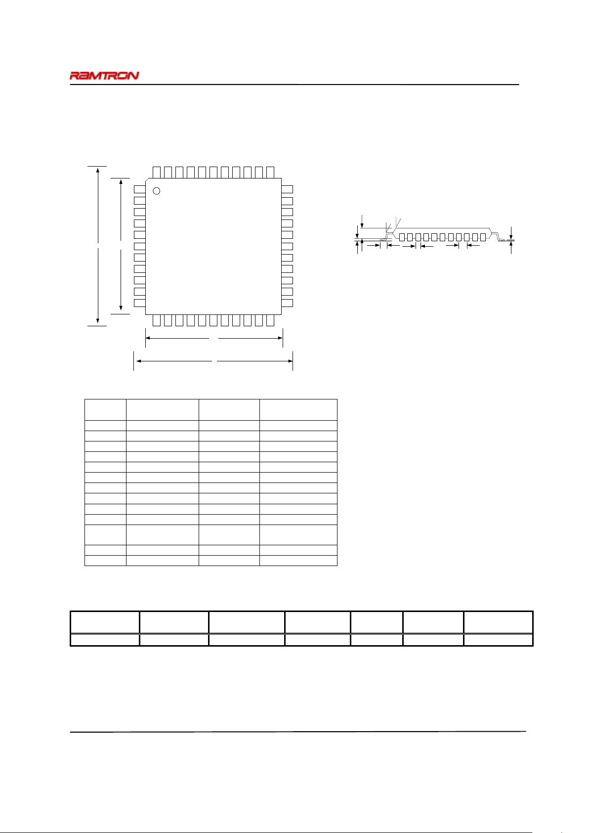
FM6124 Event Data Recorder
Rev. 1.0
April 2008 Page 52 of 53
MECHANICAL DRAWING
QFP-44 Package
A2
A1
c
e
b
E1
D1
D
E
L
d3
d1
d2
1
2
3
4
5
6
7
8
9
10
11
3435363738394041424344
22
12 13 14 15 16 17
18 19
20 21
23
24
25
26
27
28
29
30
31
32
33
TABLE 1) DIMENSIONS OF QFP-44 PACKAGES
Symbol Description
Dimension
(mm)
Tolerance
(mm, º) / Notes
D
Footprint 13.2 +/- 0.25
D1
Body size 10 +/- 0.10
E Footprint
13.2 +/- 0.25
E1 Body size
10 +/- 0.10
A1 Stand-off 0.25 Max
A2
Body thickness 2.00
L Lead Length 0.88 +0.15 / -0.10
b Lead width 0.35 +/- 0.05
c L/C thickness 0.17 Max
e Lead pitch 0.8
d1
Body edge
angle
10º
d2 Lead angle 6º +/- 4º
d3 Lead angle 0º to 7º
ORDERING INFORMATION
Device
Number
Total F-RAM
Memory Size
Recorder Events
F-RAM
User Data
F-RAM Size
Package Voltage Temperature
Range
FM6124-QG 32KB 1000 - 4000 0 – 24KB QFP-44 3.0V to 3.6V -40°C to +85°C
Page 53

FM6124 Event Data Recorder
Rev. 1.0
April 2008 Page 53 of 53
Revision History
Revision
Date
Summary
1.0 04/11/2008 Initial release.
 Loading...