

Page 1

Product Preview
FM3808
256Kb Bytewide FRAM w/Real-Time Clock
Features
256K bit Ferroelectric NonVolatile RAM
• Organized as 32,752 x 8 bits
• High Endurance 100 Billion (10
• 10 year Data Retention
• NoDelay™ Writes
• 70 ns Access Time/ 130 ns Cycle Time
• Built-in Low V
Protection
DD
Real-Time Clock/Calendar Function
• Clock Registers in Top 16 bytes of Address Space
• Backup Power from External Capacitor or Battery
• Tracks Seconds through Centuries in BCD Format
• Tracks Leap Years through 2099
• Runs from a 32.768 kHz Timekeeping Crystal
Description
The FM3808 combines a 256Kb FRAM array with a
real-time clock and a system supervisor function. The
timekeeping function is driven by a user supplied
32.768 kHz crystal. It maintains time and date
settings in the a bsence of system power through the
user’s choice of backup power source – either
capacitor or battery. In either case data in the memory
array does not depend on the backup source, it
remains nonvolatile in FRAM. In addition to
timekeeping, the FM3808 includes a system
supervisor to manage low V
a watchdog timer function. A programmable interrupt
output pin allows the user to select the supervisor
functions and the polarity of the signal.
Both the FRAM array and the timekeeping function
are accessed through the memory interface. The
upper 16-address locations of the memory space are
allocated to the timekeeping registers rather than to
memory. The FRAM array provides data retention
for 10 years in the absence of system power, and is
not dependent on the backup power source used for
the clock. This eliminates system concerns over data
loss in a traditional battery-backed RAM solution. In
addition, clock and supervisor control settings are
implemented in FRAM rather than battery-backed
RAM, making them more dependable. The FM3808
offers guaranteed operation over an industrial
temperature range of -40°C to +85°C.
DD
11
) Read/Writes
power conditions and
Pin Configuration
A11
A9
A8
A13
WE
VBAK
INT
VDD
X1
X2
A14
A12
A7
A6
A5
A4 A3
FM3808-70-T 70 ns access, 32-pin TSOP
FM3808DK DIP module development kit
Documentation for the DIP module development kit is
provided separately.
System Supervisor Function
• Programmable Clock/Calendar Alarm
• Programmable Watchdog Timer
• Programmable Power Supply Monitor
• Interrupt Output - Programmable active high/low
• Control Settings Inherently NonVolatile
• Generates either Processor Reset or Interrupt
Low Power Operation
• 5V Operation for Memory and Clock Interface
• Backup Voltage as low as 2.5V
• 25 mA I
• 1 µA I
Active Current
DD
Clock Backup Current
BAK
1
2
3
4
5
6
7
8
9
10
11
12
13
14
15
16
32
31
30
29
28
27
26
25
24
23
22
21
20
19
18
17
OE
A10
CE
DQ7
DQ6
DQ5
DQ4
DQ3
VSS
DQ2
DQ1
DQ0
A0
A1
A2
Ordering Information
This is a product under development. Characteristic data and other
specifications are design goals. Ramtron reserves the right to change 1850 Ramtron Drive, Colorado Springs, CO 80921
or discontinue the product without notice. (800) 545-FRAM, (719) 481-7000, FAX (719) 481-7058
Rev 0.2
Sept 2001 Page 1 of 27
Ramtron International Corporation
www.ramtron.com
Page 2
FM3808
Switched
VDD
VBAK
System Supervisor
Low VDD monitor/
Watchdog timer
power
32.768
kHz
INT
X1
X2
Watchdog
Interrupt Control
Logic
Alarm
Clock/Calendar
timebase
FRAM Array
32,752x8
Address Decoder/
Bus Interface
16 Clock/Calendar
Registers
Data
Address
CE
OE
WE
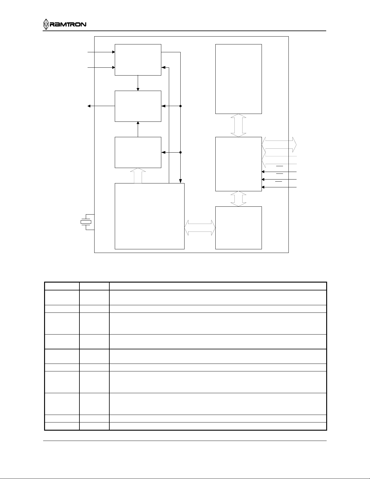
Figure 1. Block Diagram
Pin Description
Pin Name I/O Pin Description
A0-A14 Input Address: The 15 address inputs select one of 32,752 bytes in the FRAM array or one of
16 bytes in the clock/calendar. The address is latched on the falling edge of /CE.
DQ(7:0) I/O Data: Bi-directional 8-bit data bus for accessing the FRAM array and clock.
/CE Input Chip Enable: The active low /CE input selects the device. The falling edge of /CE
internally latches the address. Address changes that occur after /CE has transitioned
low are ignored until the next falling edge occurs.
/OE Input Output Enable: The active low /OE input enables the data output buffers during read
cycles. Deasserting /OE high causes the DQ pins to tri-state.
/WE Input Write Enable: T he active low /WE low enables data on the DQ pins to be written to the
address location latched by the falling edge of /CE.
X1, X2 Input Connect 32.768 kHz crystal.
INT Output Interrupt output: This output can be programmed to respond to the clock alarm, the
watchdog timer, and the power monitor. It is programmable to either active high
(push/pull) or active low (open-drain).
V
Supply Backup Supply Voltage: This supply is used to maintain power for the clock. It must
BAK
remain between 2.5V and V
battery. Current is drawn from V
-0.3V. Typically it is supplied by either a capacitor or a
DD
when VDD is below the V
BAK
voltage.
BAK
VDD Supply Supply Voltage: 5V
VSS Supply Ground.
Rev 0.2
Sept 2001 Page 2 of 27
Page 3
FM3808
y
g
g
Functional Truth Table
/CE /WE /OE Function
H X X Standby/Precharge
!
X X Latch Address
L H L Read
L L X Write
Overview
The FM3808 integrates three complementary but
distinct functions under a common interface in a
single package. First, is the 32Kx8 FRAM memory
block (minus 16 bytes), second is the real-time
clock/calendar, and third is the system supervisor.
The functions are integrated to enhance their
individual performance, so that each provides better
capability than three similar stand-alone devices. All
functions use the same bytewide address/data
interface and are memory mapped. Special functions
including the clock and supervisor are controlled by
registers that reside in the top of the combined
memory map. The register map is described below,
followed by a detailed description of each functional
block.
Register Map
The interface to clock and supervisor functions is via
16 address locations at the top of the address space.
The registers contain timekeeping data, control bits,
or information flags. A short description of each
register follows. Detailed descriptions of each
function follow the register summary.
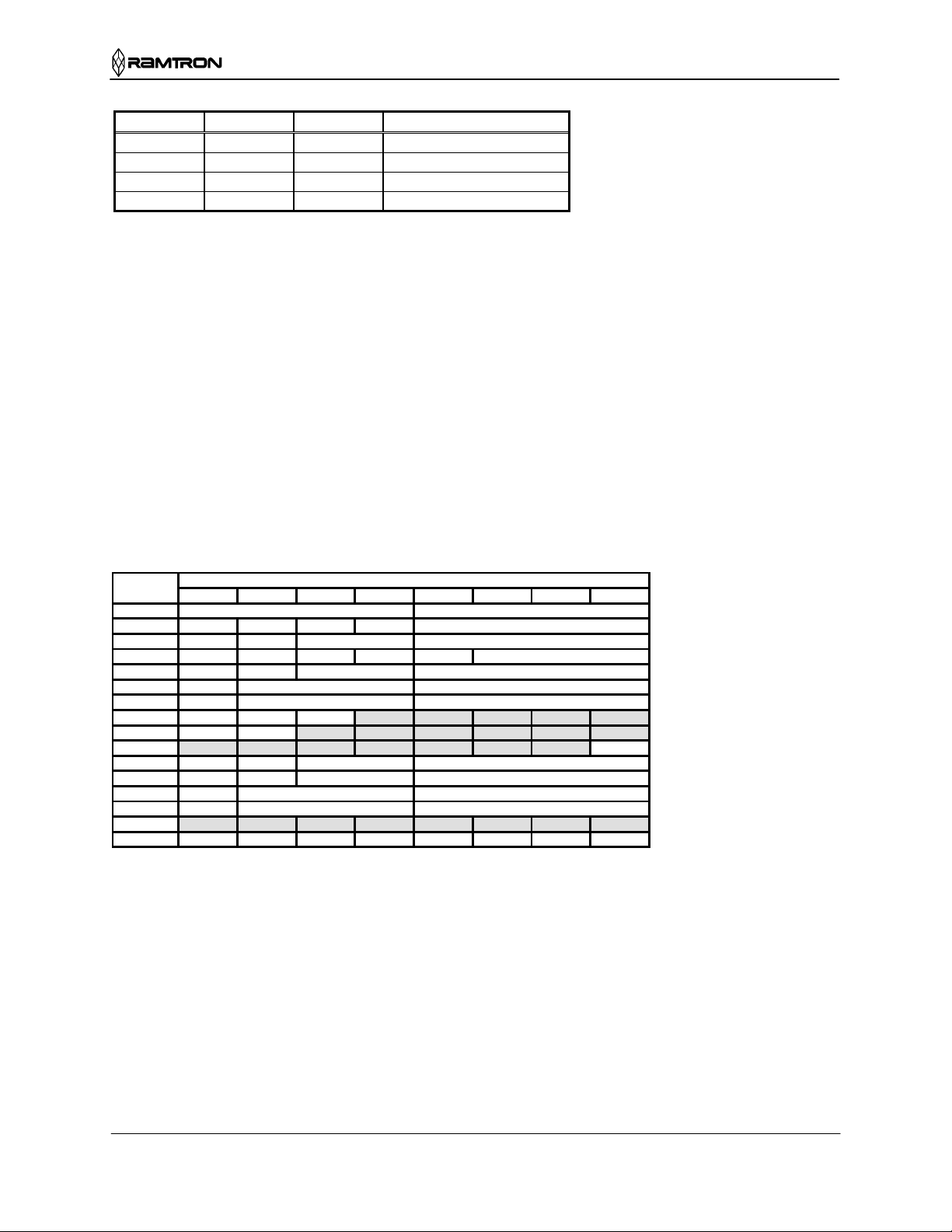
Register Map Summary Table
Address
7FFFh 10 years years
7FFEh
7FFDh
7FFCh
7FFBh
7FFAh
7FF9h
7FF8h
7FF7h
7FF6h
7FF5h
7FF4h
7FF3h
7FF2h
7FF1h
7FF0h
D7 D6 D5 D4 D3 D2 D1 D0 Function Range
00010 mo
00
00000
00
0
0
/OSCEN reserved reserved CALS CAL3 CAL2 CAL1 CAL0 Control-NV
WDS /WDW WDT5 WDT4 WDT3 WDT2 WDT1 WDT0 Watchdo
WIE AIE PFE ABE H/L P/L VINT reserved Interrupts
/Match 0
/Match 0
/Match
/Match
WDF AF PF CF TST CAL W R Fla
Alarm 10 minutes Alarm minutes
Alarm 10 seconds Alarm seconds
10 date date
10 hours hours
10 minutes minutes
10 seconds seconds
Alarm 10 date Alarm date
Alarm 10 hours hours
Data
months
day
Years 00-99
Month 1-12
Date 1-31
Da
Hours 0-23
Minutes 0-59
Seconds 0-59
Alarm Date 1-31
Alarm Hours 0-23
Alarm Minutes 0-59
Alarm Seconds 0-59
User-NV
s/Control
1-7
Note that the shaded bits are implemented in FRAM and therefore are nonvolatile even without backup power.
Rev 0.2
Sept 2001 Page 3 of 27
Page 4
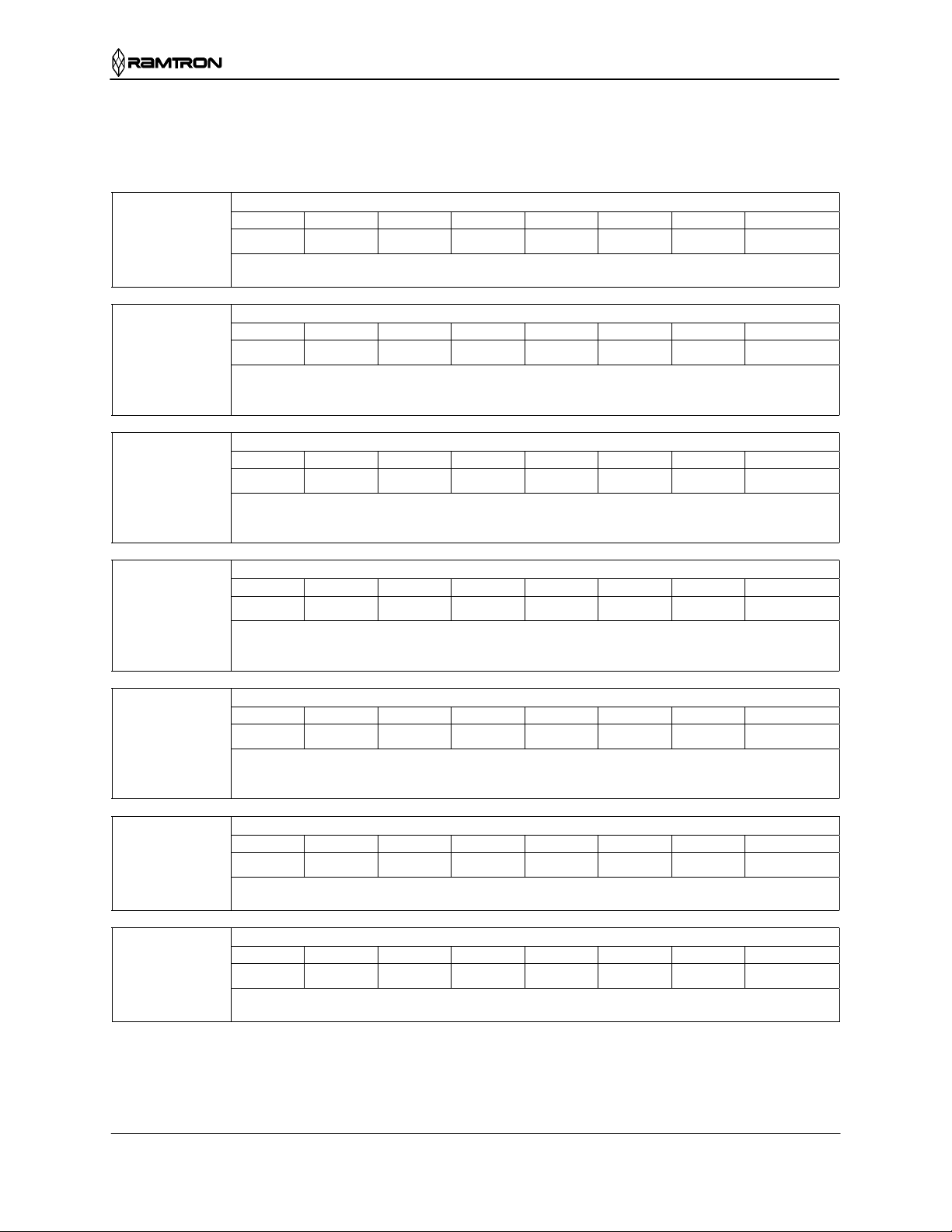
FM3808
Table 1. Register Map
Address Description
7FFFh
Contains the lower two BCD digits of the year. Lower nibble contains the value for years; upper nibble
7FFEh
Contains the BCD digits for the month. Lower nibble contains the lower digit and operates from 0 to 9;
7FFDh
Contains the BCD digits for the date of the month. Lower nibble contains the lower digit and operates
7FFCh
Lower nibble contains a value that correlates to day of the week. Day of the week is a ring counter that
7FFBh
Contains the BCD value of hours in 24-hour format. Lower nibble contains the lower digit and operates
7FFAh
Contains the BCD value of minutes. Lower nibble contains the lower digit and operates from 0 to 9;
7FF9h
Contains the BCD value of seconds. Lower nibble contains the lower digit and operates from 0 to 9;
Timekeeping – Years
D7 D6 D5 D4 D3 D2 D1 D0
10 year.3 10 year.2 10 year.1 10 year.0 Year.3 Year.2 Year.1 Year.0
contains the value for 10s of years. Each nibble operates from 0 to 9. The range for the register is 0-99.
Timekeeping – Months
D7 D6 D5 D4 D3 D2 D1 D0
0 0 0 10 Month Month.3 Month.2 Month.1 Month.0
upper nibble (one bit) contains the upper digit and operates from 0 to 1. The range for the register is 1-
12.
Timekeeping – Date of the month
D7 D6 D5 D4 D3 D2 D1 D0
0 0 10 date.1 10 date.0 Date.3 Date.2 Date.1 Date.0
from 0 to 9; upper nibble contains the upper digit and operates from 0 to 3. The range for the register is
1-31.
Timekeeping – Day of the week
D7 D6 D5 D4 D3 D2 D1 D0
0 0 0 0 0 Day.2 Day.1 Day.0
counts from 1 to 7 then returns to 1. The user must assign meaning to the day value, as the day is not
integrated with the date.
Timekeeping – Hours
D7 D6 D5 D4 D3 D2 D1 D0
0 0 10 hours.1 10 hours.0 Hours.3 Hours2 Hours.1 Hours.0
from 0 to 9; upper nibble (two bits) contains the upper digit and operates from 0 to 2. The range for the
register is 0-23.
Timekeeping – Minutes
D7 D6 D5 D4 D3 D2 D1 D0
0 10 min.2 10 min.1 10 min.0 Min.3 Min.2 Min.1 Min.0
upper nibble contains the upper minutes digit and operates from 0 to 5. The range for the register is 0-59.
Timekeeping – Seconds
D7 D6 D5 D4 D3 D2 D1 D0
0 10 sec.2 10 sec.1 10 sec.0 Seconds.3 Seconds.2 Seconds.1 Seconds.0
upper nibble contains the upper digit and operates from 0 to 5. The range for the register is 0-59.
Rev 0.2
Sept 2001 Page 4 of 27
Page 5
FM3808
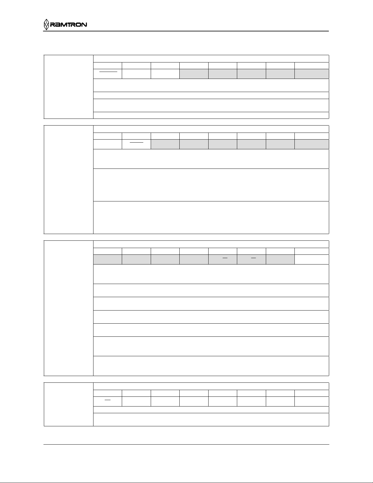
Address Description
7FF8h
/OSCEN /Oscillator Enable. When set to 1, the oscillator is halted. When set to 0, the oscillator runs. Disabling
Reserved Do not use. Should remain set to 0.
CALS Calibration sign. Determines if the calibration adjustment is applied as an addition to or as a subtraction
CAL.3-0 These four bits control the calibration of the clock. These bits are implemented in FRAM.
7FF7h
WDS Watchdog Strobe. Setting this bit to 1 reloads and restarts the watchdog timer. Setting the bit to 0 has no
/WDW Watchdog Write Enable. Setting this bit to 1 masks the watchdog timeout value (WDT.5-0) so it cannot
WDT.5-0 Watchdog Timeout selection. The watchdog timer interval is selected by the 6-bit value in this register.
7FF6h
WIE Watchdog Interrupt Enable. When set to 1 and a watchdog timeout occurs, the watchdog timer drives
AIE Alarm Interrupt Enable. When set to 1, the alarm match drives the interrupt pin as well as the AF flag.
PFE Power-fail Interrupt Enable. When set to 1, the power-fail monitor drives the pin as well as the PF flag.
ABE Alarm Battery-backup Enable. When set to 1, the alarm interrupt (as controlled by AIE) will function
H/L High/Low. When set to a 1, the Interrupt pin is push/pull active high. When set to a 0, the interrupt pin
P/L Pulse/Level. When set to a 1, the interrupt pin is driven active (determined by H/L) by an interrupt
VINT Voltage Interrupt. Selects the voltage on VDD that generates a power-fail flag. When set to a 1, the flag
7FF5h
Contains t he alarm value for the date of the month and the mask bit to select or deselect the date value.
/M
Control-Nonvolatile
D7 D6 D5 D4 D3 D2 D1 D0
OSCEN Reserved Reserved CALS CAL.3 CAL.2 CAL.1 CAL.0
the oscillator can save battery power during storage. On a no battery power up, this bit is set to 1.
from the time-base. This bit is implemented in FRAM. Calibration is explained below
Watchdog Timer
D7 D6 D5 D4 D3 D2 D1 D0
WDS WDW
affect. The bit is cleared automatically once the watchdog timer is reset. The WDS bit is write only.
Reading it always will return a 0.
be written. This allows the user to strobe the watchdog without disturbing the timeout value. Setting this
bit to 0 allows bits 5-0 to be written on the next write to the Watchdog register. The new value will be
loaded on the next internal watchdog clock after the write cycle is complete. This function is explained
in more detail in the watchdog Timer section below.
It represents a multiplier of the 32 Hz count (31.25 ms). The minimum range or timeout value is 31.25
ms (a setting of 1) and the maximum timeout is 2 seconds (setting of 3Fh). Setting the watchdog timer
register to 0 disables the timer. These bits can be written only if the /WDW bit was cleared to 0 on a
previous cycle.
Interrupts
D7 D6 D5 D4 D3 D2 D1 D0
WIE AIE PFE ABE H/L P/L VINT Reserved
the interrupt pin as well as the WDF flag. When set to 0, the watchdog timeout affects only the WDF
flag.
When set to 0, the alarm match only affects the AF flag.
When set to 0, the power-fail monitor affects only the PF flag.
even in battery backup mode. When set to 0, the alarm will occur only when VDD>VLO.
is open drain active low.
source for approximately 200 ms. When set to a 0, the interrupt pin is driven to an active level (as set by
H/L) until the flag register is read.
occurs at 4.75V. When set to 0 the flag occurs at 4.6V. The interrupt pin is enabled by the PFE bit,
otherwise only an internal flag is set.
Alarm – Date of the month
D7 D6 D5 D4 D3 D2 D1 D0
M 0 10 date.1 10 date.0 Date.3 Date.2 Date.1 Date.0
Match. Setting this bit to 0 causes the date value to be used in the alarm match. Setting this bit to 1
causes the match circuit to ignore the date value.
WDT.5 WDT.4 WDT.3 WDT.2 WDT.1 WDT.0
Rev 0.2
Sept 2001 Page 5 of 27
Page 6
FM3808
Address Description
7FF4h
Contains the alarm value for the hours and the mask bit to select or deselect the hours value.
/M Match. Setting this bit to 0 causes the hours value to be used in the alarm match. Setting this bit to 1
7FF3h
Contains t he alarm value for the minutes and th e mask bi t to select or deselect the minutes value
/M Match. Setting this bit to 0 causes the minutes value to be used in the alarm match. Setting this bit to 1
7FF2h
Contains the alarm value for the seconds and the mask bit to select or deselect the minutes value.
/M Match. Setting this bit to 0 causes the seconds value to be used in the alarm match. Setting this bit to1
7FF1h
This register is an uncommitted nonvolatile register. The user register is not manipulated by the real-
7FF0h
WDF Watchdog Timer Flag. This bit is set to 1 when the watchdog timer is allowed to reach 0 without being
AF Alarm Flag. This bit is set to 1 when the time and date match the values stored in the alarm registers
PF Power-fail Flag. This bit is set to 1 when power falls below the power-fail interrupt threshold VINT. It
CF Cen t ury Overflow Flag. This bit is set to a 1 when the values in the years register overflows from 99 to
TST Invokes factory test mode. Users should always set this bit to 0.
CAL Calibration Mode. When set to 1, the clock enters calibration mode. When CAL is set to 0, the clock
W Write Time. Setting the W bit to 1 freezes updates of the timekeeping registers. The user can then write
R Read Time. Setting the R bit to 1 copies a static image of the timekeeping registers and places them in a
Alarm – Hours
D7 D6 D5 D4 D3 D2 D1 D0
M 0 10 hours.1 10 hours.0 Hours.3 Hours2 Hours.1 Hours.0
causes the match circuit to ignore the hours value.
Alarm – Minutes
D7 D6 D5 D4 D3 D2 D1 D0
M 10 min.2
causes the match circuit to ignore the minutes value.
Alarm – Seconds
D7 D6 D5 D4 D3 D2 D1 D0
M 10 sec.2 10 sec.1 10 sec.0 Seconds.3 Seconds.2 Seconds.1 Seconds.0
causes the match circuit to ignore the seconds value.
User-NonVolatile
D7 D6 D5 D4 D3 D2 D1 D0
time clock other than to provide nonvolatile storage of the contents.
Flags/Control
D7 D6 D5 D4 D3 D2 D1 D0
WDF AF PF CF TST CAL W R
reset by the user. It is cleared to 0 when the Flag register is read. It is read-only for the user.
with the match bit(s) = 0. It is cleared when the Flag register is read. It is read -only for the user.
is cleared to 0 when the Fl ag register is read. It is read-only for the user.
00. This indicates a new century, such as going from 1999 to 2000 or 2099 to 2100. The user should
record the new century information as needed. This bit is cleared to 0 when the Flag register is read. It is
read-only for the user.
operates normally.
them with updated values. Setting the W bit to 0 causes the contents of the time registers to be
transferred to the timekeeping counters. This bit affects registers xF, xE, xD, xC, xB, xA, and x9.
holding register. The user can then read them without concerns over changing values causing system
errors. The R bit going from 0 to 1 causes the timekeeping capture, so the bit must be returned to 0 prior
to reading again . This bit affects registers xF, xE, xD, xC, xB, xA, and x9.
10 min.1 10 min.0 Min.3 Min.2 Min.1 Min.0
Rev 0.2
Sept 2001 Page 6 of 27
Page 7

FM3808
Real-time Clock Operation
The real-time clock (RTC) consists of an oscillator, a
divider, and a register system to access the
information. It divides down the 32.768 kHz timebase to provide the user timekeeping resolution of
one second (1Hz). Static registers provide the user
with read/write access to the time values. The
synchronization of these registers with the timekeeper
core is performed using R and W bits in register
7FF0h.
Setting the R bit from 0 to 1 causes a transfer of the
timekeeping information to holding registers that can
be read by the user. If a timekeeper update is in
progress when the R is set, the update will be
completed prior to loading the registers. Another
update cannot be performed unless the R bit is first
cleared to 0 again.
Setting the W bit causes the timekeeper to freeze
updates. Clearing it to 0 causes the values in the time
registers to be written into the timekeeper core. Users
should be sure not to load invalid values, such as FFh
to any of the timekeeping registers.
Updates to the timekeeping core occur continuously
except when frozen. A diagram of the timekeeping
core is shown below.
Backup Power
The real-time clock/calendar is intended for
permanently powered operation. When primary
system power fails, the voltage on V
When it crosses the voltage on the V
will drop.
DD
supply pin,
BAK
the clock power will switch to the backup power
supply V
. The supervisor function, described
BAK
below, controls the switchover process as part of a
more complete power management circ uit.
The clock uses very little current which maximizes
battery life. Although a backup batter y may be used
with the FM3808, the key advantage to combining a
clock function with FRAM is that the configuration
data (shaded regsiter bits in Table 2) is nonvolatile
and does not require a battery backup power source.
Therefore, it is more practical to use a capacitor as a
backup energy source than a battery-backed
RAM/clock combo. With the FM3808, the user has
the choice of using a battery or a capacitor as the
backup source. Some of the parameters used in the
capacitor vs. battery decision include the expected
duration of power outages, the difficulty of resetting
the time if lost, and the cost tradeoff of using a small
battery versus a capacitor.
The following functions are powered from the backup
power source when V
DD
< V
(backup mode) :
BAK
• Clock/calendar core
• Alarm interrupt/comparator
• INT pin driver (determined by ABE & AIE
bits); active low only
• Flags connected to related functions
The following functions are not powered and are
disabled when V
< VLO :
DD
• User interface
• Watchdog timer
• Power monitor & band-gap (V
< ≈ 2.0V)
DD
• Flags connected to related functions
• All FRAM access & updates
• Calibration operation
• INT driver if active high is programmed
Rev 0.2
Sept 2001 Page 7 of 27
Page 8
FM3808
32 Hz
512 Hz
W
32.768 kHz
crystal
CF
Years
8 bits
Months
5 bits
Date
6 bits
Days
3 bits
User Interface Registers
Figure 2. Real-time Clock Core Block Diagram
Calibration
When the CAL bit in register 7FF0.2 is set to 1, the
clock enters calibration mode. Interrupts are disabled
in CAL mode. Calibration operates by applying a
digital correction to the counter based on the
frequency error. In CAL mode, the INT pin is driven
with a 512 Hz nominal square wave. Any measured
deviation from 512 Hz is converted into an error in
ppm. This error corresponds to a correction value that
must then be written by the user into the calibration
register 7FF8h. The correction factors are listed in the
Table 2.
Positive ppm errors require a negative adjustment that
removes pulses. Negative ppm errors require a
positive correction that adds pulses. Positive ppm
adjustments have the CALS bit set to 1, where as
negative ppm adjustments have CALS = 0. After
calibration, the clock will have a maximum error of
Oscillator
Hours
6 bits
Clock
Divider
1 Hz
Minutes
7 bits
Update
Logic
Seconds
7 bits
± 4.34 ppm or ± 0.19 minutes per month at the
calibrated temperature.
The calibration setting is nonvolatile and is stored in
7FF8.4-0. This value only can be written when the
CAL bit is set to a 1. To exit calibration mode, the
user should clear the CAL bit to a 0.
When the calibration mode is entered, the user can
measure the frequency error on the INT pin. This
error expressed in ppm translates directly into
timekeeping error. An offsetting calibration
adjustment corrects this error. However, the
correction is applied by adding or removing pulses on
a periodic basis. Therefore, the correction will not
appear on the 512 Hz output. The calibration
correction must be applied using the values shown in
Table 2. The timekeeping accuracy can be verified by
comparing the FM3808 time to a reference source.
R
Rev 0.2
Sept 2001 Page 8 of 27
Page 9

FM3808
Table 2. Calibration Adjustments
Measured Frequency Range Error Range (ppm)
Min Max Min Max Program Calibration D4-D0
0 512.0000 511.9978 0 4.34 00000b
1 511.9978 511.9933 4.35 13.02 10001b
2 511.9933 511.9889 13.03 21.70 10010b
3 511.9889 511.9844 21.71 30.38 10011b
4 511.9844 511.9800 30.39 39.06 10100b
5 511.9800 511.9756 39.07 47.74 10101b
6 511.9756 511.9711 47.75 56.42 10110b
7 511.9711 511.9667 56.43 65.10 10111b
8 511.9667 511.9622 65.11 73.78 11000b
9 511.9622 511.9578 73.79 82.46 11001b
10 511.9578 511.9533 82.47 91.14 11010b
11 511.9533 511.9489 91.15 99.82 11011b
12 511.9489 511.9444 99.83 108.50 11100b
13 511.9444 511.9400 108.51 117.18 11101b
14 511.9400 511.9356 117.19 125.86 11110b
15 511.9356 511.9311 125.87 134.54 11111b
Measured Frequency Range Error Range (ppm)
Min Max Min Max Program Calibration D4-D0
0 512.0000 512.0022 0 4.34 00000b
1 512.0022 512.0067 4.35 13.02 00001b
2 512.0067 512.0111 13.03 21.70 00010b
3 512.0111 512.0156 21.71 30.38 00011b
4 512.0156 512.0200 30.39 39.06 00100b
5 512.0200 512.0244 39.07 47.74 00101b
6 512.0244 512.0289 47.75 56.42 00110b
7 512.0289 512.0333 56.43 65.10 00111b
8 512.0333 512.0378 65.11 73.78 01000b
9 512.0378 512.0422 73.79 82.46 01001b
10 512.0422 512.0467 82.47 91.14 01010b
11 512.0467 512.0511 91.15 99.82 01011b
12 512.0511 512.0556 99.83 108.50 01100b
13 512.0556 512.0600 108.51 117.18 01101b
14 512.0600 512.0644 117.19 125.86 01110b
15 512.0644 512.0689 125.87 134.54 01111b
Rev 0.2
Sept 2001 Page 9 of 27
Page 10

FM3808
Supervisor Operation
The Supervisor function includes a clock/calendar
alarm, a watchdog timer, and a power monitor. A
programmable interrupt pin provides maximum
functionality to permit the host processor to benefit
from the supervisor functions. It is designed to allow
either reset or interrupt capability to the external
processor ho st.
Alarm
The alarm function compares user-programmed
values to the corresponding time of day values. When
a match occurs, the alarm event occurs. The alarm
offers an internal flag bit and an optional external
interrupt.
There are four alarm match values. They are date of
the month, hours, minutes, and seconds. The match
select bits determine if a value is used in the alarm
match selection. Setting the match select bit to ‘0’
indicates that the corresponding value should be used
in the match process.
Depending on the match select bits, the alarm can
occur as specifically as one particular second on one
day of the month, or as frequently as once per second
continuously. Each match select bit is contained in
the MSB of the match value register. The match
select bits work in concert as shown in the table
below. Selecting none of the match bits (all ‘1’s)
indicates that no match is required. The alarm occurs
every second. Setting the match select bit for seconds
to ‘0’ causes the logic to match the seconds alarm
value to the current time of day. Since a match will
occur for only one value per minute, the alarm occurs
once per minute. Likewise setting the seconds and
minutes match select bits causes an exact match of
these values. Thus, an alarm will occur once per hour.
Setting seconds, minutes, and hours causes a match
once per day. Lastly, selecting all match-values
causes an exact time and date match. Selecting other
bit combinations will not produce meaningful results,
however the alarm circuit should follow the functions
described.
The alarm event can be detected by the user in two
ways. First, the AF flag bit in the register 7FF0.6 will
indicate that a match has occurred. The AF bit will be
set to 1 when a valid match occurs. Reading the flag
register clears the alarm flag bit (and all others).
Second, a hardware interrupt pin will be provided.
The interrupt function is described below.
Alarm Match Bits
Seconds Minutes Hours Date Alarm condition
1 1 1 1 No match required = alarm 1/second
0 1 1 1 Alarm when seconds match, = alarm 1/minute
0 0 1 1 Alarm when seconds, minutes match, = alarm 1/hour
0 0 0 1 Alarm when seconds, minutes, hours match, = alarm 1/day
0 0 0 0 Alarm when seconds, minutes, hours, date match, = alarm 1/month
Rev 0.2
Sept 2001 Page 10 of 27
Page 11

FM3808
Watchdog Timer
The Watchd og timer is a free running down counter
that uses the 32 Hz clock (31.25 ms) derived from the
crystal oscillator. The oscillator must be running
(/OSCEN=0) for the watchdog to function. It begins
counting down from the value loaded in the
Watchdog timer register (7FF7h).
The counter consists of a loadable register and a free
running counter. On power up, the watchd og timeout
value in 7FF7h is loaded into the counter load
register. Counting begins on power up and restarts
from the loadable value any time the Watchdog
Strobe (WDS – 7FF7.7) WDS bit is set to 1. The
counter is compared to terminal value of 0. If the
counter reaches this value, it causes an internal flag
and an optional interrupt output (see interrupts
below). The user can prevent the timeout interrupt by
setting WDS bit to 1 prior to the counter reaching 0.
This causes the counter to be reloaded with the
watchdog timeout value and to be restarted. As long
as the user sets the WDS bit prior to the counter
reaching the terminal value, the interrupt and flag
never occurs.
New timeout values can be written by setting the
watchdog write bit (/WDW – 7FF7.6) to 0. When the
/WDW bit is 0 (from a previous operation), new
writes to the watchdog timeout value 7FF7.5-0 allow
the timeout value to be modified. When /WDW is a 1,
then writes to bits 7FF7.4-0 will be ignored. The
/WDW function allows a user to set the WDS bit
without concern that the watchdog timer value will be
modified. A logical diagram of the watchdog timer is
shown below. Note that setting the watchdog timeout
value to 0 would be otherwise meaningless and
therefore disables the watchdog function.
The output of the watchdog timer is a flag bit (WDF
– 7FF0.7) that is set if the watchdog is allowed to
timeout. The flag is set upon a watchdog timeout and
cleared when the flag register is read by the user. The
user can also enable an optional interrupt source to
drive the interrupt pin if the watchdog timeout occurs.
The interrupt function is described below.
Oscillator
32.768 kHz
Clock
Divider
1 Hz
32 Hz
7FF0.7
WDF
WDS
WDW
Counter
Zero
Compare
Load Register
QD
Q
7FF7.5-0
Watchdog
write to
register
Watchdog
register
Figure 3. Watchdog Timer Block Diagram
Rev 0.2
Sept 2001 Page 11 of 27
Page 12

FM3808
Power Monitor
The FM3808 provides a power management scheme
with either power-fail interrupt or processor-reset
capability. It also controls the internal switch to
backup power for the timekeeper and protects the
memor y from l ow-V
access. The power monitor is
DD
based on an internal band-gap reference circuit that
compares the incoming V
to various thresholds.
DD
The power monitor compares V
The first is an interrupt threshold (V
to three thresholds.
DD
), which can be
INT
selected between two levels as shown below. When
V
drops below the programmed V
DD
level, the
INT
event will set the power fail flag (PF – 7FF0.5). It
also can drive the interrupt pin as described in the
interrupt section below. The interrupt level selection
is controlled via the voltage interrupt bit (V
INT
–
7FF6.1) as follows.
Power fail V
INT
4.6V 0
4.75V 1
If the power monitor is used to reset the external
processor, then the lower threshold is more likely to
be used. If the power monitor is providing an early
warning interrupt, then either may be suitable
depending on expected slew rates and the amount of
data to be saved on power failure.
below V
begin to draw power from V
event may be above or below the V
depending on whether a battery or capacitor backup is
used.
To conserve the life of the backup source, the power
monitor circuit is only operated from V
has dropped too low for the monitor to work, it ceases
operation. However, the power monitor will
reenergize as V
after the band-gap energizes, the reverse sequence
will occur. As soon as the band gap is functional, it
will re-assert both selections for switch over and
power fail. As the V
will be removed, allowing memory access and
operating the clock from V
V
, the power-fail condition will be removed. Note
INT
that the PF flag will not be cleared until the flag
register is read.
The following figure illustrates the various events
tracked by the power monitor.
VDD
VINT VINT
VLO VLO
VBAK
. When switchover occurs, the clock will
BAK
rather than VDD. This
BAK
or VLO level
INT
. When VDD
DD
rises on power-up. On power-up,
DD
rises further, the switchover
DD
. As the VDD rises above
DD
BG BG
VBAK
The second threshold is the low V
This level, which is called V
writes to the FRAM array, which may result in lost
data. At this time, access to the memory array and
clock registers will be blocked until V
V
. VLO is always below V
LO
V
, inputs will be ignored. On power up, the chip
LO
enable input will be ignored while V
but must be inactive (high) when V
level.
The third threshold is the switch of the internal supply
from V
to V
DD
for the timekeeper. This
BAK
switchover will occur at the level when V
memor y lock out.
DD
, prevents low voltage
LO
rises above
DD
. When VDD is below
INT
is below VLO,
DD
reaches the VLO
DD
crosses
DD
Figure 4. Power Monitor Events
In the diagram, BG is the voltage at which the bandgap will function. This voltage is not precisely
specified but is well below the range of operation for
the memory or other circuits. On power down, the
band-gap will monitor V
allows a brownout to occur where V
as long as possible. This
DD
returns to a
DD
proper level prior to the band-gap failing. Since the
band-gap runs only from V
, it does not reduce the
DD
life of the backup source.
Rev 0.2
Sept 2001 Page 12 of 27
Page 13

FM3808
Interrupts
The supervisor was designed to serve diverse
applications. Its sophistication is managed by the
interrupt block, which makes this functionality
available to the host system. The interrupt block is
capable of providing interrupt or reset conditions, and
even can power up a system at a preprogrammed
time. The function is described as an interrupt, even
though the output may be used as a reset source.
The supervisor provides three potential interrupt
sources. They include the watchdog timer, the power
monitor, and the clock/calendar alarm. Each can be
individually enabled and assigned to drive the single
INT pin. In addition, each has a flag bit associated
with it so that the host processor can determine the
cause of the interrupt.
Some of the sources have additional control bits that
determine functional behavior. In addition, the pin
interrupt occurs. A functional diagram of the interrupt
logic is shown below.
As shown, the three interrupts each have a source and
an enable. Both the source and the enable must be
active (true high) in order to generate an interrupt
output. Only one source is necessary to drive the pin.
The user can identify the source by reading the flag
register, which contains the flags associated with each
source. All flags are cleared to 0 when the register is
read. The cycle must be a complete read cycle,
otherwise the flags will not be cleared if the /WE
signal goes low. The power monitor has two
programmable settings that are explained above in the
power monitor section.
Once an interrupt source is active, the pin driver
determines the behavior of the output pad. It has two
programmable settings as shown below. Pin driver
control bits are located in the Interrupts register
7FF6h.3-2.
driver has three bits that specify its behavior when an
WDF
Watchdog
Timer
WIE
VDD
P/L
PF
Power
Monitor
PFE
Pin
Driver
INT
VINT
H/L
ABE
AF
Clock
Alarm
AIE
Figure 5. Interrupt Block Diagram
According to the programming selections, the pin can
be driven in the backup mode for an alarm interrupt
or not. In addition, the pin can be active low (opendrain) or active high (push-pull) driver. If
programmed for operation during backup mode, it
can only be active low. Lastly, the pin can provide a
one-shot function so that the active condition is a
pulse, or a level operation. In one-shot mode, the
pulse width is fixed at approximately 200 ms. This
mode is intended to reset a host microcontroller. In
level mode, the pin goes to its active polarity until the
Rev 0.2
Sept 2001 Page 13 of 27
Flag register is read by the user. This mode is
intended to be used as an interrupt to a host
microcontroller. The control bits are summarized as
follows.
Watchdog Interrupt Enable
- WIE. When set to 1, the
watchdog timer drives the interrupt pin as well as an
internal flag when a watchdog timeout occurs. When
set to 0, the watchdog timer affects only the internal
flag.
Page 14

FM3808
Alarm Interrupt Enable – AIE. When set to 1, the
alarm match drives the interrupt pin as well as an
internal flag. When set to 0, the alarm match only
affects the internal flag.
Power-fail Interrupt Enable
- PFE. When set to 1, the
power-fail monitor drives the pin as well as an
internal flag. When set to 0, the power-fail monitor
affects only the internal flag.
Alarm Battery-backup Enable
- ABE. When set to 1,
the clock alarm interrupt (as controlled by AIE) will
function even in battery backup mode. When set to 0,
the alarm will occur only when V
> VLO. AIE
DD
should only be set when the interrupt pin is
programmed for active low operation. In addition, it
only functions with the clock alarm, not the
watchdog. If enabled, the power monitor will drive
the interrupt during all normal V
conditions
DD
regardless of the ABE bit. The application for ABE is
intended for power control, where a system powers
up at a predetermined time. Depending on the
application, it may require dedicating the INT pin to
this function.
High/Low
– H/L. When set to a 1, the INT pin is
active high ( push-pull). The INT pin can drive high
only when V
DD>VLO
. When set to a 0, the interrupt
pin is active low (open-drain). It can function as a
pull down even in battery backup mode.
Pulse/Level
– P/L. When set to a 1, the INT pin is
driven (by an interrupt source) for approximately 200
ms. When P/L is set to a 0, the interrupt pin is driven
high or low (as set by H/L) until the flag register is
read.
When an enabled interrupt source activates the INT
pin, an external host can read the flag register to
determine the cause. One or more flags may be set
when the register is read, however all will be cleared
when the register is read. If the INT pin is
programmed for level mode, then the condition will
clear and the INT pin will return to its inactive state.
If the pin is programmed for pulsed operation, then
reading the flag also will clear the flag and the pin.
The pulse will not complete its specified duration if
the flag register is read. Of course, if the INT pin is
used to reset the host, then the flag register would not
be read during an active pulse. Care should be taken
in reading the flags as a new source may occur after
the pin goes active but before the register is read.
During a power-on reset with no battery, the interrupt
register is automatically loaded with the value 24h.
This causes power fail interrupt to be enabled with an
active low pulse.
Rev 0.2
Sept 2001 Page 14 of 27
Page 15

FM3808
FRAM Memory Operation
The memory array is logically organized as 32,768 x
8 with the upper 16 bytes disabled and allocated to
the RTC. It is accessed using an industry standard
SRAM-type parallel interface. It is virtually identical
to the 32Kx8 FM1808 in function. The memory array
in the FM3808 is inherently nonvolatile via its unique
ferroelectric process. All data written to the part is
immediately nonvolatile with no delay. Functional
operation of the FRAM memory is similar to SRAM
type devices. The major operating difference between
the FRAM array and an SRAM (besides nonvolatile
storage) is that the FM3808 latches the address on the
falling edge o f / C E.
Users access 32,752 memory locations each with 8
data bits through a parallel interface. The complete
15-bit address specifies each of 32,768 bytes
uniquely, with the upper 16 locations allocated to
timekeeping functions. Internally, the memory array
is organized into 32 blocks of 8Kb each. The 5 mostsignificant address lines decode one of 32 blocks.
This blo ck segmentation has no effect on o peration,
however the user may wish to group data into blocks
by its endurance requirements as explained in a later
section.
The access and cycle time are the same for read and
write memory operations. Writes occur immediately
at the end of the access with no delay. A precharge
operation, where /CE goes inactive, is a part of every
memory cycle. Thus unlike SRAM, the access and
cycle times are not equal.
The FM3808 is designed to operate in a manner very
similar to other bytewide memory products. For users
familiar with BBSRAM, the performance is
comparable but the bytewide interface operates in a
slightly different manner as described below. For
users familiar with EEPROM, the obvious differences
result from the higher write-performance of FRAM
technology including NoDelay writes and much
higher write-endur ance.
Read Operation
A read o peration begins on the fal ling edge of /CE.
At this time, the address bits are latched and a
memory cycle is initiated. Once started, a full
memory cycle will be completed internally even if the
/CE is taken inactive. Data becomes available on the
bus after the access time has been satisfied.
After the address has been latched, the address value
may be changed upon satisfying the hold time
parameter. Unlike an SRAM, changing address values
will have no effect on the memory operation after the
The FM3808 will drive the data bus when /OE is
asserted low. If /OE is asserted after the memory
access time has been satisfied, the data bus will be
driven with valid data. If /OE is asserted prior to
completion of the memory access, the data bus will
not be driven until valid data is available. This feature
minimizes supply current in the system by eliminating
transients due to invalid data. When /OE is inactive,
the data bus will remain tri-stated.
Write Operation
Writes occur in the FM3808 in the same time interval
as reads. The FM3808 supports both /CE and /WE
controlled write cycles. In all cases, the address is
latched on the falling edge of /CE.
In a /CE controlled write, the /WE signal is asserted
prior to beginning the memory cycle. That is, /WE is
low when /CE falls. In this case, the part begins the
memory cycle as a write. The FM3808 will not drive
the data bus regardless of the state of /OE.
In a /WE controlled write, the memory cycle begins
on the falling edge of /CE. The /WE signal falls after
the falling edge of /CE. Therefore, the memory cycle
begins as a read. The data bus will be driven
according to the state of /OE until /WE falls. The
timing of both /CE and /WE controlled write cycles is
shown in the electrical specifications.
Write access to the array begins asynchronously after
the memory cycle is initiated. The write access
terminates on the rising edge of /WE or /CE,
whichever is first. Data set-up time, as shown in the
electrical specifications, indicates the interval during
which data cannot change prior to the end of the write
access.
Unlike other truly nonvolatile memory technologies,
there is no write delay with FRAM. Since the read
and write access times of the underlying memory are
the same, the user experiences no delay through the
bus. The entire memory operation occurs in a single
bus cycle. Therefore, any operation including read or
write can occur immediately following a write. Data
polling, a technique used with EEPROMs to
determine if a write is complete, is unnecessary.
Precharge Operation
The precharge operation is an internal condition
where the state of the memory is prepared for a new
access. All memory cycles consist of a memory
access and a precharge. The precharge is user
initiated by taking the /CE signal high or inactive. It
must remain high for at least the minimum precharge
timing specification. The user dictates the beginning
address is latched.
Rev 0.2
Sept 2001 Page 15 of 27
Page 16

FM3808
FFFFh
of this operation since a precharge will not begin until
/CE rises. Ho wever, the de vice has a maximum /CE
low time specification that must be satisfied.
Memory Architecture
FRAM memory internally operates with a read and
restore mechanism similar to a DRAM. Therefore
each cycle (read or write) involves a change of state.
The memory architecture is based on an array of rows
and columns. Each access causes an endurance cycle
Block 31
Block 31
Block 30
Block 30
Block 29
Block 29
Block 28
Block 28
FFFFh
FC00h
FC00h
FBFFh
FBFFh
F800h
F800h
F7FFh
F7FFh
F400h
F400h
F3FFh
F3FFh
F000h
F000h
for an entire row (4 bytes). The memory array is
divided into 32 blocks, each 1Kx8. The 5-upper
address lines decode the block selection as shown in
Figure 6. Data targeted for significantly different
numbers of cycles should be located in separate
blocks since memory rows do not extend across block
boundaries.
Each block of 1Kx8 consists of 256 rows and 4
column address locations. The address lines A0-A7
decode row selection and A8-A9 lines decode column
selection. This scheme facilitates a relatively uniform
distribution of cycles across the rows of a block. By
Block 3
Block 3
Block 2
Block 2
Block 1
Block 1
Block 0
Block 0
0FFFh
0FFFh
0C00h
0C00h
0BFFh
0BFFh
0800h
0800h
07FFh
07FFh
0400h
0400h
03FFh
03FFh
0000h
0000h
allowing the address LSBs to decode row selection,
the user avoids applying multiple cycles to the same
row when accessing sequential data. For example,
256 bytes can be accessed sequentially without
accessing the same row twice. In this example, one
cycle would be applied to each row. An entire block
of 1Kx8 can be read or written with only four cycles
applied to each row. Figure 7 illustrates the
Figure 6. Address Blocks
A
9-A8
11b
Block 4
A14-A10
00100b
organization within a memory block.
10b
Row 0
Row 1
Row 2
01b
Row 3
Row 252
Row 253
Row 254
Row 255
00b
02h 03h
00h FFh
A0-A7
Figure 7. Row and Column Organization
01h
FCh
FDh
FEh
Rev 0.2
Sept 2001 Page 16 of 27
Page 17

FM3808
FRAM Design Considerations
When designing with FRAM for the first time, users
of SRAM will recognize a few minor differences.
First, bytewide FRAM memories latch each address
on the falling edge of chip enable. This allows the
address bus to change after starting the memory
access. Since every access latches the memory
address on the falling edge of /CE, users should not
ground it as they might with SRAM.
Users that are modifying existing designs to use
FRAM should examine the hardware address
decoders. Decoders should be modified to qualify
addresses with an address valid signal if they do not
already. In many cases, this is the only change
required. Systems that drive chip enable active, then
inactive for each valid address may need no
modifications. An example of the target signal
relationships are shown in Figure 8. Also shown is a
common SRAM signal relationship that will not
work
for the FM3808.
Valid Memory Signaling Relationship
FRAM
signaling
CE
Address
Data
Address 1 Address 2
Data 1 Data 2
Invalid Memory Signaling Relationship
SRAM
signaling
CE
Address
Data
Address 1
Data 1
Figure 8. Memory Address Relationships
Address 2
Data 2
Rev 0.2
Sept 2001 Page 17 of 27
Page 18

FM3808
Real-time Clock Design Considerations
The principal design issues in using the real time
clock are selection and specification of backup
energy source and the selection of the timekeeping
crystal. Selection of the backup source is primarily a
choice between a capacitor and a battery, and the
specifications needed for each. Selection of the
crystal is based on mechanical (surface mount versus
through-hole) considerations and the characteristic
capacitance. Each topic is discussed briefly.
Backup Power Source
The FM3808 is designed to accommodate either a
battery or a capacitor as a backup power source.
Unlike SRAM-based timekeepers that depend on the
battery to make data nonvolatile, the FM3808 is
unrestricted. Data stored in FRAM is not dependent
on the backup battery in any way. This means that
capacitor backup, which should be less expensive, is
a option. Selection of a capacitor is determined by the
expected duration of power outage where
timekeeping must be maintained, and the practical
difficulty in resetting the time should it be lost. If the
time is relatively easy to reset, or a typical power loss
is only a brownout, the capacitor may be a good, cost
effective choice. In addition, portable systems that
use a battery for primary power are good candidates
for capacitor backup. If the time is very difficult to
reset, or the power outage may be longer than a
capacitor can supply, then a small battery is best.
Each system and application can be evaluated for the
difficulty in setting the time. However, the expected
backup times for several capacitor choices are
illustrated below. These figures cannot be used as
guarantees due to the unknown leakage characteristic s
in external components, but they provide guidelines
for realistic expectations about capacitor use. In the
5V Supply
scenario using capacitor backup, the charging circuit
must also be considered. A typical representation is
shown below.
The backup times are based on a starting backup
voltage (fully char ged) of 4 .7V and minimum backup
voltage of 2.5V. A 0.3V forward drop from 5.0V
VDD might be expected from a schottky-diode. Note
the graph, which shows approximate backup current
as a function of backup voltage. Thus, the higher
voltages at the beginning of discharge provide less
incremental backup time than the lower voltages near
the end of discharge. However, the total backup time
depends on the capacitor size and the maximum, fully
charged volt age.
One important note about capacitor backup is that the
times are incremental. Each time power is restored
the capacitor is fully recharged. Rather than
examining the cumulative time without power in the
system over a 10-year period, the capacitor design is
only concerned with the maximum time without
power for one outage.
If the times available for a capacitor are not
sufficient, then a battery is the best selection. Most
users opt for a 3V lithium coin. Note that with nonrechargeable batteries, the reservoir is not replenished
so the critical parameter is the total time without
power during the useful life of a system. For 1 year
without power (total) during a 10-year system life, the
battery capacity must be at least 9.25 mAhr. For 5
years without power during a 10-year period, it
becomes 46 mA*hr.
x
1
VDD
Schottky
Diode
Capacitor Size Backup Time
x
2
FM3808
VBAK
Backup Capacitor or
Super/Golden Cap
100 µF 3 minutes
1000 µF 30 minutes
10000 µF 5.1 hours
0.47 F (super cap) 240 hours
Figure 9. Capacitor Backup Circuit
Rev 0.2
Sept 2001 Page 18 of 27
Page 19

FM3808
IBAK vs VBAK
2.5E-06
2.0E-06
1.5E-06
IBAK
1.0E-06
5.0E-07
0.0E+00
4.7 4.5 4.25 4 3.75 3.5 3.25 3 2.75 2.5
VBAK
Figure 10. Backup Current vs. Voltage
Crystal Selection
The second passive component needed for the RTC
function is the timekeeping crystal. A 32.768 kHz
time-base is required, and the FM3808 is designed to
accept a low cost crystal. The major parameters
associated with the crystal are timekeeping accuracy
and backup current. The FM3808 is designed to
accept a crystal with a characteristic capacitance of 6
pF. Deviations from this specification will lead to
different accuracy and IBAK from the specified
IBAK may go up or down from the specified value as
a function of the capacitive load.
The timekeeping accuracy is also a strong function of
the operating temperature due to errors in crystal
frequency. Temperature behavior of timekeeping
crystals is well known and it follows a curve like the
one shown below. The specific crystal manufacturer
should be consulted for the behavior of their specific
device. Note the error in frequency ppm. One ppm is
roughly 2.6 seconds per month in timekeeping error.
values. Though accuracy is unlikely to improve, the
0
-20
-40
-60
-80
-100
Error ppm
-120
-140
-160
-180
-200
-45
-35
-25
-15
5
-5
Ambient Temperature
15
C
25
35
45
55
65
75
85
Figure 11. Typical Crystal Error vs. Temperature
Rev 0.2
Sept 2001 Page 19 of 27
Page 20

FM3808
Electrical Specifications
Absolute Maximum Rat ing s
Symbol Description Ratings
VDD Power Supply Voltage with respect to VSS -1.0V to +7.0V
VIN Voltage on any signal pin with respect to VSS -1.0V to +7.0V and
V
< VDD+1.0V
IN
T
Storage temperature
STG
T
Lead temperature (Soldering, 10 seconds)
LEAD
Stresses above those listed under Absolute Maximum Ratings may cause permanent damage to the device.
This is a stress rating only, and the functional operation of the device at these or any other conditions above
those listed in the operational section of this specification is not implied. Exposure to absolute maximum
ratings conditions for extended periods may affect device reliability.
DC Operating Conditions (T
= -40° C to + 85° C, VDD = 4.5V to 5.5V unless otherwise specified)
A
Symbol Parameter Min Typ Max Units Notes
VDD Power Supply Voltage 4.5 5.0 5.5 V
V
VDD Voltage that activates INT pin 4.6
INT
4.45
V
Clock Backup Voltage 2.5 3.0 VDD V
BAK
VLO VDD Lockout Voltage 4.3 4.5 V 11
VSW VDD Voltage that causes switch to V
V
BAK
VBG VDD Voltage for active Power Monitor 2.3 V 5
IDD V
I
Standby Current - TTL 500
SB1
I
Standby Current - CMOS 150
SB2
I
Clock backup current 0.9 1.0
BAK
Supply Current - Active 10 25 mA 1
DD
ILI Input Leakage Current 10
ILO Output Leakage Current 10
VIH Input High Voltage 2.0 VDD + 0.5 V
VIL Input Low Voltage -0.5 0.8 V
VOH Output High Voltage 2.4 V 10
VOL Output Low Voltage 0.4 V 9
V
Output Low Voltage (INT pin)
OLB
Device in backup mode (V
DD<VBAK
)
0.7 V 12
Notes
VDD = 5.5V, /CE cycling at minimum cycle time. All inputs at CMOS levels, all outputs unloaded.
1.
2.
Voltage for V
3.
V
= 3.0V, VDD < V
BAK
4.
VSW occurs when VDD drops below V
rather than from V
5.
Signals controlled by the power monitor (such as the INT output) are active.
6.
VDD = 5.5V, /CE at VIH, All inputs at TTL levels, all outputs u nloaded .
7.
VDD = 5.5V, /CE at VIH, All inputs at CMOS levels, all outputs unloaded.
8.
VIN, V
9.
10.
11.
12.
OUT
IOL = 4.2 mA.
IOH = -2.0 mA.
Memory and register access is blocked when VDD < VLO
VDD=0, V
depends on selection of V
INT
between VDD and VSS.
= 3.0V, IOL = 4.2 mA
BAK
; oscillator running.
BAK
. VSW is not otherwise used for control signals or functions.
DD
control bit.
INT
. VSW is also the point at which the timekeeper draws current from the V
BAK
-40°C to + 85°C
300° C
4.75
4.6
V 4
BAK
V
V
µA
µA
µA
µA
µA
BAK
2
6
7
3
8
8
pin,
Rev 0.2
Sept 2001 Page 20 of 27
Page 21

FM3808
Read Cycle AC Parameters (T
= -40° C to + 85° C, VDD = 4.5V to 5.5V unless otherwise specified)
A
Symbol Parameter Min Max Units Notes
tCE Chip Enable Access Time ( to data valid) 70 ns
tCA Chip Enable Active Time 70 10,000 ns
tRC Read Cycle Time 130 ns
tPC Precharge Time 60 ns
tAS Address Setup Time 0 ns
tAH Address Hold Time 10 ns
tOE Output Enable Access Time 10 ns
tHZ Chip Enable to Output High-Z 15 ns 1
t
Output Enable to Output High-Z 15 ns 1
OHZ
Write Cycle AC Parameters (T
= -40° C to + 85° C, VDD = 4.5V to 5.5V unless otherwise specified)
A
Symbol Parameter Min Max Units Notes
tCA Chip Enable Active Time 70 10,000 ns
tCW Chip Enable to Write High 70 ns
tWC Write Cycle Time 130 ns
tPC Precharge Time 60 ns
tAS Address Setup Time 0 ns
tAH Address Hold Time 10 ns
tWP Write Enable Pulse Width 30 ns
tDS Data Setup 30 ns
tDH Data Hold 0 ns
tWZ Write Enable Low to Output High Z 15 ns 1
tWX Write Enable High to Output Driven 10 ns 1
tHZ Chip Enable to Output High-Z 15 ns 1
tWS Write Setup 0 ns 2
tWH Write Hold 0 ns 2
Notes
1 This parameter is periodically sampled and not 100% tested.
2 The relationship between /CE and /WE determines if a /CE- or /WE-controlled write occurs. There is no timing
specification associated with this relationship.
Power Cycle Timing (T
= -40° C to + 85° C)
A
Symbol Parameter Min Max Units Notes
t
INT signal active after V
INT
100 ns 1,2
INT
tPD Last Access Complete to VLO 0 ns 1,3
tRI VLO to inputs recognized on power-up 1
tR Rise time of VDD from VBG to VLO 100
tF Fall time of VDD from VLO to VBG 100
µs
µs
µs
1,4
1,5
1,5
Notes
1 This parameter is periodically sampled and not 100% tested.
2 If power monitor is programmed to generate INT.
3 Access is blocked at V
may be useful in accomplishing th is.
4 Failing to satisfy tRI may result in the first access b eing ign ored. Failure to raise /CE to a h igh level p rior to VDD>VLO may
result in improper operation.
5 Slew rate for proper transition between the locked-out condition and normal operation.
. The last access should be complete prior to reaching VLO. The early warning power fail interrupt
LO
Rev 0.2
Sept 2001 Page 21 of 27
Page 22

FM3808
Supervisor AC Parameters (T
= -40° C to + 85° C, VDD = 4.5V to 5.5V unless otherwise specified)
A
Symbol Parameter Min Typ Max Units Notes
t
INT output pulse width 150 200 300 ms 1
IPU
t
Flag register access to INT pin clear - 100 ns 2
FCO
Notes
1 P/L = 1; pulse mode.
2 P/L= 0; level mode. From the end of the access where th e flag regi st er is read and the flag cleared.
Data Retention (
VDD = 4.5V to 5.5V unless otherwise specified)
Parameter Min Units Notes
Data Retention 10 Years 1
Notes
1. The relationship between retention, temperature, and the associated reliability
level will be characterized separately.
Capacitance
(TA = 25° C, f=1.0 MHz, VDD = 5V)
Symbol Parameter Max Units Notes
CIO Input/output capacitance (DQ) 8 pF 1
CI Input capacitance 6 pF 1
C
X1, X2 Crystal pin capacitance 12 pF 1, 2
XTAL
Notes
1 This parameter is periodically sampled and not 100% tested.
2 The crystal attached to the X1/X2 pins must be rated as 6pF max.
AC Test Conditions Equivalent AC Load Circuit
Input Pulse Levels 0 to 3V
Input rise and fall times 10 ns
1.3V
Input and output timing levels 1.5V
3300
Ω
Output
50 pF
Rev 0.2
Sept 2001 Page 22 of 27
Page 23

FM3808
Timing Diagrams
CE
t
t
AH
AS
A0-14
t
OE
OE
DQ0-7
t
RC
t
CA
t
PC
t
OHZ
t
CE
t
HZ
Read Cycle Timing
t
WC
t
CA
t
PC
CE
t
t
AH
AS
A0-14
t
WS
t
WH
WE
OE
DQ0-7
t
DS
t
DH
Write Cycle Timing - /CE Controlled Timing
Rev 0.2
Sept 2001 Page 23 of 27
Page 24

FM3808
t
WC
t
CA
t
PC
CE
t
t
AH
AS
A0-14
t
WH
WE
t
WS
t
WP
OE
t
WZ
t
WX
DQ0-7
out
t
t
DS
DH
DQ0-7
in
Write Cycle Timing - /WE Controlled Timing
Rev 0.2
Sept 2001 Page 24 of 27
Page 25

FM3808
Picture assumes VSW < VINT
VDD
t
F
VINT
VLO VLO
VSW
VBG
t
INT
t
R
VINT
VSW
VBG
t
FCO
t
IPU
INT
t
PD
t
RI
Inputs
CE
Power Cycle Timing
INT
source
occurs
INT
source
occurs
P/L=1 P/L=0
t
IPU
INT
t
FCO
CE
INT source
flag cleared
INT Pin Timing
Rev 0.2
Sept 2001 Page 25 of 27
Page 26

FM3808
Mechanical Drawing
32-pin TSOP (JEDEC MO-142 BA)
All dimensions in millimeters
13.30-13.55
11.70-11.90
1
2
3
7.90-8.10
1.20
max
0.50
typ
0.17-0.27
typ
0.95-1.05
0.05-0.15
13.30-13.55
R 0.08 min
R 0.08-0.20
°°
0.50-0.70
0 - 5
Rev 0.2
Sept 2001 Page 26 of 27
Page 27

FM3808
Revision History
Revision Date Summary of Changes
0.1 Dec 19, 2000 Initial Release
0.2 Sept 19, 2001 Changed ISB spec, redefined crystal capacitance specs, data retention
temperature condition. General cleanup.
Rev 0.2
Sept 2001 Page 27 of 27
 Loading...