

Page 1
Preliminary
NCN
N
NCN
FM3135
Integrated RTC/Alarm/F-RAM & Embedded Crystal
Features
High Integration Device Replaces Multiple Parts
• Serial Nonvolatile Memory
• Real-time Clock (RTC) with Alarm
• Clock Output (Programmable frequency)
64Kb Ferroelectric Nonvolatile RAM
• Internally Organized as 8Kx8
• Unlimited Read/Write Endurance
• 10 year Data Retention
• NoDelay™ Writes
Fast Two-wire Serial Interface
• Up to 1 MHz Maximum Bus Frequency
• Supports Legacy Timing for 100 kHz & 400 kHz
• RTC & F-RAM Controlled via 2-wire Interface
Description
The FM3135 integrates a real-time clock (RTC) and
F-RAM nonvolatile memory. The 32.768kHz crystal
is embedded inside the package. The device operates
from 2.7 to 3.6V.
The FM3135 provides nonvolatile F-RAM which
features fast write speed and unlimited endurance.
This allows the memory to serve as extra RAM for
the system microcontroller or conventional
nonvolatile storage. This memory is truly nonvolatile
rather than battery backed.
The real-time clock (RTC) provides time and date
information in BCD format. It can be permanently
powered from external backup voltage source, either
a battery or a capacitor. The timekeeper uses a crystal
integral to the package and provides a calibration
mode that allows software adjustment of timekeeping
accuracy.
Real-time Clock/Calendar
• Embedded 32.768 kHz Crystal
• Backup Current under 1 µA
• Seconds through Centuries in BCD format
• Tracks Leap Years through 2099
• Software Calibration
• Supports Battery or Capacitor Backup
Easy to Use Configurations
• Operates from 2.7 to 3.6V
• 20-pin “Green”/RoHS SOIC (-G)
• Low Operating Current
• Industrial Temperature -40°C to +85°C
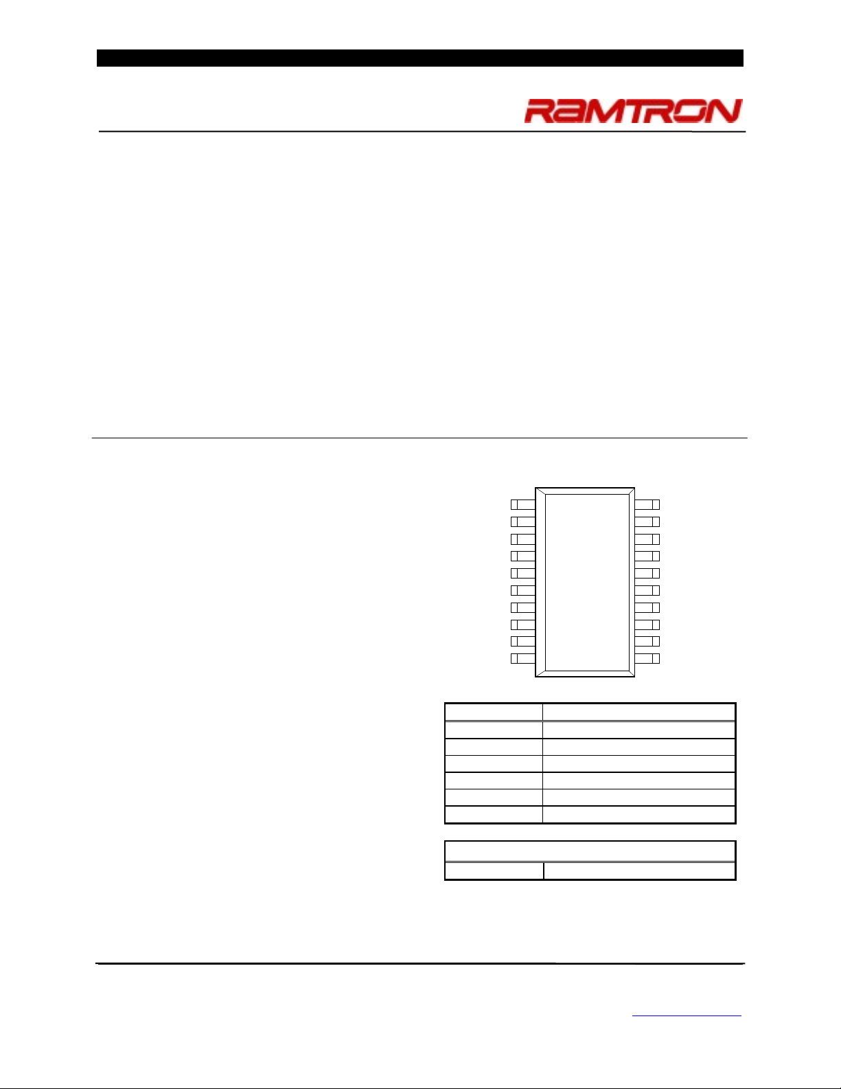
Pin Configuration
NC
NC
ACS
VDD
NC
NC
NC
NC
NC
NC
1
2
3
4
5
6
7
8
9
10
20
19
18
17
16
15
14
13
12
11
VSS
SCL
SDA
VBAK
VSS
C
C
C
Pin Name Function
ACS Alarm/Calibration/SqWave
SDA Serial Data
SCL Serial Clock
VBAK Battery-Backup Supply
VDD Supply Voltage
VSS Ground
Ordering Information
FM3135-G “Green”/RoHS 20-pin SOIC
This is a product that has fixed target specifications but are subject Ramtron International Corporation
to change pending characterization results. 1850 Ramtron Drive, Colorado Springs, CO 80921
(800) 545-FRAM, (719) 481-7000
http://www.ramtron.com
Rev. 1.1
Feb. 2008 Page 1 of 21
Page 2
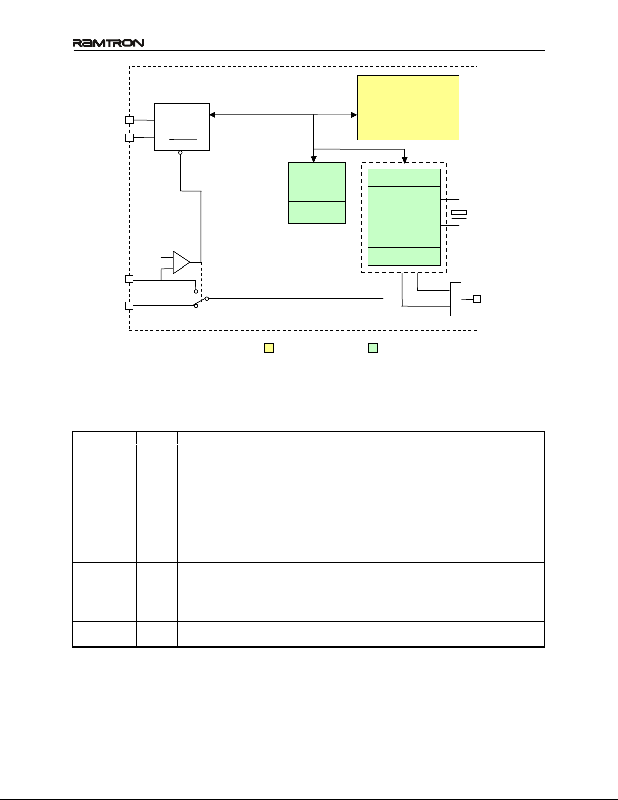
FM3135 Integrated RTC/Alarm/FRAM & Embedded Crystal
r
F-RAM
Array
SCL
SDA
2-Wire
Interface
LockOut
VDD
VBAK
Special
Function
Registers
RTC Cal.
VSW
-
+
Switched Powe
Nonvolatile
Battery Backed
RTC Registers
RTC
Alarm
Alarm
512Hz/SQW
ACS
Figure 1. Block Diagram
Pin Descriptions
Pin Name Type Pin Description
ACS Output Alarm/Calibration/SquareWave: This is an open-drain output that requires an external
pullup resistor. The alarm, calibration, and square wave functions all share this output.
In Alarm mode, this pin acts as the active-low alarm output. In Calibration mode, a 512
Hz square-wave is driven out. In SquareWave mode, the user may select a frequency of
1, 512, 4096, or 32768 Hz to be used as a continuous output. Refer to Table 3. Control
Bit Settings for ACS Pin to determine the bit settings for each mode.
SDA I/O Serial Data & Address: This is a bi-directional line for the two-wire interface. It is
open-drain and is intended to be wire-OR’d with other devices on the two-wire bus. The
input buffer incorporates a Schmitt trigger for noise immunity and the output driver
includes slope control for falling edges. A pull-up resistor is required.
SCL Input Serial Clock: The serial clock line for the two-wire interface. Data is clocked out of the
part on the falling edge, and data into the device on the rising edge. The SCL input also
incorporates a Schmitt trigger input for noise immunity.
VBAK Supply Backup supply voltage: A 3V battery or a large value capacitor. If no backup supply is
used, this pin should be tied to V
.
SS
VDD Supply Supply Voltage.
VSS Supply Ground
Rev. 1.1
Feb. 2008 Page 2 of 21
Page 3

FM3135 Integrated RTC/Alarm/FRAM & Embedded Crystal
Overview
The FM3135 device combines a serial nonvolatile
RAM with a real-time clock (RTC) and alarm. These
complementary but distinct functions share a
common interface in a single package. Although
monolithic, the product is organized as two logical
devices, the F-RAM memory and the RTC/alarm.
From the system perspective, they appear to be two
separate devices with unique IDs on the serial bus.
The memory is organized as a stand-alone 2-wire
nonvolatile memory with a standard device ID value.
The real-time clock and alarm are accessed with a
separate 2-wire device ID. This allows clock/calendar
data to be read while maintaining the most recently
used memory address. The clock and alarm are
controlled by 15 special function registers. The
registers are maintained by the power source on the
VBAK pin, allowing them to operate from battery or
backup capacitor power when V
threshold. Each functional block is described below.
drops below a set
DD
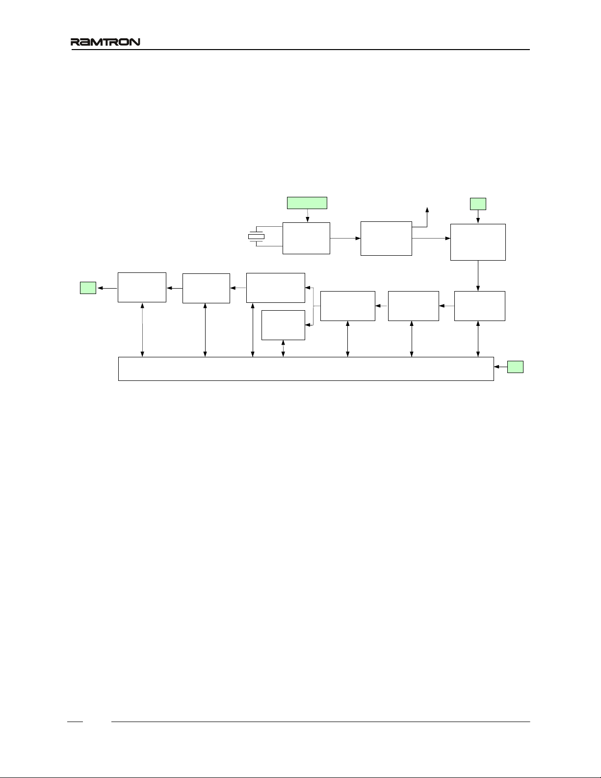
Real-Time Clock Operation
The real-time clock (RTC) is a timekeeping device
that can be battery or capacitor backed for
permanently-powered operation. It offers a software
calibration feature that allows high accuracy.
The RTC consists of an oscillator, clock divider, and
a register system for user access. It divides down the
32.768 kHz time-base and provides a minimum
resolution of seconds (1Hz). Static registers provide
the user with read/write access to the time values. It
includes registers for seconds, minutes, hours, dayof-the-week, date, months, and years. A block
diagram (Figure 2) illustrates the RTC function.
The user registers are synchronized with the
timekeeper core using R and W bits in register 00h
described below. Changing the R bit from 0 to 1
transfers timekeeping information from the core into
holding registers that can be read by the user. If a
timekeeper update is pending when R is set, then the
core will be updated prior to loading the user
Memory Operation
The FM3135 integrates a 64Kb F-RAM. The
memory is organized in bytes, 8192 addresses of 8
bits each. The memory is based on F-RAM
technology. Therefore it can be treated as RAM and
is read or written at the speed of the two-wire bus
with no delays for write operations. It also offers
effectively unlimited write endurance unlike other
nonvolatile memory technologies. The two-wire
interface protocol is described further on page 12.
The memory array can be write-protected by
software. Two bits (WP0, WP1) in register 0Eh
control the protection setting as shown in the
following table. Based on the setting, the protected
addresses cannot be written and the 2-wire interface
will not acknowledge any data to protected addresses.
The special function registers containing these bits
are described in detail below.
Table 1. F-RAM Write-Protect
Write-Protect Range WP1 WP0
None 0 0
Bottom 1/4 0 1
Bottom 1/2 1 0
Full array 1 1
The WP bits are battery-backed. On a powerup
without a backup source, the WP bits are cleared to a
‘0’ state.
registers. The registers are frozen and will not be
updated again until the R bit is cleared to ‘0’. R is
used to read the time.
Setting the W bit to ‘1’ locks the user registers.
Clearing it to a ‘0’ causes the values in the user
registers to be loaded into the timekeeper core. W is
used for writing new time values. Users should be
certain not to load invalid values, such as FFh, to the
timekeeping registers. Updates to the timekeeping
core occur continuously except when locked. All
timekeeping registers must be initialized at the first
powerup or when the LB bit is set. See the
description of the LB bit on page 11.
Backup Power
The real-time clock/calendar is intended to be
permanently powered. When the primary system
power fails, the voltage on the V
When V
is less than VSW, the RTC will switch to
DD
the backup power supply on V
pin will drop.
DD
. The clock
BAK
operates at extremely low current in order to
maximize battery or capacitor life. However, an
advantage of combining a clock function with FRAM memory is that data is not lost regardless of the
backup power source.
If a battery is applied without a V
the device has been designed to ensure the I
power supply,
DD
BAK
current does not exceed the 1µA maximum limit.
Trickle Charger
To facilitate capacitor backup the V
pin can
BAK
optionally provide a trickle charge current. When the
Rev. 1.1
Feb. 2008 Page 3 of 21
Page 4
FM3135 Integrated RTC/Alarm/FRAM & Embedded Crystal
r
VBC bit (register 0Eh, bit 2) is set to a ‘1’, the V
pin will source approximately 80 µA until V
reaches V
. This charges the capacitor to VDD
DD
without an external diode and resistor charger.
There is a Fast Charge mode which is enabled by the
FC bit (register 0Eh, bit 1). In this mode the trickle
charger current is set to approximately 1 mA,
allowing a large backup capacitor to charge more
quickly.
BAK
BAK
• In the case where no battery is used, the V
pin should be tied to V
.
SS
BAK
!
! Note: systems using lithium batteries should clear
!!
the VBC bit to 0 to prevent battery charging. The
V
circuitry includes an internal 1 KΩ series
BAK
resistor as a safety element.
512 Hz or
SW out
/OSCEN
W
32.768 kHz
crystal
CF
Months
5 bits
Years
8 bits
Date
6 bits
Days
3 bits
User Interface Registers
Figure 2. Real-Time Clock Core Block Diagram
Calibration
When the CAL bit in register 00h is set to ‘1’, the
clock enters calibration mode. In calibration mode,
the ACS output pin is dedicated to the calibration
function and the power fail output is temporarily
unavailable. Calibration operates by applying a
digital correction to the counter based on the
frequency error. In this mode, the ACS pin is driven
with a 512 Hz (nominal) square wave. Any measured
deviation from 512 Hz translates into a timekeeping
error. The user converts the measured error in ppm
and writes the appropriate correction value to the
calibration register. The correction factors are listed
in the table below. Positive ppm errors require a
negative adjustment that removes pulses. Negative
ppm errors require a positive correction that adds
pulses. Positive ppm adjustments have the CALS
(sign) bit set to ‘1’, whereas negative ppm
adjustments have CALS = 0. After calibration, the
Oscillato
Hours
6 bits
Clock
Divider
Minutes
7 bits
1 Hz
Update
Logic
Seconds
7 bits
R
clock will have a maximum error of
±
0.09 minutes per month at the calibrated
±
2.17 ppm or
temperature.
The calibration setting is battery-backed and must be
reloaded should the backup source fail. It is accessed
with bits CAL.4-0 in register 01h. This value only
can be written when the CAL bit is set to a ‘1’. To
exit the calibration mode, the user must clear the
CAL bit to a ‘0’. When the CAL bit is ‘0’, the ACS
pin will revert to another function as defined in
Table 3. Control Bit Settings for ACS Pin.
Rev. 1.1
Feb. 2008 Page 4 of 21
Page 5
FM3135 Integrated RTC/Alarm/FRAM & Embedded Crystal
Table 2. Calibration Adjustments
Measured Frequency Range Error Range (PPM)
Min Max Min Max Program Calibration Register to:
0 512.0000 511.9989 0 2.17 000000
1 511.9989 511.9967 2.18 6.51 100001
2 511.9967 511.9944 6.52 10.85 100010
3 511.9944 511.9922 10.86 15.19 100011
4 511.9922 511.9900 15.20 19.53 100100
5 511.9900 511.9878 19.54 23.87 100101
6 511.9878 511.9856 23.88 28.21 100110
7 511.9856 511.9833 28.22 32.55 100111
8 511.9833 511.9811 32.56 36.89 101000
9 511.9811 511.9789 36.90 41.23 101001
10 511.9789 511.9767 41.24 45.57 101010
11 511.9767 511.9744 45.58 49.91 101011
12 511.9744 511.9722 49.92 54.25 101100
13 511.9722 511.9700 54.26 58.59 101101
14 511.9700 511.9678 58.60 62.93 101110
15 511.9678 511.9656 62.94 67.27 101111
16 511.9656 511.9633 67.28 71.61 110000
17 511.9633 511.9611 71.62 75.95 110001
18 511.9611 511.9589 75.96 80.29 110010
19 511.9589 511.9567 80.30 84.63 110011
20 511.9567 511.9544 84.64 88.97 110100
21 511.9544 511.9522 88.98 93.31 110101
22 511.9522 511.9500 93.32 97.65 110110
23 511.9500 511.9478 97.66 101.99 110111
24 511.9478 511.9456 102.00 106.33 111000
25 511.9456 511.9433 106.34 110.67 111001
26 511.9433 511.9411 110.68 115.01 111010
27 511.9411 511.9389 115.02 119.35 111011
28 511.9389 511.9367 119.36 123.69 111100
29 511.9367 511.9344 123.70 128.03 111101
30 511.9344 511.9322 128.04 132.37 111110
31 511.9322 511.9300 132.38 136.71 111111
Positive Calibration for slow clocks: Calibration will achieve ± 2.17 PPM after calibration
Measured Frequency Range Error Range (PPM)
Min Max Min Max Program Calibration Register to:
0 512.0000 512.0011 0 2.17 000000
1 512.0011 512.0033 2.18 6.51 000001
2 512.0033 512.0056 6.52 10.85 000010
3 512.0056 512.0078 10.86 15.19 000011
4 512.0078 512.0100 15.20 19.53 000100
5 512.0100 512.0122 19.54 23.87 000101
6 512.0122 512.0144 23.88 28.21 000110
7 512.0144 512.0167 28.22 32.55 000111
8 512.0167 512.0189 32.56 36.89 001000
9 512.0189 512.0211 36.90 41.23 001001
10 512.0211 512.0233 41.24 45.57 001010
11 512.0233 512.0256 45.58 49.91 001011
12 512.0256 512.0278 49.92 54.25 001100
13 512.0278 512.0300 54.26 58.59 001101
14 512.0300 512.0322 58.60 62.93 001110
15 512.0322 512.0344 62.94 67.27 001111
16 512.0344 512.0367 67.28 71.61 010000
17 512.0367 512.0389 71.62 75.95 010001
18 512.0389 512.0411 75.96 80.29 010010
19 512.0411 512.0433 80.30 84.63 010011
20 512.0433 512.0456 84.64 88.97 010100
21 512.0456 512.0478 88.98 93.31 010101
22 512.0478 512.0500 93.32 97.65 010110
23 512.0500 512.0522 97.66 101.99 010111
24 512.0522 512.0544 102.00 106.33 011000
25 512.0544 512.0567 106.34 110.67 011001
Negative Calibration for fast clocks: Calibration will achieve ± 2.17 PPM after calibration
Rev. 1.1
Feb. 2008 Page 5 of 21
Page 6

FM3135 Integrated RTC/Alarm/FRAM & Embedded Crystal
26 512.0567 512.0589 110.68 115.01 011010
27 512.0589 512.0611 115.02 119.35 011011
28 512.0611 512.0633 119.36 123.69 011100
29 512.0633 512.0656 123.70 128.03 011101
30 512.0656 512.0678 128.04 132.37 011110
31 512.0678 512.0700 132.38 136.71 011111
Alarm
The alarm function compares user-programmed
alarm values to the corresponding RTC time/date
values. When a match occurs, an alarm event occurs.
The alarm event sets an internal flag AF (register
00h, bit 6) and drives the ACS pin low, if the
appropriate control bits are set in registers 00h and
0Eh. See Table 3. The alarm condition on the ACS
pin and the AF bit are cleared by reading register
00h.
The alarm operates under V
DD
or V
power. If the
BAK
system controller is being used to detect an alarm
while the FM3135 is powered on V
pin may cause extra I
current when the alarm is
BAK
only, the ACS
BAK
activated. To avoid battery drain, the ACS pin can be
tri-stated by reading the AF flag, located in the
RTC/Alarm Control register 00h.
There are five alarm match fields. They are Month,
Date, Hours, Minutes, and Seconds. Each of these
fields also has a Match bit that is used to determine if
the field is used in the alarm match logic. Setting the
Match bit to ‘0’ indicates that the corresponding field
will be used in the match process.
Depending on the Match bits, the alarm can occur as
specifically as one particular second on one day of
the month, or as frequently as once per second
continuously. The MSB of each Alarm register is a
Match bit. Examples of the Match bit settings are
shown in Table 4. Alarm Match Bit Examples.
Selecting none of the match bits (all ‘1’s) indicates
that no match is required. The alarm occurs every
second. Setting the match select bit for seconds to ‘0’
causes the logic to match the seconds alarm value to
the current time of day. Since a match will occur for
only one value per minute, the alarm occurs once per
minute. Likewise setting the seconds and minutes
match select bits causes an exact match of these
values. Thus, an alarm will occur once per hour.
Setting seconds, minutes, and hours causes a match
once per day. See Table 4 for other alarm setting
examples.
Function of the ACS Pin
The ACS pin is a multifunction pin. The alarm,
calibration, and square wave functions all share this
output. There are two ways a user can detect an alarm
event, by reading the AF flag or by monitoring the
ACS pin. An interrupt pin on the host processor may
be used to detect an alarm event. The AF flag in the
register 00h (bit 6) will indicate that a time/date
match has occurred. When a match occurs, the AF
bit will be set to ‘1’ and the ACS pin will drive low.
The flag and ACS pin will remain in this state until
the RTC/Alarm Control register is read which clears
the AF bit.
Table 3 that shows the relationship between register
control settings and the function of the ACS pin.
Table 3. Control Bit Settings for ACS Pin
State of Register Bit Function of
ACS pin
CAL AEN AL/SW
0 1 1 /Alarm
0 X 0 Sq Wave out
1 X X 512 Hz out
0 0 1 Hi-Z
Rev. 1.1
Feb. 2008 Page 6 of 21
Page 7
FM3135 Integrated RTC/Alarm/FRAM & Embedded Crystal
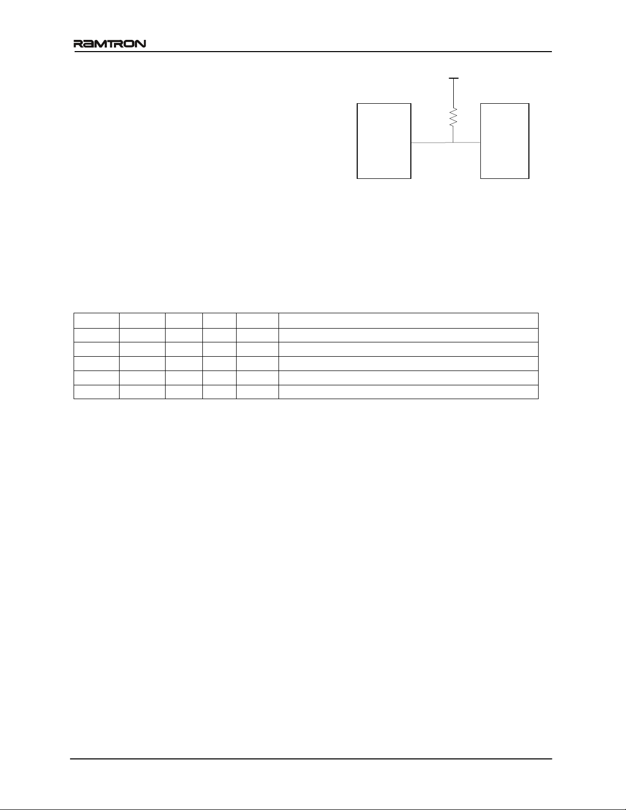
Cal Output/SquareWave Output
When the RTC calibration mode is invoked by
V
BAK
setting the CAL bit (register 00h, bit 2), the ACS
1M
output pin will be driven with a 512 Hz square wave
Ω
and the alarm will continue to operate. Since most
users only invoke the calibration mode during
production, this should have no impact on the
FM3135
ACS
otherwise normal operation of the alarm.
The ACS output may also be used to drive the system
with a continuous frequency. The AL/SW bit
(register 0Eh, bit 7) must be a ‘0’. A user-selectable
frequency is provided by F0 and F1 (register 0Eh,
bits 5 and 6). The frequencies are 1, 512, 4096, and
32768 Hz. If a continuous frequency output is
enabled by using the 512Hz or SquareWave out
functions, the alarm function will not be available.
The ACS pin is an open-drain output that needs to be
pulled up to a supply. The ACS pin and pullup
resistor draws current only when the alarm is
triggered.
Figure 4. ACS Pin Requires Pullup
Table 4. Alarm Match Bit Examples
Seconds Minutes Hours Date Months Alarm condition
1 1 1 1 1 No match required = alarm 1/second
0 1 1 1 1 Alarm when seconds match = alarm 1/minute
0 0 1 1 1 Alarm when seconds, minutes match = alarm 1/hour
0 0 0 1 1 Alarm when seconds, minutes, hours match = alarm 1/date
0 0 0 0 1 Alarm when seconds, minutes, hours, date match = alarm 1/month
MCU
Rev. 1.1
Feb. 2008 Page 7 of 21
Page 8

FM3135 Integrated RTC/Alarm/FRAM & Embedded Crystal
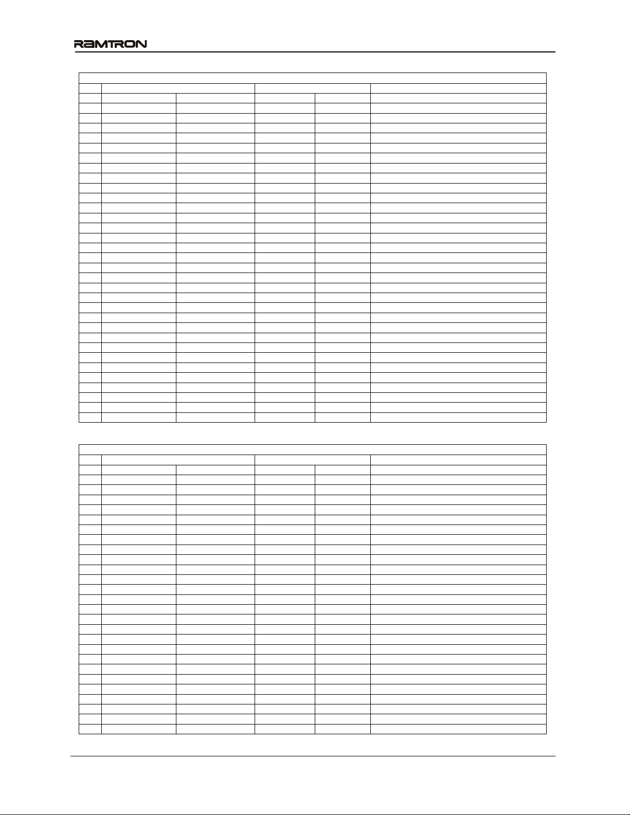
Register Map
The RTC, alarm, and other functions are accessed via 15 special function registers mapped to a separate 2-wire
device ID. The interface protocol is described below. The registers contain timekeeping data, control bits, or
information flags. A description of each register follows the summary table below.
Register Map Summary Table
Address
0Eh
0Dh
0Ch
0Bh
0Ah
09h
08h 10 years years
07h
06h
05h
04h
03h
02h
01h
00h
Note: When the device is first powered up, all registers should be treated as unknown and must be written.
Otherwise, unpredictable behavior may result.
D7 D6 D5 D4 D3 D2 D1 D0 Function Range
AL/SW F1 F0 WP1 WP0 VBC FC TST Alarm & WP Control
/Match 0 0 10 mo
/Match 0
/Match 0
/Match
/Match
00010 mo
00
00000
00
0
0
/OSCEN - CALS CAL4 CAL3 CAL2 CAL1 CAL0 CAL/Control
LB AF CF POR AEN CAL W R RTC/Alarm Control
Alarm 10 minutes Alarm minutes
Alarm 10 seconds Alarm seconds
10 date Alarm date
Alarm 10 hours Alarm hours
10 date date
10 hours hours
10 minutes minutes
10 seconds seconds
Alarm months
months
day
Alarm Month 01-12
Alarm Date 01-31
Alarm Hours 00-23
Alarm Minutes 00-59
Alarm Seconds 00-59
RTC Years
RTC Month 1-1 2
RTC Date 1-31
RTC Day 1-7
RTC Hours 0-2 3
RTC Minutes 0-59
RTC Seconds 0-59
00-99
Rev. 1.1
Feb. 2008 Page 8 of 21
Page 9

FM3135 Integrated RTC/Alarm/FRAM & Embedded Crystal
Register Description
Address Description
0Eh Alarm & WP Control
AL/SW Alarm/Square Wave Select: When set to 1, the alarm controls the ACS pin as well as the AF flag. When set to 0,
F(1:0) Square Wave Freq Select: These bits select the frequency on the ACS pin when the CAL and AL/SW bits are
WP1,WP0 Write Protect. These bits control the write protection of the memory array. Battery-backed, read/write.
VBC VBAK Charger Control: Setting VBC to 1 (and FC=0) causes approx. 80 µA (1mA if FC=1) trickle charge
FC Fast Charge: Setting FC to 1 (and VBC=1) causes approx. 1mA trickle charge current to be supplied on V
TST Invokes factory test mode. Users should always set this bit to 0.
0Dh Alarm – Month
Contains the alarm value for the month and the mask bit to select or deselect the Month value.
/M
0Ch Alarm – Date
Contains the alarm value for the date and the mask bit to select or deselect the Date value.
/M Match: Setting this bit to a ‘0’ causes the Date value to be used in the alarm match logic. Setting this bit to a ‘1’
0Bh Alarm – Hours
Contains the alarm value for the hours and the mask bit to select or deselect the Hours value.
/M Match: Setting this bit to a ‘0’ causes the Hours value to be used in the alarm match logic. Setting this bit to a ‘1’
0Ah Alarm – Minutes
Contains the alarm value for the minutes and the mask bit to select or deselect the Minutes value
/M Match: Setting this bit to a ‘0’ causes the Minutes value to be used in the alarm match logic. Setting this bit to a
D7 D6 D5 D4 D3 D2 D1 D0
AL/SW F1 F0 WP1 WP0 VBC FC TST
the selected Square Wave Freq will be driven on the ACS pin, and an alarm match only sets the AF flag. Batterybacked, read/write.
both 0. Battery-backed.
Setting F(1:0) Setting F(1:0)
1 Hz 00 (default) 4096 Hz 10
5
12 Hz
Write-Protect addresses WP1 WP0
None 0 0
Bottom 1/4 0 1
Bottom 1/2 1 0
Full array 1 1
current to be supplied on V
Clearing VBC to 0 disables the charge current. Battery-backed, read/write.
D7 D6 D5 D4 D3 D2 D1 D0
M 0 0 10 Month Month.3 Month.2 Month.1 Month.0
Match. Setting this bit to a ‘0’ causes the Month value to be used in the alarm match logic. Setting this bit to a
‘1’ causes the match circuit to ignore the Month value. Battery-backed, read/write.
D7 D6 D5 D4 D3 D2 D1 D0
M 0 10 date.1 10 date.0 Date.3 Date.2 Date.1 Date.0
causes the match circuit to ignore the Date value. Battery-backed, read/write.
D7 D6 D5 D4 D3 D2 D1 D0
M 0 10 hours.1 10 hours.0 Hours.3 Hours2 Hours.1 Hours.0
causes the match circuit to ignore the Hours value. Battery-backed, read/write.
D7 D6 D5 D4 D3 D2 D1 D0
M 10 min.2 10 min.1 10 min.0 Min.3 Min.2 Min.1 Min.0
‘1’ causes the match circuit to ignore the Minutes value. Battery-backed, read/write.
01 32768 Hz 11
. Clearing VBC to 0 disables the charge current. Battery-backed, read/write.
BAK
BAK
.
Rev. 1.1
Feb. 2008 Page 9 of 21
Page 10

FM3135 Integrated RTC/Alarm/FRAM & Embedded Crystal
09h Alarm – Seconds
Contains the alarm value for the seconds and the mask bit to select or deselect the Seconds value.
/M Match: Setting this bit to a ‘0’ causes the Seconds value to be used in the alarm match logic. Setting this bit to a
08h
Contains the lower two BCD digits of the year. Lower nibble contains the value for years; upper nibble contains
07h
Contains the BCD digits for the month. Lower nibble contains the lower digit and operates from 0 to 9; upper
06h
Contains the BCD digits for the date of the month. Lower nibble contains the lower digit and operates from 0 to 9;
05h
Lower nibble contains a value that correlates to day of the week. Day of the week is a ring counter that counts
04h
Contains the BCD value of hours in 24-hour format. Lower nibble contains the lower digit and operates from 0 to
03h
Contains the BCD value of minutes. Lower nibble contains the lower digit and operates from 0 to 9; upper nibble
02h
Contains the BCD value of seconds. Lower nibble contains the lower digit and operates from 0 to 9; upper nibble
D7 D6 D5 D4 D3 D2 D1 D0
M 10 sec.2 10 sec.1 10 sec.0 Seconds.3 Seconds.2 Seconds.1 Seconds.0
‘1’ causes the match circuit to ignore the Seconds value. Battery-backed, read/write.
Timekeeping – Years
D7 D6 D5 D4 D3 D2 D1 D0
10 year.3 10 year.2 10 year.1 10 year.0 Year.3 Year.2 Year.1 Year.0
the value for 10s of years. Each nibble operates from 0 to 9. The range for the register is 0-99. Battery-backed,
read/write.
Timekeeping – Months
D7 D6 D5 D4 D3 D2 D1 D0
0 0 0
nibble (one bit) contains the upper digit and operates from 0 to 1. The range for the register is 1-12. Batterybacked, read/write.
Timekeeping – Date of the month
D7 D6 D5 D4 D3 D2 D1 D0
0 0
upper nibble contains the upper digit and operates from 0 to 3. The range for the register is 1-31. Battery-backed,
read/write.
Timekeeping – Day of the week
D7 D6 D5 D4 D3 D2 D1 D0
0 0 0 0 0
from 1 to 7 then returns to 1. The user must assign meaning to the day value, as the day is not integrated with the
date. Battery-backed, read/write.
Timekeeping – Hours
D7 D6 D5 D4 D3 D2 D1 D0
0 0
9; upper nibble (two bits) contains the upper digit and operates from 0 to 2. The range for the register is 0-23.
Battery-backed, read/write.
Timekeeping – Minutes
D7 D6 D5 D4 D3 D2 D1 D0
0
contains the upper minutes digit and operates from 0 to 5. The range for the register is 0-59. Battery-backed,
read/write.
10 min.2 10 min.1 10 min.0 Min.3 Min.2 Min.1 Min.0
Timekeeping – Seconds
D7 D6 D5 D4 D3 D2 D1 D0
0
contains the upper digit and operates from 0 to 5. The range for the register is 0-59. Battery-backed, read/write.
10 sec.2 10 sec.1 10 sec.0 Seconds.3 Seconds.2 Seconds.1 Seconds.0
10 Month Month.3 Month.2 Month.1 Month.0
10 date.1 10 date.0 Date.3 Date.2 Date.1 Date.0
Day.2 Day.1 Day.0
10 hours.1 10 hours.0 Hours.3 Hours2 Hours.1 Hours.0
01h
/OSCEN Oscillator Enable. When set to 1, the oscillator is halted. When set to 0, the oscillator runs. Disabling the
CAL/Control
D7 D6 D5 D4 D3 D2 D1 D0
OSCEN - CALS CAL.4 CAL.3 CAL.2 CAL.1 CAL.0
oscillator can save battery power during storage. On an initial power-up of V
is internally set to 1, which turns off the oscillator. Battery-backed, read/write.
with or without V
DD
BAK
, this bit
Rev. 1.1
Feb. 2008 Page 10 of 21
Page 11

FM3135 Integrated RTC/Alarm/FRAM & Embedded Crystal
CALS Calibration Sign: Determines if the calibration adjustment is applied as an addition to or as a subtraction from
the time-base. This bit can be written only when CAL=1. Battery-backed, read/write.
CAL.4-0 Calibration Code: These five bits control the calibration of the clock. These bits can be written only when
00h
LB
AF Alarm Flag: This read-only bit is set to 1 when the time/date match the values stored in the alarm registers with
CF Century Overflow Flag: This read-only bit is set to a 1 when the values in the years register overflows from 99
POR
AEN Alarm Enable: This bit enables the alarm function. When AEN is set (and CAL cleared), the ACS pin operates
CAL Calibration Mode: When CAL is set to ‘1’, the clock enters calibration mode. When CAL is set to ‘0’, the clock
W Write RTC: Setting the W bit to ‘1’ freezes updates of the user timekeeping registers. The user can then write
R Read RTC: Setting the R bit to ‘1’ copies a static image of the timekeeping core and place it into the user
CAL=1. Battery-backed, read/write.
RTC/Alarm Control
D7 D6 D5 D4 D3 D2 D1 D0
LB AF CF POR AEN CAL W R
Low Battery Flag: If the V
will be set to ‘1’. All registers need to be re-initialized since the battery-backed register values should be
treated as unknown. The user should clear it to ‘0’ when initializing the system. Battery-backed. Read/Write
(internally set, user can clear bit by writing to a ‘0’).
the Match bit(s) = 0. It is cleared when the RTC/Alarm Control register is read. Battery-backed.
to 00. This indicates a new century, such as going from 1999 to 2000 or 2099 to 2100. The user should record
the new century information as needed. This bit is cleared when the RTC/Alarm Control register is read.
Battery-backed.
Power On Reset Flag: When V
Read/Write (internally set, user can clear bit by writing to a ‘0’).
as an active-low alarm and the AF flag function is enabled. The function of the ACS pin is detailed in Table 3.
When AEN is cleared, no new alarm events will occur but the AF flag and ACS pin will not be cleared.
Battery-backed, read/write.
operates normally, and the ACS pin is controlled by the RTC alarm. Battery-backed, read/write.
them with updated values. Setting the W bit to ‘0’ causes the contents of the time registers to be transferred to
the timekeeping counters. Battery-backed, read/write.
registers. The user can then read them without concerns over changing values causing system errors. The R bit
going from ‘0’ to ‘1’ causes the timekeeping capture, so the bit must be returned to ‘0’ prior to reading again.
Battery-backed, read/write.
source drops to a voltage level insufficient to operate the RTC/alarm, this bit
BAK
drops below VSW, the POR bit will be set to ‘1’. Battery-backed.
DD
Rev. 1.1
Feb. 2008 Page 11 of 21
Page 12
FM3135 Integrated RTC/Alarm/FRAM & Embedded Crystal
Two-wire Interface
The FM3135 employs an industry standard two-wire
bus that is familiar to many users. This product is
unique since it incorporates two logical devices in
one chip. Each logical device can be accessed
individually. Although monolithic, it appears to the
system software to be two separate products. One is
a memory device. It has a Slave Address (Slave ID =
1010b) that operates the same as a stand-alone
memory device. The second device is a real-time
clock and alarm which have a unique Slave Address
(Slave ID = 1101b).
By convention, any device that is sending data onto
the bus is the transmitter while the target device for
this data is the receiver. The device that is
controlling the bus is the master. The master is
responsible for generating the clock signal for all
operations. Any device on the bus that is being
controlled is a slave. The FM3135 is always a slave
device.
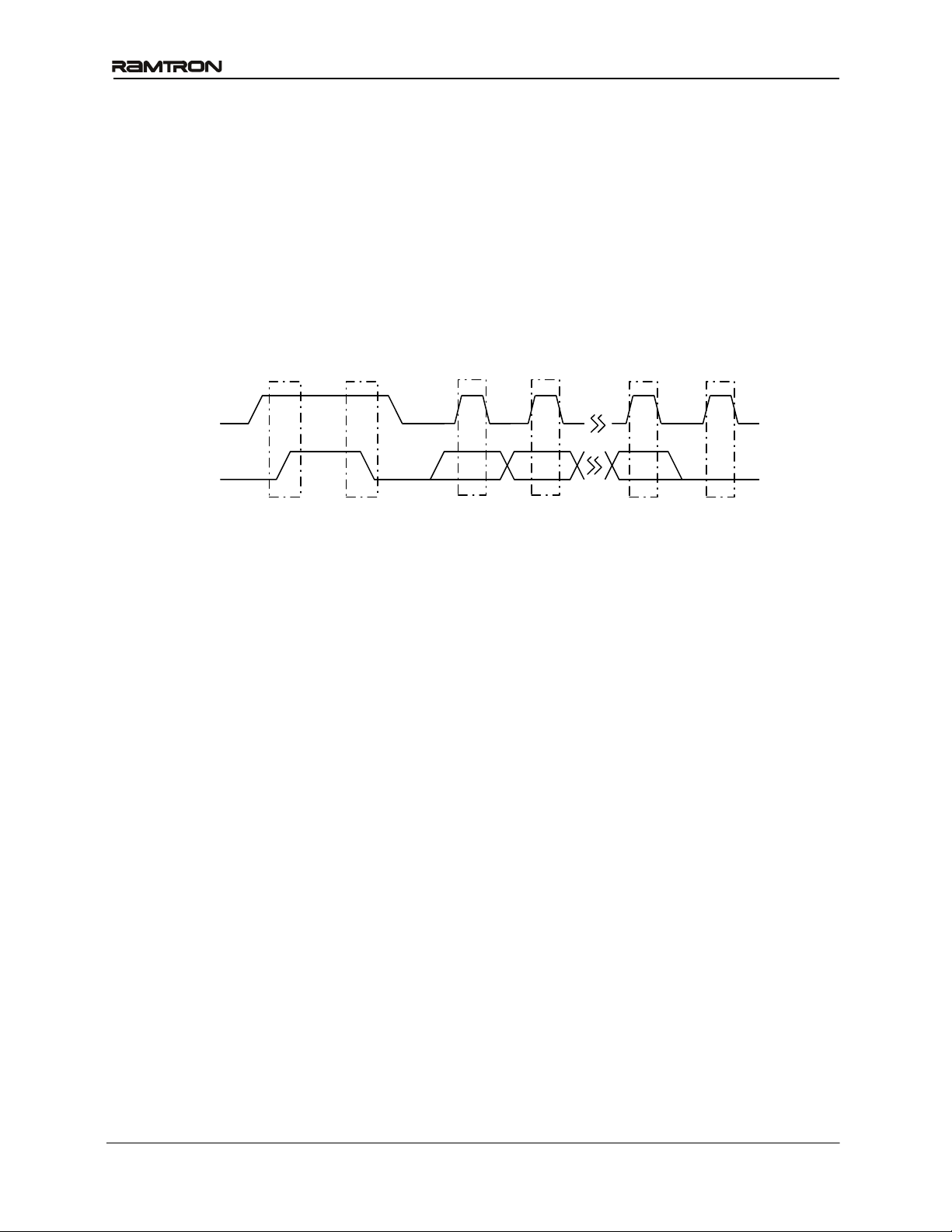
The bus protocol is controlled by transition states in
the SDA and SCL signals. There are four conditions:
Start, Stop, Data bit, and Acknowledge. The figure
below illustrates the signal conditions that specify
the four states. Detailed timing diagrams are shown
in the Electrical Specifications section.
SCL
SDA
Stop
(Master)
Start
(Master)
Figure 4. Data Transfer Protocol
Start Condition
A Start condition is indicated when the bus master
drives SDA from high to low while the SCL signal is
high. All read and write transactions begin with a
Start condition. An operation in progress can be
aborted by asserting a Start condition at any time.
Aborting an operation using the Start condition will
ready the FM3135 for a new operation.
Stop Condition
A Stop condition is indicated when the bus master
drives SDA from low to high while the SCL signal is
high. All operations must end with a Stop condition.
If an operation is pending when a stop is asserted,
the operation will be aborted. The master must have
control of SDA (not a memory read) in order to
assert a Stop condition.
Data/Address Transfer
All data transfers (including addresses) take place
while the SCL signal is high. Except under the two
conditions described above, the SDA signal should
not change while SCL is high.
Acknowledge
The Acknowledge (ACK) takes place after the 8
th
data bit has been transferred in any transaction.
7
Data bits
(Transmitter)
During this state the transmitter must release the
SDA bus to allow the receiver to drive it. The
receiver drives the SDA signal low to acknowledge
receipt of the byte. If the receiver does not drive
SDA low, the condition is a No-Acknowledge
(NACK) and the operation is aborted.
The receiver might NACK for two distinct reasons.
First is that a byte transfer fails. In this case, the
NACK ends the current operation so that the part can
be addressed again. This allows the last byte to be
recovered in the event of a communication error.
Second and most common, the receiver does not
send an ACK to deliberately terminate an operation.
For example, during a read operation, the FM3135
will continue to place data onto the bus as long as the
receiver sends ACKs (and clocks). When a read
operation is complete and no more data is needed,
the receiver must NACK the last byte. If the receiver
ACKs the last byte, this will cause the FM3135 to
attempt to drive the bus on the next clock while the
master is sending a new command such as a Stop.
Slave Address
The first byte that the FM3135 expects after a Start
condition is the slave address. As shown in figures
below, the slave address contains the Slave ID and a
bit that specifies if the transaction is a read or a
write.
6
0
Data bit
(Transmitter)
Acknowledge
(Receiver)
Rev. 1.1
Feb. 2008 Page 12 of 21
Page 13

FM3135 Integrated RTC/Alarm/FRAM & Embedded Crystal
The FM3135 has two Slave Addresses (Slave IDs)
associated with two logical devices. To access the
memory device, bits 7-4 should be set to 1010b. The
other logical device within the FM3135 is the realtime clock and alarm. To access this device, bits 7-4
of the slave address should be set to 1101b. A bus
transaction with this slave address will not affect the
memory in any way. The figures below illustrate the
two Slave Addresses.
Bits 3 through 1 of the Slave Address must be logic
0. Bit 0 is the read/write bit. A ‘1’ indicates a read
operation, and a ‘0’ indicates a write operation.
address. A random read address can be loaded by
beginning a write operation as explained below.
After transmission of each data byte, just prior to the
Acknowledge, the FM3135 increments the internal
address. This allows the next sequential byte to be
accessed with no additional addressing externally.
After the last address is reached, the address latch
will roll over to 0000h. There is no limit to the
number of bytes that can be accessed with a single
read or write operation.
Addressing Overview – RTC/Alarm
The RTC/Alarm operates in a similar manner to the
Slave ID
memory, except that it uses only one byte of address.
Addresses 00h to 0Eh correspond to the RTC/Alarm
and control registers. Attempting to load addresses
0
1
0
1
0
0
7
6 5
4
3
2
R/W
0
1
0
Figure 5. Slave Address – Memory
Slave ID
above 0Eh is an illegal condition; the FM3135 will
return a NACK and abort the 2-wire transaction.
Data Transfer
After the address information has been transmitted,
data transfer between the bus master and the
FM3135 begins. For a read, the FM3135 will place 8
data bits on the bus then wait for an ACK from the
1
1
0
1
0
0
7
6 5
4
3
2
R/W
0
1
0
Figure 6. Slave Address – RTC
Addressing Overview – Memory
After the FM3135 acknowledges the Slave Address,
the master can place the memory address on the bus
for a write operation. The address requires two bytes.
The first is the MSB (upper byte). The first 3 unused
address bits are don’t cares, but should be set to ‘0’
to maintain upward compatibility. Following the
MSB is the LSB (lower byte) which contains the
remaining eight address bits. The address is latched
internally. Each access causes the latched address to
be incremented automatically. The current address is
the value that is held in the latch, either a newly
written value or the address following the last access.
The current address will be held as long as V
greater than V
or until a new value is written.
SW
DD
is
Accesses to the clock do not affect the current
memory address. Reads always use the current
master. If the ACK occurs, the FM3135 will transfer
the next byte. If the ACK is not sent, the FM3135
will end the read operation. For a write operation, the
FM3135 will accept 8 data bits from the master then
send an Acknowledge. All data transfer occurs MSB
(most significant bit) first.
Memory Write Operation
All memory writes begin with a Slave Address, then
a memory address. The bus master indicates a write
operation by setting the slave address LSB to a ‘0’.
After addressing, the bus master sends each byte of
data to the memory and the memory generates an
Acknowledge condition. Any number of sequential
bytes may be written. If the end of the address range
is reached internally, the address counter will wrap
to 0000h. Internally, the actual memory write occurs
after the 8
th
data bit is transferred. It will be complete
before the Acknowledge is sent. Therefore, if the
user desires to abort a write without altering the
memory contents, this should be done using a Start
or Stop condition prior to the 8
th
data bit. The figures
below illustrate a single- and multiple-writes to
memory.
Rev. 1.1
Feb. 2008 Page 13 of 21
Page 14

FM3135 Integrated RTC/Alarm/FRAM & Embedded Crystal
A
A
A
A
A
A
A
A
A
A
A
A
By Master
Start
S
Slave Ad dr ess
0
Address MSB
ddress & Data
ddress LSB
Data Byte
Stop
P
By FM3130
Figure 7. Single Byte Memory Write
Start
By Maste r
By FM3130
Address & Data
Address MSB
Acknowledge
S
Slave Address
0
Figure 8. Multiple Byte Memory Write
Memory Read Operation
There are two types of memory read operations. They
are current address read and selective address read. In
a current address read, the FM3135 uses the internal
address latch to supply the address. In a selective
read, the user performs a procedure to first set the
address to a specific value.
Current Address & Sequential Read
As mentioned above the FM3135 uses an internal
latch to supply the address for a read operation. A
current address read uses the existing value in the
address latch as a starting place for the read
operation. The system reads from the address
immediately following that of the last operation.
To perform a current address read, the bus master
supplies a slave address with the LSB set to 1. This
indicates that a read operation is requested. After
receiving the complete device address, the FM3135
will begin shifting data out from the current address
on the next clock. The current address is the value
held in the internal address latch.
Beginning with the current address, the bus master
can read any number of bytes. Thus, a sequential read
is simply a current address read with multiple byte
transfers. After each byte the internal address counter
will be incremented.
Each time the bus master acknowledges a byte,
this indicates that the FM3135 should read out
the next sequential byte.
cknowledge
Address LSB
Data Byte
Data Byte
There are four ways to terminate a read operation.
Failing to properly terminate the read will most likely
create a bus contention as the FM3135 attempts to
read out additional data onto the bus. The four valid
methods follow.
1. The bus master issues a NACK in the 9
cycle and a Stop in the 10
th
clock cycle. This is
illustrated in the diagrams below and is
preferred.
2. The bus master issues a NACK in the 9
cycle and a Start in the 10
th
.
3. The bus master issues a Stop in the 9
cycle.
4. The bus master issues a Start in the 9
cycle.
If the internal address reaches the top of memory, it
will wrap around to 0000h on the next read cycle.
The figures below show the proper operation for
current address reads.
Selective (Random) Read
There is a simple technique that allows a user to
select a random address location as the starting point
for a read operation. This involves using the first
three bytes of a write operation to set the internal
address followed by subsequent read operations.
To perform a selective read, the bus master sends out
the slave address with the LSB set to 0. This specifies
a write operation. According to the write protocol,
the bus master then sends the address bytes that are
loaded into the internal address latch. After the
FM3135 acknowledges the address, the bus master
Stop
th
clock
th
clock
th
clock
th
clock
P
Rev. 1.1
Feb. 2008 Page 14 of 21
Page 15

FM3135 Integrated RTC/Alarm/FRAM & Embedded Crystal
A
A
A
A
A
issues a Start condition. This simultaneously aborts
the write operation and allows the read command to
be issued with the slave address LSB set to a ‘1’. The
operation is now a read from the current address.
Read operations are illustrated below.
RTC/Alarm Write Operation
All RTC/Alarm writes operate in a similar manner to
memory writes. The distinction is that a different
device ID is used and only one byte address is needed
instead of two. Figure 12 illustrates a single byte
write to the RTC/Alarm.
RTC/Alarm Read Operation
As with writes, a read operation begins with the
Slave Address. To perform a register read, the bus
master supplies a Slave Address with the LSB set to a
‘1’. This indicates that a read operation is requested.
After receiving the complete Slave Address, the
FM3135 will begin shifting data out from the current
register address on the next clock. Auto-increment
operates for the special function registers as with the
memory address. A current address read for the
registers look exactly like the memory except that the
device ID is different.
The FM3135 contains two separate address registers,
one for the memory address and the other for the
register address. This allows the contents of one
address register to be modified without affecting the
current address of the other register. For example,
this would allow an interrupted read to the memory
while still providing fast access to an RTC register. A
subsequent memory read will then continue from the
memory address where it previously left off, without
requiring the load of a new memory address.
However, a write sequence always requires an
address to be supplied.
By Master
Start
ddress
No
cknowledge
Stop
By FM3130
By Master
By FM3130
By Master
Start
S A
Slave Address
Start
S
Slave Addr ess
S
1
cknowledge
Data Byte
Data
1 P
Figure 9. Current Address Memory Read
No
Address
Acknowledge
Acknowledge
ASlave Address 1 Data Byte 1 P
Data
Data ByteA
cknowledge
Stop
Figure 10. Sequential Memory Read
Address
0
Address MSB
A
Address LSB
Start Address
S A
A
Slave Address
1
Data Byte
No
Acknowledge
Stop
1 P
By FM3130
Acknowledge
Data
Figure 11. Selective (Random) Memory Read
Rev. 1.1
Feb. 2008 Page 15 of 21
Page 16

FM3135 Integrated RTC/Alarm/FRAM & Embedded Crystal
By Master
Start
Address & Data
Stop
By FM3135
S
Slave Address
A
0 A
0 0 0
0
Address
Acknowledge
Data Byte
Figure 12. Register Byte Write
* Although not required, it is recommended that A7-A4 in the Register Address byte are
zeros in order to preserve compatibility with future devices.
A P
Rev. 1.1
Feb. 2008 Page 16 of 21
Page 17

FM3135 Integrated RTC/Alarm/FRAM & Embedded Crystal
Electrical Specifications
Absolute Maximum Ratings
Symbol Description Ratings
VDD Power Supply Voltage with respect to VSS -1.0V to +5.0V
VIN Voltage on any signal pin with respect to VSS -1.0V to +5.0V * and
V
≤ VDD+1.0V **
IN
V
Backup Supply Voltage -1.0V to +4.5V
BAK
T
Storage Temperature
STG
T
Lead Temperature (Soldering, 10 seconds)
LEAD
V
Electrostatic Discharge Voltage
ESD
- Human Body Model
- Charged Device Model
(JEDEC Std JESD22-A114-B)
(JEDEC Std JESD22-C101-A)
- Machine Model (JEDEC Std JESD22-A115-A)
-55°C to + 125°C
300° C
4kV
1kV
200V
Package Moisture Sensitivity Level TBD
** The “VIN < VDD+1.0V” restriction does not apply to the SCL, SDA, and ACS pins which do not employ a diode to VDD.
Stresses above those listed under Absolute Maximum Ratings may cause permanent damage to the device. This is a stress rating only,
and the functional operation of the device at these or any other conditions above those listed in the operational section of this
specification is not implied. Exposure to absolute maximum ratings conditions for extended periods may affect device reliability.
DC Operating Conditions (
T
= -40° C to + 85° C, V
A
= 2.7V to 3.6V unless otherwise specified)
DD
Symbol Parameter Min Typ Max Units Notes
VDD Main Power Supply 2.7 - 3.6 V 1
IDD VDD Supply Current
@ SCL = 100 kHz
@ SCL = 1 MHz
ISB Standby Current
Trickle Charger Off
Trickle Chrg On, Fast Chrg Off
Trickle Chrg On, Fast Chrg On
V
RTC Backup Supply Voltage 2.0 3.0 3.6 V 4
BAK
I
RTC Backup Supply Current 1
BAK
I
Trickle Charge Current with V
BAKTC
(VBC=0)
(VBC=1, FC=0)
(VBC=1, FC=1)
=0V
BAK
Fast Charge Off (FC = 0)
Fast Charge On (FC = 1)
ILI Input Leakage Current
ILO Output Leakage Current
VIH Input High Voltage 0.7 VDD V
VIL Input Low Voltage -0.3 0.3 V
V
Output Low Voltage (IOL = 3 mA)
OL1
150
500
50
190
2600
25
200
120
2500
±1 µA
±1 µA
+ 0.3 V
DD
DD
- 0.4 V
µA
µA
µA
µA
µA
µA
µA
µA
V
2
3
5
6
7
7
- Applies to SDA and ACS pin
- V
> VSW
DD
V
OL2
Output Low Voltage (I
- Applies only to ACS pin
- V
applied, VDD < VSW
BAK
= 80 µA)
OL
-
0.4
V
VSW Battery Switchover Voltage 2.0 2.7 V
Notes
1.
Full complete operation. RTC operates to lower voltages as specified.
2.
SCL toggling between VDD-0.3V and VSS, other inputs VSS or VDD-0.3V. VBC=0. IDD is linear vs frequency.
3.
All inputs at VSS or V
4.
The VBAK trickle charger automatically regulates the maximum voltage on this pin for capacitor backup applications.
5.
V
= 3.0V, VDD < VSW, oscillator running.
BAK
6.
V
will source current when the trickle charger is enabled (VBC=1), VDD > V
BAK
7.
VIN or V
= VSS to VDD.
OUT
static. Stop command issued.
DD,
and VDD > VSW.
BAK
Rev. 1.1
Feb. 2008 Page 17 of 21
Page 18

FM3135 Integrated RTC/Alarm/FRAM & Embedded Crystal
AC Parameters
(T
= -40° C to + 85° C, V
A
= 2.7V to 3.6V, CL = 100 pF unless otherwise specified)
DD
Symbol Parameter Min Max Min Max Min Max Units Notes
f
SCL Clock Frequency 0 100 0 400 0 1000 kHz
SCL
t
Clock Low Period 4.7 1.3 0.6
LOW
t
Clock High Period 4.0 0.6 0.4
HIGH
tAA SCL Low to SDA Data Out Valid 3 0.9 0.55
t
Bus Free Before New Transmission 4.7 1.3 0.5
BUF
t
Start Condition Hold Time 4.0 0.6 0.25
HD:STA
t
Start Condition Setup for Repeated
SU:STA
4.7 0.6 0.25
µs
µs
µs
µs
µs
µs
Start
t
Data In Hold Time 0 0 0 ns
HD:DAT
t
Data In Setup Time 250 100 100 ns
SU:DAT
tR Input Rise Time 1000 300 300 ns 1
tF Input Fall Time 300 300 100 ns 1
t
Stop Condition Setup Time 4.0 0.6 0.25
SU:STO
tDH Data Output Hold
tSP Noise Suppression Time Constant
(from SCL @ VIL)
0 0 0 ns
50 50 50 ns
µs
on SCL, SDA
All SCL specifications as well as start and stop conditions apply to both read and write operations.
Supervisor Timing
(T
= -40° C to + 85° C, V
A
= 2.7V to 3.6V)
DD
Symbol Parameter Min Max Units Notes
tVR V
tVF V
t
Device active after VDD>2.7V - 20 ms
RPU
Capacitance
Rise Time 50 -
DD
Fall Time 100 -
DD
(T
= 25° C, f=1.0 MHz, V
A
= 3.0V)
DD
µs/V
µs/V
1,2
1,2
Symbol Parameter Typ Max Units Notes
CIO Input/Output Capacitance - 8 pF 1
Notes
1 This parameter is characterized but not tested.
2 Slope measured at any point on V
Data Retention
(T
= -40° C to + 85° C, V
A
waveform.
DD
DD
= 2.7V to 3.6V)
Parameter Min Units Notes
Data Retention 10 Years
Rev. 1.1
Feb. 2008 Page 18 of 21
Page 19

FM3135 Integrated RTC/Alarm/FRAM & Embedded Crystal
AC Test Conditions Equivalent AC Test Load Circuit
Input Pulse Levels 0.1 V
to 0.9 VDD
DD
3.6V
Input rise and fall times 10 ns
Input and output timing levels 0.5 V
DD
1100
Ω
Diagram Notes
All start and stop timing parameters apply to both read and write
cycles. Clock specifications are identical for read and write cycles.
Write timing parameters apply to slave address, word address, and
Output
100 pF
write data bits. Functional relationships are illustrated in the relevant
data sheet sections. These diagrams illustrate the timing parameters
only.
Read Bus Timing
t
t
R
HIGH
t
F
`
t
LOW
t
SP
t
SP
SCL
1/f
SCL
t
t
AA
DH
t
HD:DAT
t
SU:DAT
Acknowledge
SDA
t
SU:STA
Start
t
BUF
Stop Start
Write Bus Timing
t
HD:DAT
SCL
t
SU:STO
t
HD:STA
t
SU:DAT
t
AA
SDA
Start
Stop Start Acknowledge
Power Cycle Timing
VDD
2.7V
t
RPU
Can user
access device?
yes
no
yes
Rev. 1.1
Feb. 2008 Page 19 of 21
Page 20

α
FM3135 Integrated RTC/Alarm/FRAM & Embedded Crystal
Mechanical Drawing
20-pin SOIC (JEDEC Standard MS-013d variation AC)
h
°
45
Seating Plane
0.10 mm
L
C
Pin 1
E H
D
A
e
B
A1
Refer to JEDEC MS-013 for complete dimensions and notes.
All dimensions in millimeter s
.
Symbol Dim Min Nom. Max
A mm 2.35 2.65
A1 mm 0.10 0.30
B mm 0.33 0.51
C mm 0.23 0.32
D mm 12.8 BSC
E mm 7.40 7.60
e mm
in.
1.27 BSC
0.050 BSC
H mm 10.00 10.65
h mm 0.25 0.75
L mm 0.40 1.27
α
0°
8°
SOIC Package Marking Scheme
Legend:
XXXX= part number, P= package type
LLLLLLL= lot code
XXXXXXX-P
RIC=Ramtron Int’l Corp, YY=year, WW=work week
LLLLLLL
RICYYWW
Example: FM3135, “Green” SOIC package, Year 2007, Work Week 14
FM3135-G
A70003G
RIC0714
Rev. 1.1
Feb. 2008 Page 20 of 21
Page 21

FM3135 Integrated RTC/Alarm/FRAM & Embedded Crystal
Revision History
Revision
0.1 12/14/2006 Initial release.
1.0 12/19/2007 Changed to Preliminary status. Changed pinout. Added ESD ratings.
1.1 2/29/2008 Updated ESD ratings.
Date
Summary
Rev. 1.1
Feb. 2008 Page 21 of 21
 Loading...