

Page 1

1
www.fairchildsemi.com
FM25C640U Rev. B
FM25C640U 64K-Bit SPI Interface Serial CMOS EEPROM
FM25C640U
64K-Bit SPI™ Interface
Serial CMOS EEPROM
Block Diagram
February 2002
© 2002 Fairchild Semiconductor Corporation
Instruction
Decoder
Control Logic
and Clock
Generators
High Voltage
Generator
and
Program
Timer
Instruction
Register
Program
Enable
Data In/Out Register
8 Bits
Data Out
Buffer
Non-Volatile
Status Register
Decoder
Address
Counter/
Register
EEPROM Array
Read/Write Amps
/CS
/HOLD
SCK
V
CC
V
SS
V
PP
/WP
SI
SO
General Description
The FM25C640U is a 64K bit serial interface CMOS EEPROM
(Electrically Erasable Programmable Read-Only Memory). This
device fully conforms to the SPI 4-wire protocol which uses Chip
Select (/CS), Clock (SCK), Data-in (SI) and Data-out (SO) pins to
synchronously control data transfer between the SPI microcontroller
and the EEPROM. In addition, the serial interface allows a minimal
pin count, packaging designed to simplify PC board layout requirements and offers the designer a variety of low voltage and low
power options.
This SPI EEPROM family is designed to work with the 68HC11 or
any other SPI-compatible, high-speed microcontroller and offers
both hardware (/WP pin) and software ("block write") data protection. For example, entering a 2-bit code into the STATUS REGISTER prevents programming in a selected block of memory and all
programming can be inhibited by connecting the /WP pin to VSS;
allowing the user to protect the entire array or a selected section.
In addition, SPI devices feature a /HOLD pin, which allows a
temporary interruption of the datastream into the EEPROM.
Fairchild EEPROMs are designed and tested for applications
requiring high endurance, high reliability, and low power consumption for a continuously reliable non-volatile solution for all
markets.
Functions
■ SPI MODE 0 interface
■ 64K bits organized as 8K x 8
■ Extended 2.7V to 5.5V operating voltage
■ 2.1 MHz operation @ 4.5V - 5.5V
■ Self-timed programming cycle
■ "Programming complete" indicated by STATUS REGISTER
polling
■ /WP pin and BLOCK WRITE protection
Features
■ Sequential read of entire array
■ 32 byte "Page write" mode to minimize total write time per
byte
■ /WP pin and BLOCK WRITE protection to prevent inadvertent programming as well as programming ENABLE and
DISABLE opcodes.
■ /HOLD pin to suspend data transfer
■ Typical 1µA standby current (ISB) for "L" devices and 0.1µA
standby current for "LZ" devices.
■ Endurance: Up to 1,000,000 data changes
■ Data retention greater than 40 years
SPI™ is a trademark of Motorola Corporation
Page 2

2
www.fairchildsemi.com
FM25C640U Rev. B
FM25C640U 64K-Bit SPI Interface Serial CMOS EEPROM
Connection Diagram
Dual-In-Line Package (N) and SO Package (M8)
Top View
See Package Number N08E (N) and M08A (M8)
Pin Names
/CS Chip Select Input
SO Serial Data Output
/WP Write Protect
V
SS
Ground
SI Serial Data Input
SCK Serial Clock Input
/HOLD Suspends Serial Data
V
CC
Power Supply
Ordering Information
FM 25 C XX U LZ E XX Letter Description
Package N 8-pin DIP
M8 8-pin SO
Temp. Range None 0 to 70°C
V -40 to +125°C
E -40 to +85°C
Voltage Operating Range Blank 4.5V to 5.5V
L 2.7V to 5.5V
LZ 2.7V to 5.5V and
<1µA Standby Current
Ultralite CS100UL Process
Density/Mode 640 64K, mode 0
C CMOS technology
Interface 25 SPI
FM Fairchild Nonvolatile
Memory Prefix
/CS
SO
/WP
V
SS
V
CC
/HOLD
SCK
SI
8
7
6
5
1
2
3
4
FM25C640U
Page 3

3
www.fairchildsemi.com
FM25C640U Rev. B
FM25C640U 64K-Bit SPI Interface Serial CMOS EEPROM
Standard Voltage 4.5 ≤ VCC ≤ 5.5V Specifications
Absolute Maximum Ratings (Note 1)
Ambient Storage Temperature -65°C to +150°C
All Input or Output Voltage with
Respect to Ground +6.5V to -0.3V
Lead Temp. (Soldering, 10 sec.) +300°C
ESD Rating 2000V
Operating Conditions
Ambient Operating Temperature
FM25C640U 0°C to +70°C
FM25C640UE -40°C to +85°C
FM25C640UV -40°C to +125°C
Power Supply (VCC) 4.5V to 5.5V
DC and AC Electrical Characteristics 4.5V ≤ V
CC
≤ 5.5V (unless otherwise specified)
Symbol Parameter Conditions Min Max Units
I
CC
Operating Current /CS = V
IL
3mA
I
CCSB
Standby Current /CS = V
CC
50 µA
I
IL
Input Leakage VIN = 0 to V
CC
-1 +1 µA
I
OL
Output Leakage V
OUT
= GND to V
CC
-1 +1 µA
V
IL
CMOS Input Low Voltage -0.3 VCC * 0.3 V
V
IH
CMOS Input High Voltage 0.7 * VCCVCC + 0.3 V
V
OL
Output Low Voltage IOL = 1.6 mA 0.4 V
V
OH
Output High Voltage IOH = -0.8 mA VCC - 0.8 V
f
OP
SCK Frequency 2.1 MHz
t
RI
Input Rise Time 2.0 µs
t
FI
Input Fall Time 2.0 µs
t
CLH
Clock High Time (Note 2) 190 ns
t
CLL
Clock Low Time (Note 2) 190 ns
t
CSH
Min /CS High Time (Note 3) 240 ns
t
CSS
/CS Setup Time 240 ns
t
DIS
Data Setup Time 100 ns
t
HDS
/HOLD Setup Time 90 ns
t
CSN
/CS Hold Time 240 ns
t
DIN
Data Hold Time 100 ns
t
HDN
/HOLD Hold Time 90 ns
t
PD
Output Delay CL = 200 pF 240 ns
t
DH
Output Hold Time 0 ns
t
LZ
/HOLD to Output Low Z 100 ns
t
DF
Output Disable Time CL = 200 pF 240 ns
t
HZ
/HOLD to Output High Z 100 ns
t
WP
Write Cycle Time 1–16 Bytes 10 ms
Capacitance T
A
= 25°C, f = 2.1/1 MHz (Note 4)
Symbol Test Typ Max Units
C
OUT
Output Capacitance 3 8 pF
C
IN
Input Capacitance 2 6 pF
AC Test Conditions
Output Load CL = 200 pF
Input Pulse Levels 0.1 * VCC – 0.9 * V
CC
Timing Measurement Reference Level 0.3 * VCC - 0.7 * V
CC
Note 1: Stress above those listed under “Absolute Maximum Ratings” may cause permanent damage to the device. This is a stress rating only, and functional operation of the
device at these or any other conditions above those indicated in the operational sections of the specification is not implied. Exposure to absolute maximum rating conditions for
extended periods may affect device reliability.
Note 2: The fOP frequency specification specifies a minimum clock period of 1/fOP. Therefore, for every fOP clock cycle, t
CLH
+ t
CLL
must be equal to or greater than 1/fOP. For
example, for a fOP of 2.1MHz, the period equals 476ns. In this case if t CLH = is set to 190ns, then t
CLL
must be set to a minimum of 286ns.
Note 3: /CS must be brought high for a minimum of t
CSH
between consecutive instruction cycles.
Note 4: This parameter is periodically sampled and not 100% tested.
Page 4

4
www.fairchildsemi.com
FM25C640U Rev. B
FM25C640U 64K-Bit SPI Interface Serial CMOS EEPROM
Low Voltage 2.7V ≤ VCC ≤ 4.5V Specifications
Absolute Maximum Ratings (Note 5)
Ambient Storage Temperature -65°C to +150°C
All Input or Output Voltage with
Respect to Ground +6.5V to -0.3V
Lead Temp. (Soldering, 10 sec.) +300°C
ESD Rating 2000V
Operating Conditions
Ambient Operating Temperature
FM25C640UL/LZ 0°C to +70°C
FM25C640ULE/LZE -40°C to +85°C
FM25C640ULV -40°C to +125°C
Power Supply (V
CC
) 2.7V–4.5V
DC and AC Electrical Characteristics 2.7V ≤ V
CC
≤ 4.5V (unless otherwise specified)
25C640UL/LE 25C640ULV
25C640ULZ/ZE
Symbol Parameter Part Conditions Min. Max. Min Max Units
I
CC
Operating Current /CS = V
IL
33mA
I
CCSB
Standby Current L /CS = V
CC
10 10 µA
LZ 1 N/A µA
I
IL
Input Leakage VIN = 0 to V
CC
-1 1 -1 1 µA
I
OL
Output Leakage V
OUT
= GND to V
CC
-1 1 -1 1 µA
V
IL
Input Low Voltage -0.3 VCC * 0.3 -0.3 VCC * 0.3 V
V
IH
Input High Voltage VCC * 0.7 VCC + 0.3 VCC * 0.7 VCC + 0.3 V
V
OL
Output Low Voltage I
OL
= 0.8 mA 0.4 0.4 V
V
OH
Output High Voltage I
OH
= –0.8 mA VCC - 0.8 VCC - 0.8 V
f
OP
SCK Frequency 1.0 1.0 MHz
t
RI
Input Rise Time 2.0 2.0 µs
t
FI
Input Fall Time 2.0 2.0 µs
t
CLH
Clock High Time (Note 6) 410 410 ns
t
CLL
Clock Low Time (Note 6) 410 410 ns
t
CSH
Min. /CS High Time (Note 7) 500 500 ns
t
CSS
/CS Setup Time 500 500 ns
t
DIS
Data Setup Time 100 100 ns
t
HDS
/HOLD Setup Time 240 240 ns
t
CSN
/CS Hold Time 500 500 ns
t
DIN
Data Hold Time 100 100 ns
t
HDN
/HOLD Hold Time 240 240 ns
t
PD
Output Delay CL = 200 pF 500 500 ns
t
DH
Output Hold Time 0 0 ns
t
LZ
/HOLD Output Low Z 240 240 ns
t
DF
Output Disable Time CL = 200 pF 500 500 ns
t
HZ
/HOLD to Output Hi Z 240 240 ns
t
WP
Write Cycle Time 1-16 Bytes 15 15 ms
Capacitance T
A
= 25°C, f = 2.1/1 MHz (Note 8)
Symbol Test Typ Max Units
C
OUT
Output Capacitance 3 8 pF
C
IN
Input Capacitance 2 6 pF
AC Test Conditions
Output Load CL = 200pF
Input Pulse Levels 0.1 * VCC - 0.9 * V
CC
Timing Measurement Reference Level 0.3 * VCC - 0.7 * V
CC
Note 5: Stress above those listed under “Absolute Maximum Ratings” may cause permanent damage to the device. This is a stress rating only, and functional operation of the device
at these or any other conditions above those indicated in the operational sections of the specification is not implied. Exposure to absolute maximum rating conditions for extended
periods may affect device reliability.
Note 6: The fOP frequency specification specifies a minimum clock period of 1/fOP. Therefore, for every fOP clock cycle, t
CLH
+ t
CLL
must be equal to or greater than 1/fOP. For
example, for a fOP of 1MHz, the period equals 1000ns. In this case if t
CLH
= is set to 410ns, then t
CLL
must be set to a minimum of 590ns.
Note 7: /CS must be brought high for a minimum of t
CSH
between consecutive instruction cycles.
Note 8: This parameter is periodically sampled and not 100% tested.
Page 5
5
www.fairchildsemi.com
FM25C640U Rev. B
FM25C640U 64K-Bit SPI Interface Serial CMOS EEPROM
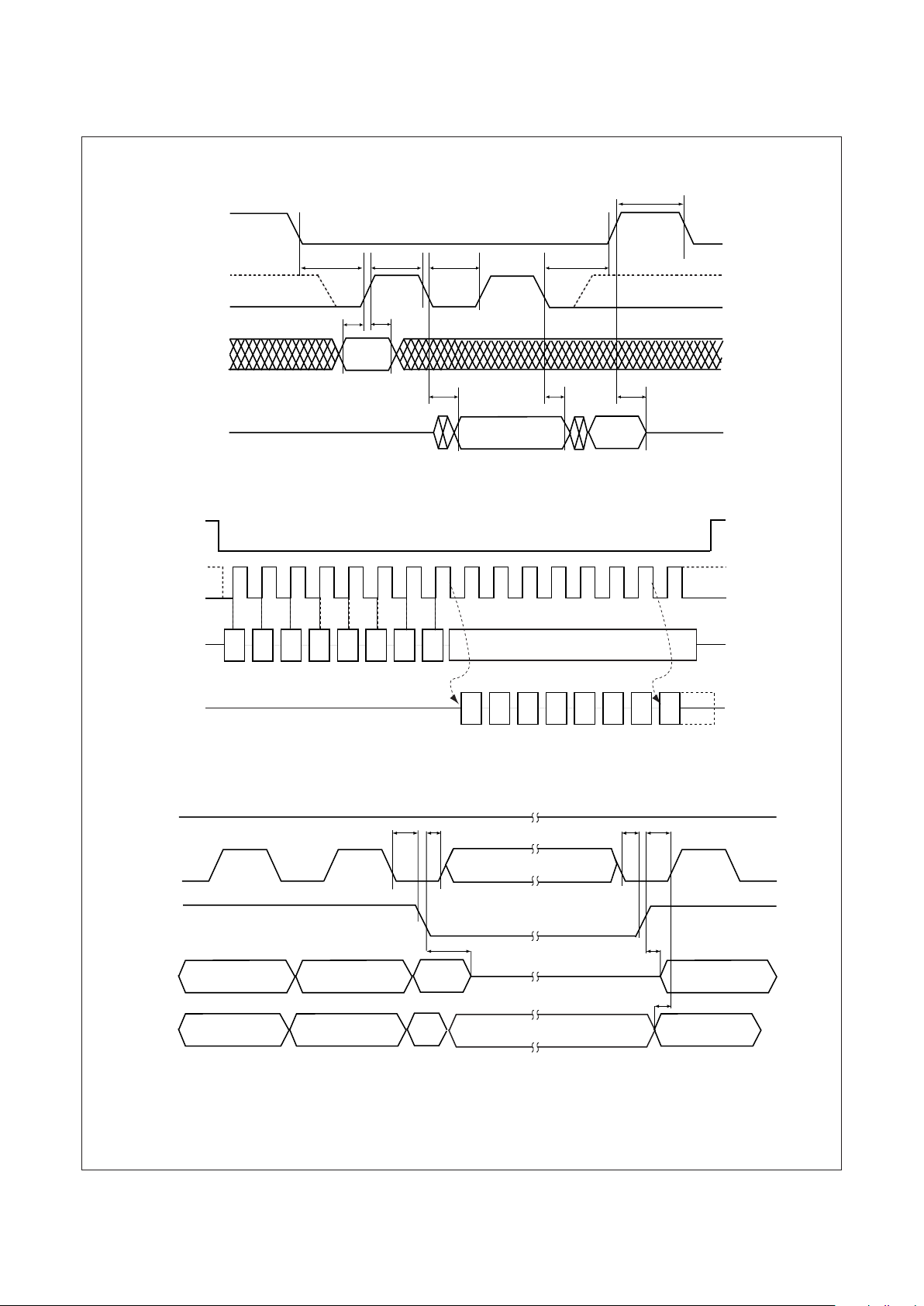
FIGURE 1. Synchronous Data Timing Diagram
t
CSS
t
CLH
t
CLL
t
CSH
t
DF
t
PD
t
DIStDIH
t
DH
t
CSI
SCK
SI
SO
/CS
Valid Input
Valid Output
High Z
Mode 3Mode 3
Mode 0Mode 0
SCK
CS
SO
/HOLD
Output (n+1) Output (n)Output (n)Output (n+2)
t
HDS
t
HZ
t
LZ
t
HDH
t
HDS
t
HDH
t
DIS
High Z
SI
Input (n+1) Input (n)Input (n)Input (n+2)
Don't Care
Low state ( /CS = 0)
Don't Care
FIGURE 3. HOLD Timing
FIGURE 2. SPI Protocol
SCK
SI
SO
/CS
Bit 7 Bit 6 Bit 5 Bit 4 Bit 3 Bit 2 Bit 1 Bit 0
Bit 7 Bit 6 Bit 5 Bit 4 Bit 3 Bit 2 Bit 1 Bit 0
Don't Care
High Z
Mode 3Mode 3
Page 6
6
www.fairchildsemi.com
FM25C640U Rev. B
FM25C640U 64K-Bit SPI Interface Serial CMOS EEPROM
Pin Description
Chip Select (/CS)
This is an active low input pin to the EEPROM and is generated by
a master that is controlling the EEPROM. A low level on this pin
selects the EEPROM and a high level deselects the EEPROM. All
serial communications with the EEPROM is enabled only when
this pin is held low.
Serial Clock (SCK)
This is an input pin to the EEPROM and is generated by the master
that is controlling the EEPROM. This is a clock signal that
synchronizes the communication between a master and the
EEPROM. All input information (SI) to the EEPROM is latched on
the rising edge of this clock input, while output data (SO) from the
EEPROM is driven after the falling edge of this clock input.
Serial Input (SI)
This is an input pin to the EEPROM and is generated by the master
that is controlling the EEPROM. The master transfers Input
information (Instruction Opcodes, Array addresses and Data)
serially via this pin into the EEPROM. This Input information is
latched on the rising edge of the SCK.
Serial Output (SO)
This is an output pin from the EEPROM and is used to transfer
Output data via this pin to the controlling master. Output data is
serially shifted out on this pin after the falling edge of the SCK.
Hold (/HOLD)
This is an active low input pin to the EEPROM and is generated by
the master that is controlling the EEPROM. When driven low, this
pin suspends any current communication with the EEPROM. The
suspended communication can be resumed by driving this pin
high. This feature eliminates the need to re-transmit the entire
sequence by allowing the master to resume the communication
from where it was left off. This pin should be tied high if this feature
is not used. Refer Hold Function description for additional
details.
Write Protect (/WP)
This is an active low input pin to the EEPROM. This pin allows
enabling and disabling of writes to memory array and status
register of the EEPROM. When this pin is held low, writes to the
memory array and status register are disabled. When this pin is
held high, writes to the memory array and status register are
enabled. Status of this pin does not affect operations other than
array write and status register write. /WP signal going low at any
time will inhibit programming, except when an internal write has
already begun. If an internal write cycle has already begun, /WP
signal going low will have no effect on the write. Refer Table1 for
Write Protection matrix.
Functional Description
The Serial Peripheral Interface (SPI) of FM25C640U consists of
an 8-bit Instruction register to decode a specific instruction to be
executed. Six different instructions (Opcodes) are incorporated
on FM25C640U for various operations. Table2 lists the instructions set and the format for proper operation. All Opcodes, Array
addresses and Data are transferred in “MSB first-LSB last”
fashion. Detailed information is provided under individual instruction descriptions.
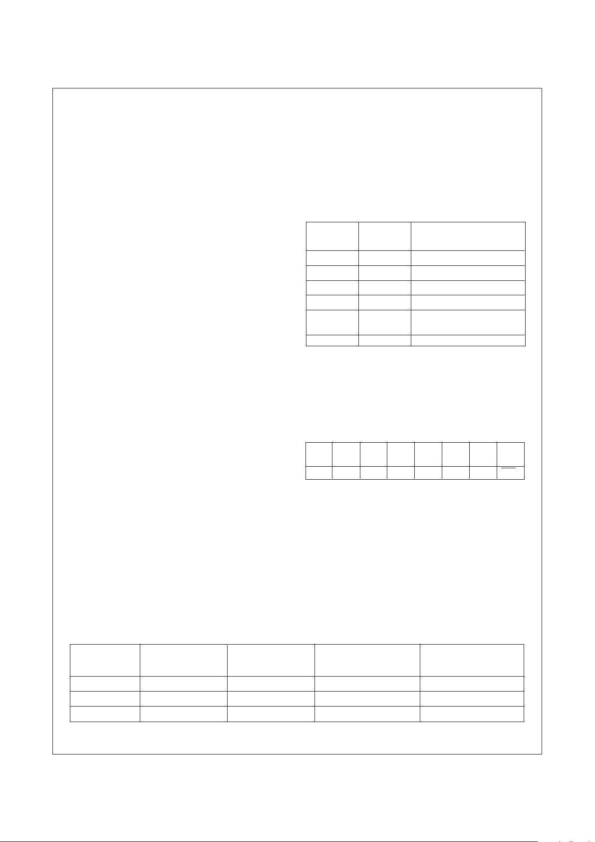
TABLE 2. Instruction Set
Instruction Instruction Operation
Name Opcode
WREN 00000110 Write Enabled
WRDI 00000100 Write Disabled
RDSR 00000101 Read Status Register
WRSR 00000001 Write Status Register
READ 00000011 Read Data from Memory
Array
WRITE 00000010 Write Data to Memory Array
In addition to the Instruction register, FM25C640U also contains
an 8-bit Status register that can be accessed by RDSR and WRSR
instructions. Only the least significant (LSB) 4 bits are defined at
present and the most significant (MSB) 4 bits are undefined (don’t
care). The LSB 4 bits define Block Write Protection levels (BP1and
BP0), Write-enable status (WEN) and Busy/Rdy status (/RDY) of
the EEPROM. Table 3 illustrates the format:
TABLE 3. Status Register Format
Bit Bit Bit Bit Bit Bit Bit Bit
76543210
X X X X BP1 BP0 WEN RDY
Refer RDSR and WRSR instruction descriptions for additional
information on Status register operations.
Table1. Write Protection Matrix
Protected Blocks
/WP Pin WEN Bit Status Register (by BP1-BP0) Unprotected Blocks
Low X Write Protected Write Protected Write Protected
High 0 Write Protected Write Protected Write Protected
High 1 Write Allowed Write Protected Write Allowed
Page 7
7
www.fairchildsemi.com
FM25C640U Rev. B
FM25C640U 64K-Bit SPI Interface Serial CMOS EEPROM
Functional Description (Continued)
SPI communication
As mentioned before, serial communication with the EEPROM is
enabled when the /CS pin is held low and the /HOLD pin is held
high. Input data (Instruction Opcodes, Array addresses and Data)
on the SI pin is latched in on the rising edges of SCK clock signal,
starting from the first rising edge after the /CS pin goes low. During
the time the SI data is input into the EEPROM, the SO pin remains
in high impedance state. If the intended instruction is of read
nature (Array read and Status register read), then data from the
EEPROM is driven out actively on the SO pin from every falling
edge of the SCK after the last input data (SI) is latched in. During
the time the SO data is output from the EEPROM, the data on the
SI pin is ignored.
Figure 2
illustrates the above. Refer
Figure 1
for
timing information.
HOLD function
An active communication with the EEPROM can be temporarily
suspended by bringing the /HOLD pin low when a EEPROM is
selected (/CS pin should be low) and a serial sequence with the
EEPROM is currently underway. To suspend the communication,
/HOLD pin must be driven low while SCK is low, otherwise the Hold
function will not be invoked until the next SCK high to low
transition. The EEPROM must remain selected during this sequence. Transitions on the SCK and SI pins are ignored during the
time the part is suspended and the SO pin will be in high
impedance state. Releasing the /HOLD pin back to high state will
allow the operation to resume from the point it was suspended.
/HOLD pin must be driven high while the SCK pin is low, otherwise
serial communication will not resume until the next SCK high to
low transition. Asserting a low on the /HOLD pin at any time will tristate the SO pin.
Figure 3
illustrates Hold timing.
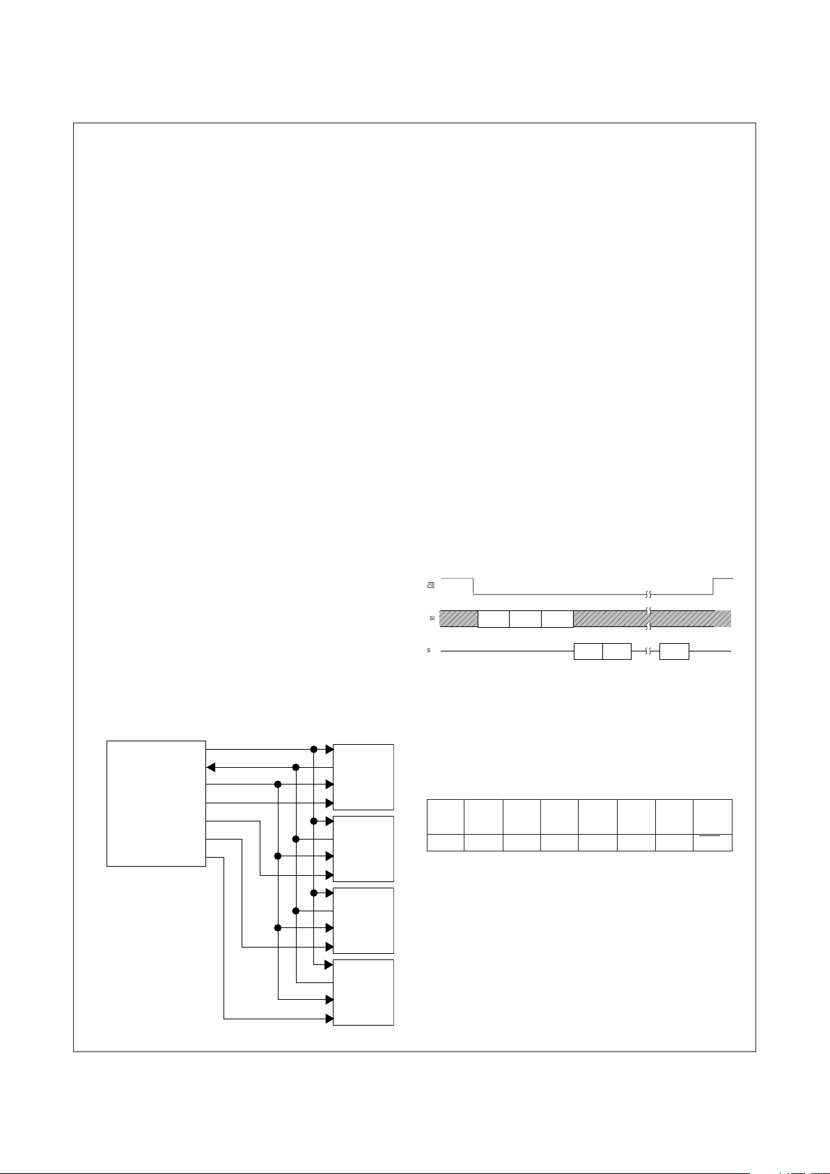
System Configuration
When multiple SPI peripherals (for e.g. EEPROMs) are present on
the bus, the SI, SO and the SCK signals can be tied together.
Figure
4 illustrates a typical system configuration with respect to
/CS, SCK, SI and SO pins.
FIGURE 4. System Configuration
SI
SO
SCK
/CS
DATA OUT (MOSI)
DATA IN (MISO)
SERIAL CLOCK (SPICK)
SS0
SS1
SS2
SS3
SI
SO
SCK
/CS
SI
SO
SCK
/CS
SI
SO
SCK
/CS
SELECTION
CHIP
SPI
MASTER MCU
FM25Cxxx
SPI Modes 0 and 3 (00 and 11)
FM25C640U supports both Mode 0 and Mode 3 of operations.
The difference between Mode 0 and Mode 3 is determined by the
state of the SCK clock signal when a SPI cycle starts (when /CS
is driven low) as well as when the SPI cycle ends (when /CS is
driven high). Under Mode 0 of operation, the SCK signal is held low
both at the start and at the end of a SPI cycle. Under Mode 1 of
operation, the SCK signal is held high both at the start and at the
end of a SPI cycle. However in both of these two modes, the input
data (SI) is sampled (latched in) at the rising edge of the SCK clock
signal and the output data (SO) is driven after the falling edge of
the SCK clock signal. See
Figure
1 and
Figure
2.
READ SEQUENCE (READ)
Reading the memory via the serial SPI link requires the following
sequence. The/CS pin is pulled low to select the EEPROM. The
READ opcode is transmitted on the SI pin followed by two bytes of
address, "High byte addr" (A15-A8) and "Low byte addr" (A7-A0).
After this is done, data on the SI pin becomes don't care. The data
(D7-D0) form the address specified is then shifted out on the SO pin.
If only one byte is to be read, the /CS pin can be pulled back to the
high level. It is possible to continue the READ sequence as the byte
address is automatically incremented and data will continue to be
shifted out as clock pulses are continuously applied. When the end
of memory array is reached (last byte location), the address counter
rolls over to the start of memory array (first byte location) allowing
the entire memory to be read in one continuous READ cycle. See
Figure 5. Note that only A12-A0 address bits are treated valid by
FM25C640U while bits A15-A13 are ignored.
FIGURE 5. Read Sequence
CS
SI
SO
Read
Opcode
High Byte
Addr
Low Byte
Addr
Data
(1)
Data
(2)
Data
(n)
READ STATUS REGISTER (RDSR):
The Read Status Register (RDSR) instruction provides read
access to the status register. As mentioned before, of the 8bits of
data, only the LSB 4bits are valid and they indicate Block Protection information (BP1 and BP0), Write Enable status (WEN) and
Busy/Ready status (/RDY) of the EEPROM. MSB 4bits of are
invalid (Don’t cares) Following is the format of RDSR data:
TABLE 3. Status Register Format
Bit Bit Bit Bit Bit Bit Bit Bit
76543210
X X X X BP1 BP0 WEN RDY
Bit3 (BP1) and Bit2 (BP0) together indicate Block write protection
previously set on the EEPROM. Refer Table 2.
Bit1 (WEN) indicates the Write enable status of the EEPROM.
This bit is a read-only bit and is read by executing RDSR
instruction. If this bit is “1” then the EEPROM is write enabled. If
this bit is “0” then the EEPROM is write disabled.
Page 8
8
www.fairchildsemi.com
FM25C640U Rev. B
FM25C640U 64K-Bit SPI Interface Serial CMOS EEPROM
Bit0 (/RDY) indicates the Busy/Ready status of the EEPROM.
This bit is a read-only bit and is read by executing RDSR
instruction. If this bit is “1” then the EEPROM is busy doing a
program cycle. If this bit is “0” then the EEPROM is ready.
Note that if a RDSR instruction is executed when an internal
programming cycle is in progress, only the /RDY bit is valid.
All other bits are don’t cares.
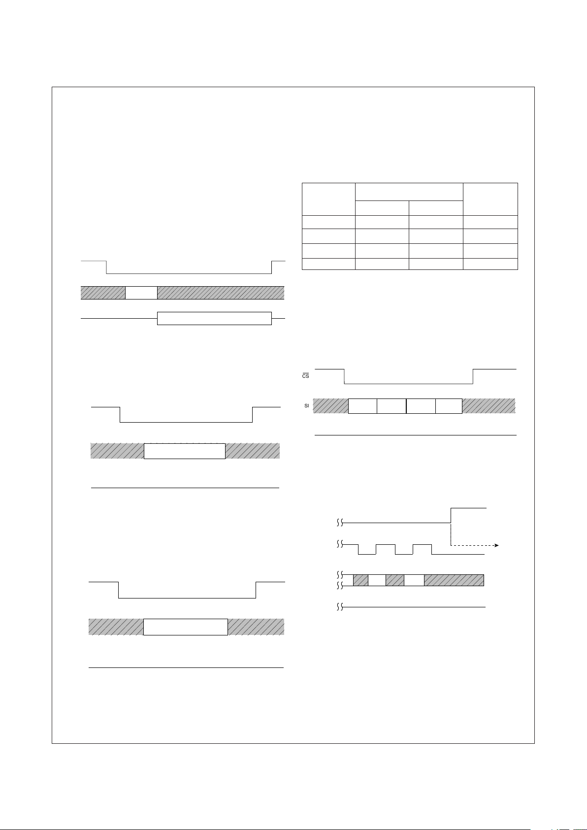
The RDSR command requires the following sequence. The /CS
pin is pulled low to select the EEPROM and then the RDSR
opcode is transmitted on the SI pin. After this is done, data on the
SI pin becomes don’t care. The data from the Status Register is
then shifted out on the SO pin starting with D7 bit first and D0 last.
See
Figure 6.
FIGURE 6. Read Status Register
WRITE SEQUENCE (WRITE):
Write to the array is enabled only when /WP pin is held high and
the EEPROM is write enabled previously (via WREN instruction).
Also, the address of the memory location(s) to be programmed
must be outside the protected address field selected by the Block
Write Protection Level. See Table 4.
TABLE 4. Block Write Protection Levels
Level Status Register Bits Array
Address
BP1 BP0 Protected
0 0 0 None
1 0 1 1800-1FFF
2 1 0 1000-1FFF
3 1 1 0000-1FFF
A WRITE command requires the following sequence. The /CS pin
is pulled llow to select the EEPROM, then the WRITE opcode is
transmitted on the SI pin followed by two bytes of address, "High
byte addr" (A15-A8) and "Low byte addr" (A7-A0), further followed
by the data (D7-D0) to be written. See Figure 9. Note that only A12A0 address bits are treated valid by FM25C640U while bits A15A13 are ignored.
FIGURE 9. Byte Write
/
CS
SI
SO
RDSR
OP-CODE
RDSR DATA
WRITE ENABLE (WREN):
When VCC is applied to the EEPROM, it “powers up” in a writedisabled state. Therefore, all programming modes (Write to memory
array and Status register), must be preceded by a WRITE ENABLE (WREN) instruction. See
Figure
7.
FIGURE 7. Write Enable
/CS
SI
SO
WREN Op-Code
WRITE DISABLE (WRDI):
Executing this instruction disables all programming modes (Write
to memory array and Status register), preventing the EEPROM
from accidental writes. Once WRDI instruction is executed,
WREN instruction should be executed to re-enable all programming modes. See
Figure
8.
FIGURE 8. Write Disable
/CS
SI
SO
WRDI Op-Code
CS
SI
SO
Write
Opcode
High Addr
Byte
Low Addr
Byte
Data
High Z
Internally, the programming will start after the /CS pin is brought
back to a high level. Note that the LOW to HIGH transition of the
/CS pin must occur during the SCK low time immediately after
clocking in the D0 data bit. See
Figure
10.
FIGURE 10. Start of Programming
SCK
SI
SO
/CS
D0D1D2
High Z
Start of internal
programming
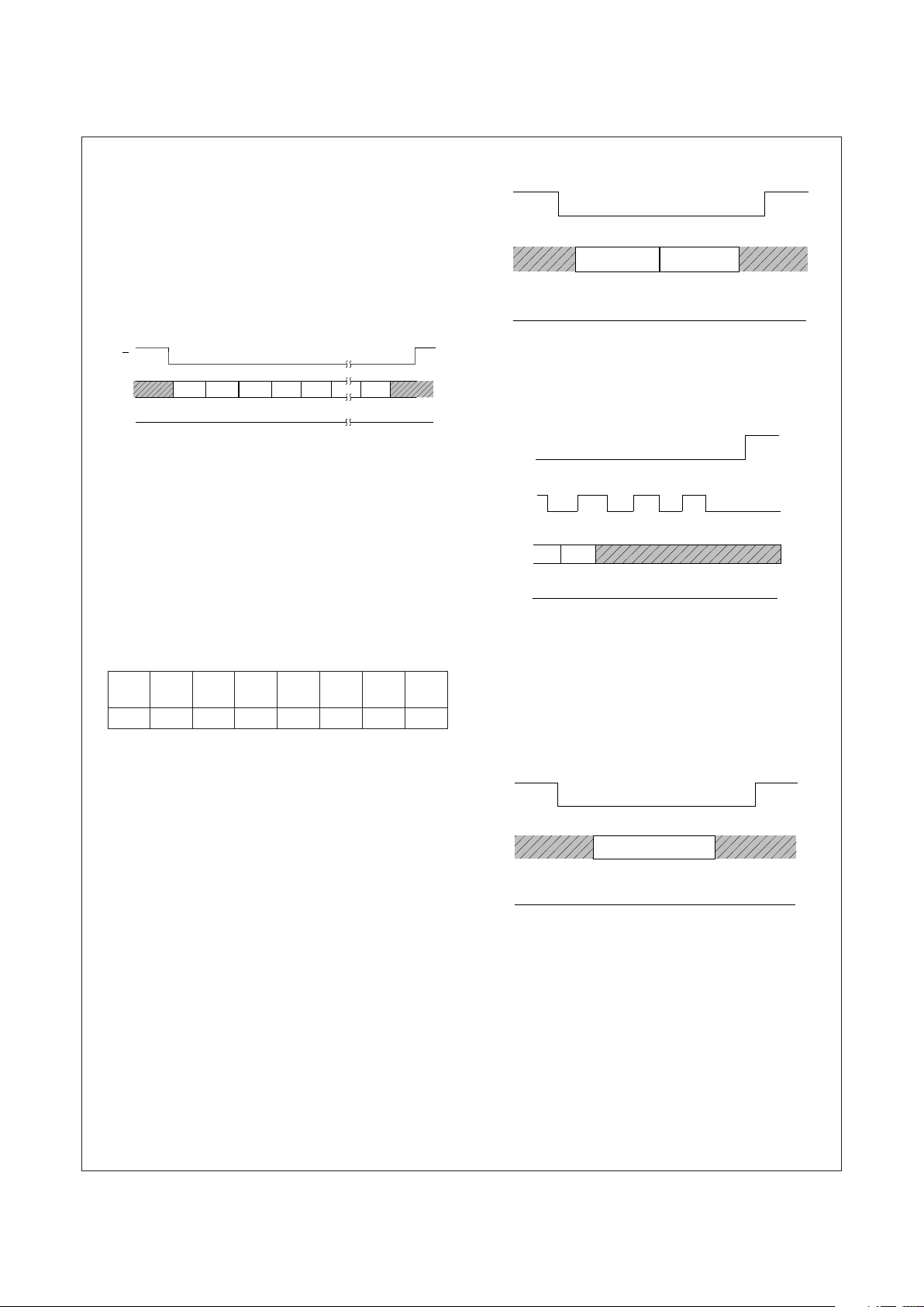
Programming status (Busy/Ready) of the EEPROM can be determined by executing a READ STATUS REGISTER (RDSR) instruction after a write command. Upon executing the RDSR
instruction, if Bit 0 of the RDSR data is “1”, it indicates the WRITE
cycle is still in progress. If it is “0” then the WRITE cycle has ended.
Note that while the internal programming is still in progress (Bit 0
= 1), only the RDSR instruction is enabled. It is recommended that
no other instruction be issued till the internal programming is
complete.
Page 9
9
www.fairchildsemi.com
FM25C640U Rev. B
FM25C640U 64K-Bit SPI Interface Serial CMOS EEPROM
The FM25C640U is also capable of a 32 byte PAGE WRITE
operation. Page write is performed similar to byte write operation
described above. During a Page write operation, after the first byte
of data, additional bytes (up to 31 bytes) can be input, before
bringing the /CS pin high to start the programming. After receipt of
each byte of data, the EEPROM internally increments the four low
order address bits (A4-A0) by one. The high order address bits
(A12-A5) will remain constant. If the master should transmit more
than 32 bytes of data, the address counter (A4-A0) will “roll over”
and the previously loaded data will be reloaded. See
Figure
11.
FIGURE 11. Page Write
CS
SI
SO
Write
Opcode
High Addr
Byte
Low Addr
Byte
Data
(1)
Data
(2)
Data
(32)
High Z
/CS
SI
SO
WRSR
Op-Code
SR Data
xxxxBP1BP0xx
FIGURE 12. Write Status Register
BP0
SCK
SI
SO
/CS
/CS
SI
SO
INVALID CODE
At the completion of a write cycle the EEPROM is automatically
returned to the write disabled state. Note that if the EEPROM is not
write enabled (WEN=0) before issuing the WRITE instruction, the
EEPROM will ignore the WRITE instruction and return to the
standby state when /CS is brought high.
WRITE STATUS REGISTER (WRSR):
The Write Status Register (WRSR) instruction provides write
access to the status register. This instruction is used to set Block
Write protection to a portion of the array as defined under Table
4. During a WRSR instruction only Bit3 (BP1) and Bit2 (BP0) can
be written with valid information while other bits are ignored.
Following is the format of WRSR data:
Status Register Write Data
Bit Bit Bit Bit Bit Bit Bit Bit
76543210
X X X X BP1 BP0 X X
X = Don’t Care
Note that the first four bits are don’t care bits followed by BP1 and
BP0 and two more don’t care bits.
WRSR instruction is enabled only when /WP pin is held high and
the EEPROM is write enabled previously (via WREN instruction).
WRSR command requires the following sequence. The /CS pin is
pulled low to select the EEPROM and then the WRSR opcode is
transmitted on the SI pin followed by the data to be programmed.
See
Figure 12.
Programming will start after the /CS pin is forced back to a high
level. As in the WRITE instruction the LOW to HIGH transition of
the /CS pin must occur during the SCK low time immediately after
clocking in the last don’t care bit. See
Figure 13.
FIGURE 13. Start WRSR Condition
At the completion of this instruction the EEPROM is automatically
returned to write disabled state.
INVALID OPCODE
If an invalid code is received, then no data is shifted into the
EEPROM, and the SO data output pin remains high impedance
state until a new /CS falling edge reinitializes the serial communication. See
Figure
14.
FIGURE 14. Invalid Op-Code
Page 10
10
www.fairchildsemi.com
FM25C640U Rev. B
FM25C640U 64K-Bit SPI Interface Serial CMOS EEPROM
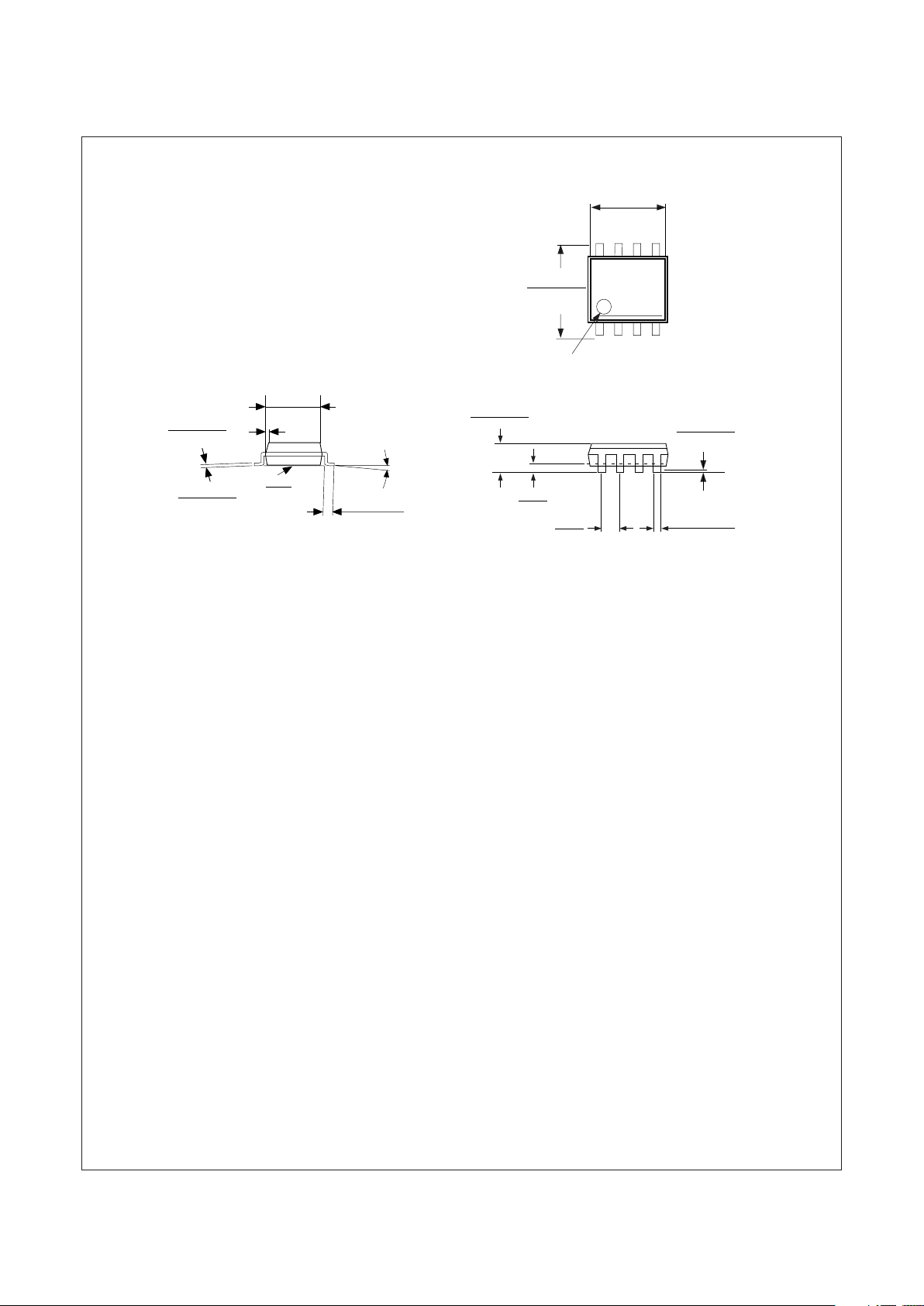
Molded Small Out-Line Package (M8)
Package Number M08A
1234
8765
0.189 - 0.197
(4.800 - 5.004)
0.228 - 0.244
(5.791 - 6.198)
Lead #1
IDENT
Seating
Plane
0.004 - 0.010
(0.102 - 0.254)
0.014 - 0.020
(0.356 - 0.508)
0.014
(0.356)
Typ.
0.053 - 0.069
(1.346 - 1.753)
0.050
(1.270)
Typ
0.016 - 0.050
(0.406 - 1.270)
Typ. All Leads
8° Max, Typ.
All leads
0.150 - 0.157
(3.810 - 3.988)
0.0075 - 0.0098
(0.190 - 0.249)
Typ. All Leads
0.004
(0.102)
All lead tips
0.010 - 0.020
(0.254 - 0.508)
x 45°
Physical Dimensions inches (millimeters) unless otherwise noted
Page 11
11
www.fairchildsemi.com
FM25C640U Rev. B
FM25C640U 64K-Bit SPI Interface Serial CMOS EEPROM
Physical Dimensions inches (millimeters) unless otherwise noted
Life Support Policy
Fairchild's products are not authorized for use as critical components in life support devices or systems without the express written
approval of the President of Fairchild Semiconductor Corporation. As used herein:
1. Life support devices or systems are devices or systems which,
(a) are intended for surgical implant into the body, or (b) support
or sustain life, and whose failure to perform, when properly
used in accordance with instructions for use provided in the
labeling, can be reasonably expected to result in a significant
injury to the user.
2. A critical component is any component of a life support device
or system whose failure to perform can be reasonably expected to cause the failure of the life support device or system,
or to affect its safety or effectiveness.
Fairchild Semiconductor Fairchild Semiconductor Fairchild Semiconductor Fairchild Semiconductor
Americas Europe Hong Kong Japan Ltd.
Customer Response Center Fax: +44 (0) 1793-856858 8/F, Room 808, Empire Centre 4F, Natsume Bldg.
Tel. 1-888-522-5372 Deutsch Tel: +49 (0) 8141-6102-0 68 Mody Road, Tsimshatsui East 2-18-6, Yushima, Bunkyo-ku
English Tel: +44 (0) 1793-856856 Kowloon. Hong Kong Tokyo, 113-0034 Japan
Français Tel: +33 (0) 1-6930-3696 Tel; +852-2722-8338 Tel: 81-3-3818-8840
Italiano Tel: +39 (0) 2-249111-1 Fax: +852-2722-8383 Fax: 81-3-3818-8841
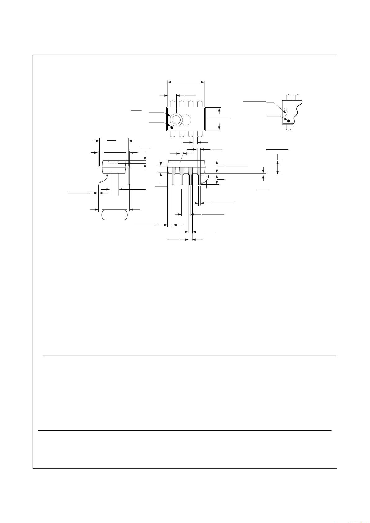
Molded Dual-In-Line Package (N)
Package Number N08E
0.373 - 0.400
(9.474 - 10.16)
0.092
(2.337)
DIA
+
1234
8765
0.250 - 0.005
(6.35 ± 0.127)
87
0.032 ± 0.005
(0.813 ± 0.127)
Pin #1
Option 2
RAD
1
0.145 - 0.200
(3.683 - 5.080)
0.130 ± 0.005
(3.302 ± 0.127)
0.125 - 0.140
(3.175 - 3.556)
0.020
(0.508)
Min
0.018 ± 0.003
(0.457 ± 0.076)
90° ± 4°
Typ
0.100 ± 0.010
(2.540 ± 0.254)
0.040
(1.016)
0.039
(0.991)
Typ.
20° ± 1°
0.065
(1.651)
0.050
(1.270)
0.060
(1.524)
Pin #1 IDENT
Option 1
0.280
MIN
0.300 - 0.320
(7.62 - 8.128)
0.030
(0.762)
MAX
0.125
(3.175)
DIA
NOM
0.009 - 0.015
(0.229 - 0.381)
0.045 ± 0.015
(1.143 ± 0.381)
0.325
+0.040
-0.015
8.255
+1.016
-0.381
95° ± 5°
0.090
(2.286)
(7.112)
IDENT
 Loading...