

Page 1
www.fairchildsemi.com
FM20
Ultra-Low-Power Analog Temperature Sensor
Features
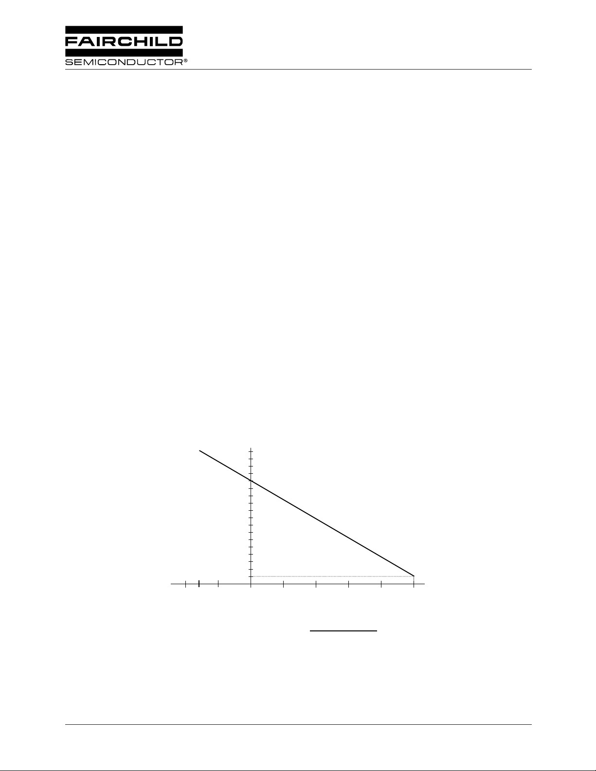
• Analog Output, -11.77mV/°C
• Range, -55 to 130°C
• Accuracy, ±1°C at 25°C
• Supply Current, 9µA typical
• Output Drive, 1µA
• Self-heating < 0.021°C
• Operating Voltage: +2.4V to +6V
Applications
• Mobile Phones
• Computers
• Battery Management
• Office Equipment
•HVAC
• Power Supply Modules
• Disk Drives
• Automotive
Thermal Response
Description
As a precision CMOS temperature sensor, the FM20 is
cost-effective for accurate low-power temperature
monitoring applications. Output voltage versus temperature
is extremely linear. With no load, the supply current is
typically 1µA. For normal operation, the load on V
should be 5M Ω or less.
In a typical application, a remotely mounted FM20 is
monitored by a microcontroller with an analog A/D
converter input. Alternatively, the FM20 can drive a
comparator with a high impedance input.
Accuracy is typically ±1°C at room temperature; and better
than ±2.5°C from 0 to 50°C.
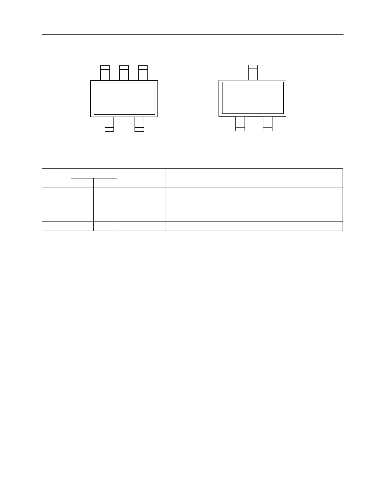
Available packages are surface mount 5-pin SC70 and 3-pin
SOT-23.
V
(mV)
OUT
OUT
1863.9
391
25 50 75 100 125-25-50 -40 0
Temperature (˚C)
V
– 1863.9mV
Temperature (˚C) =
FM20 Output Voltage vs. Temperature
OUT
–11.77mV/˚C
REV. 1.0.6 1/9/03
Page 2
FM20 PRODUCT SPECIFICATION
Pin Assignments
VOUT
GND
321
FM20
DD GND
V
Pin Descriptions
Pin No.
Pin Name
V
OUT
V
DD
GND 2, 5 3 Power
3 2 Analog Output Temperature Sense. Analog output voltage indicating
41 Power Supply Voltage. 2.4 to 6.0V
Type FunctionSC-70 SOT-23
N/C
54
temperature.
V
= 1863.9 – 11.77 T(°C) mV
OUT
Ground.
GND
3
FM20
12
VDD
VOUT
2
REV. 1.0.6 1/9/03
Page 3
≤
≤
PRODUCT SPECIFICATION FM20
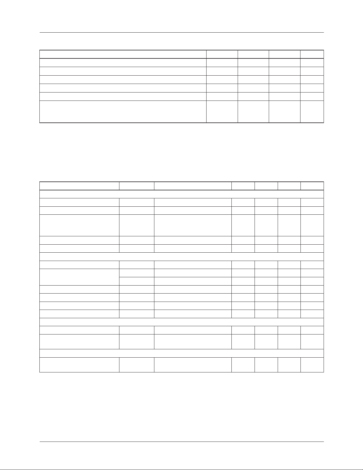
Absolute Maximum Ratings
1
Parameter Min. Typ. Max. Units
Supply Voltage +7 V
Output Voltage V
+ 0.5 V
DD
Output Current -20/+1 µA
Storage Temperature Range -60 +150 °C
Lead Soldering Temperature 220 °C
2
ESD
Human Body Model
Machine Model
Notes:
1. Absolute maximum ratings are limits beyond which operation may cause permanent damage to the device. These are stress
ratings only; functional operation at or above these limits is not implied.
2. Human Body Model: 100pF capacitor discharged through a 1.5k Ω resistor into each pin. Machine Model: 200pF capacitor
discharged directly into each pin.
Electrical Characteristics
Limits apply for -55°C ≤ T
+130°C and V
A
3
= +5.0V unless otherwise noted.
DD
2000
250
V
V
Parameter Symbol Conditions Min Typ Max Units
Transfer Characteristic
Sensitivity -11.77 mV/°C
Output at 0°C 1863.9 mV
Accuracy
4
T
= +25°C
A
T
= -55°C (T
A
T
= +130°C (T
A
MIN
)
MAX
-2
-3
)
-5
±1
±2
±2
+2
+3
+5
°C
°C
°C
Temperature Range -55 +130 °C
Non-Linearity
5
-0.5 +0.2 °C
Output
Output Voltage Range V
Output Current Source
Output Current Sink
6
6
I
ONSN
I
ONSG
I
OL
Output resistance T
OUT
< V
DD
300 2550 mV
Sensing 1 µA
Surge mA
20 µA
= 25°C k Ω
A
Load regulation mV/mA
Capacitive Load
7
C
L
100 1000 pF
Power
Supply Voltage V
Quiescent Supply Current
Output Floating
I
DD
DD
T
= +25°C
A
-55°C ≤ T
A
+130°C
2.4 6.0 V
9
9
11.5
14
µA
µA
Package
Self Heating SOT-23
SC70
0.02016
0.02082°C°C
Notes:
3. These specifications are guaranteed only for the test conditions listed.
4. Accuracy (expressed in °C) = Difference between calculated output voltage and measured output voltage. Calculated output
voltage = -11.77mV/°C multiplied by device’s case temperature at specified conditions of temperature, voltage and power
supply plus an offset of 1863.9 mV at 0°C.
5. Non-linearity is defined as the deviation of the output-voltage-versus-temperature curve from the best-fit straight line, over the
device's rated temperature range.
6. Lowest output current should be targeted; higher currents result in more self-heating of the device.
7. High capacitive loads may be driven by the output in a static mode, but it may require a delay time before initial read at power
up to allow for the RC time constant of the charging capacitor.
REV. 1.0.6 1/9/03
3
Page 4
FM20 PRODUCT SPECIFICATION
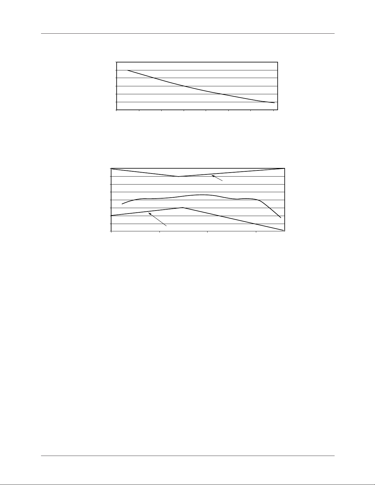
Typical Performance Characteristics
12
11
10
9
8
7
6
Quiescent Current (µA)
-50 -25 0 25 50 75 100 125
Temperature (°C)
Figure 1. Quiescent Current vs. Temperature
3
2
1
0
-1
-2
Accuracy (°C)
-3
-4
-5
-50 0 50 100
lower spec limit
upper spec limit
V
= +5V
DD
V
DD
=+5V
Temperature (°C)
Figure 2. Accuracy vs. Temperature
Applications Information
Mounting
The FM20 can be easily mounted by gluing or cementing it
to a surface. In this case, its temperature will be within about
0.2°C of the temperature of the surface it is attached to if the
ambient air temperature is almost the same as the surface
temperature. If the air temperature is much higher or lower
than the surface temperature, the actual temperature of the
FM20 die will be at an intermediate temperature between the
surface temperature and the air temperature.
To ensure good thermal conductivity, the backside of the
FM20 die is directly attached to the GND pin. The lands and
traces to the FM20 will, of course, be part of the printed
circuit board, which is the object whose temperature is being
measured. These printed circuit board lands and traces will
not cause the FM20’s temperature to deviate from the desired
temperature.
Alternatively, the FM20 can be mounted inside a sealed-end
metal tube, and can then be dipped into a bath or screwed
into a threaded hole in a tank. As with any IC, the FM20 and
accompanying wiring and circuits must be kept insulated and
dry to avoid leakage and corrosion. This is especially true if
the circuit may operate at cold temperatures where condensation can occur. Printed-circuit coatings and varnishes such as
Humiseal and epoxy paint or dips can be used to ensure that
moisture cannot corrode the FM20 or its connections.
Loading
The FM20 will handle sizable capacitive loads up to 300pF
without any special considerations. In an extremely noisy
environment it may be advisable to add some filtering to
minimize noise in the output voltage. It is also recommended
that a 0.1µF bypass capacitor be added between the supply
voltage and ground. This is due to the instant current demand
caused by switching CMOS transistors. Normally it is unadvisable to put a sufficiently large supply (particularly in
portable electronics) to be able to handle the dynamic currents of CMOS transistors. It is a much simpler solution to
use a bypass capacitor to sustain the supply voltage during
this short demand period.
4
REV. 1.0.6 1/9/03
Page 5
5
PRODUCT SPECIFICATION FM20
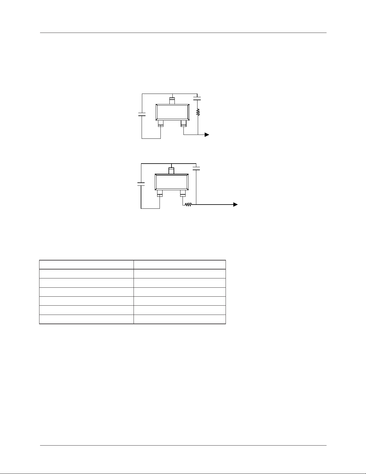
In environments that are particularly noisy it may be necessary to add a low-pass filter network to the output of the
device. As shown below, a 1µF capacitor in addition to the
output impedance of the device and a 200 Ω series resistor
for a low-pass filter that will pass the slow thermal time con-
GND
0.1µF
Bypass
Cap
V
0.1µF
Bypass
Cap
DD
V
DD
V
GND
V
stant of the FM20, while filtering the higher frequency noise.
The response time of the FM20 can be affected by this filter
network, therefore values for C
< 1500pF are recom-
FILTER
mended.
C
FILTER
R
FILTER
OUT
OUT
R
FILTER
C
FILTER
C
L
C
L
Figure 3. FM20 with Filter Network for Noisy Environments or for Capacitive Loads Greater than 300pF
Table 1. Resistor/Capacitor Combinations for Filter Network
R
FILTER
200 Ω
470 Ω
680 Ω
1000 Ω
10k Ω
100k Ω
C
FILTER
1µF
0.1µF
0.01µF
1000pF
100pF
10pF
REV. 1.0.6 1/9/03
Page 6
FM20 PRODUCT SPECIFICATION
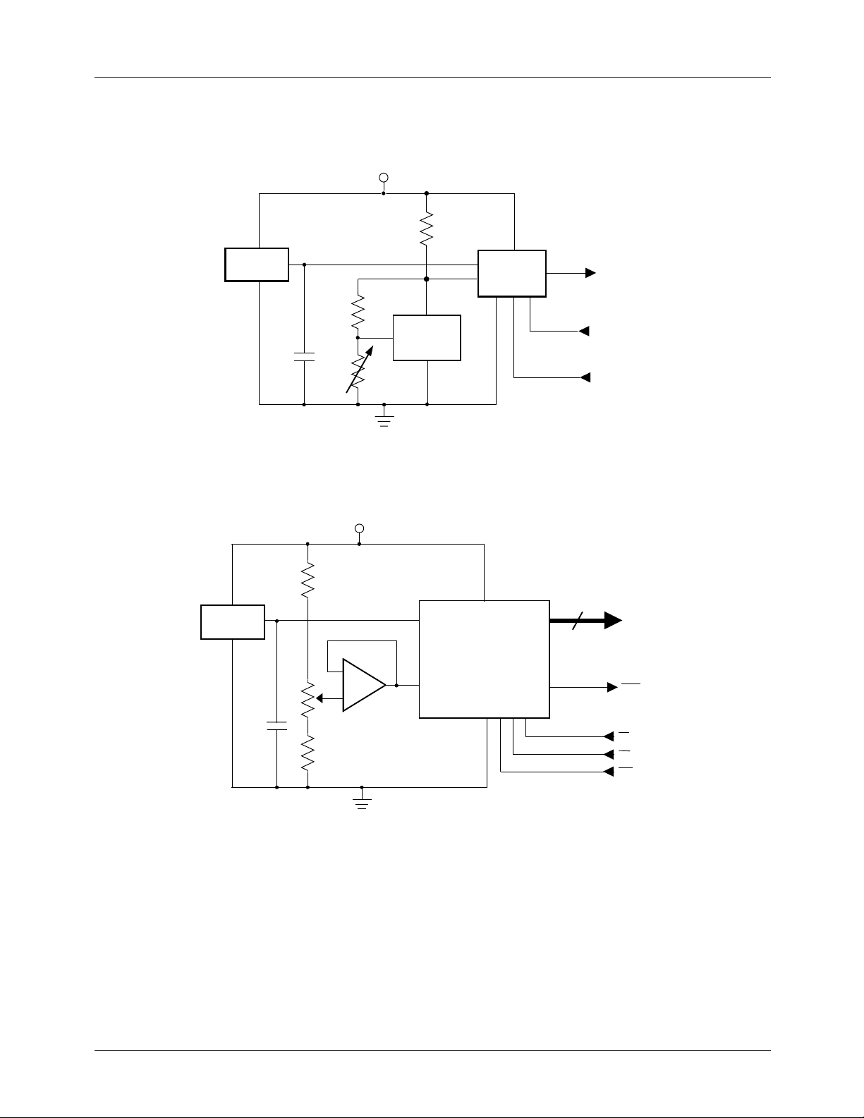
Example Applications Circuits
Typical Applications
5V
3.9KΩ
FM20
1µF
V
Temp
100KΩ
10KΩ
FB
Adjustable
Shunt Voltage
Reference
IN
Serial
Analog-to-Digital
REF
Converter
1.75V
+
SERIAL
DATA OUT
CLOCK
ENABLE
(The full scale of the A-to-D Converter will typically be limited to +125°C simply by the
Figure 4. Serial Output Temperature to Digital Converter
number of bits available in the conversion. The FM20 would still be capable of its full output swing.)
5V
30KΩ
FM20
V
Temp
IN
8
PARALLEL
DATA
OUTPUT
Parallel Output
Analog-to-Digital
Converter
V
REF
INTR
CS
RD
WR
1µF
5KΩ
15KΩ
_
+
1.75V
Figure 5. Parallel Output Temperature to Digital Converter (Full Scale = +125°C)
6
REV. 1.0.6 1/9/03
Page 7
PRODUCT SPECIFICATION FM20
Typical Applications (continued)
R
Shunt
Voltage Reference
V+
V+
V+
R
HYST
R
0.1µF
VD1
R
VD2
V
OUT
V
HYST2
V
HYST1
V
OUT
V
CONTROL
V
TRIP
V
CONTROL
) • (R
V
V
HYST2
HYST1
=
=
(V
REF
+
R
VD1
(V
REF
R
+
VD2
) • (R
(R
VD2
R
HYST
) • (R
(R
VD1
R
HYST + RVD1
VD2
+ R
VD2
) • (R
)
)
HYST
VD2
HYST
)
)
V
REF
FM20
V
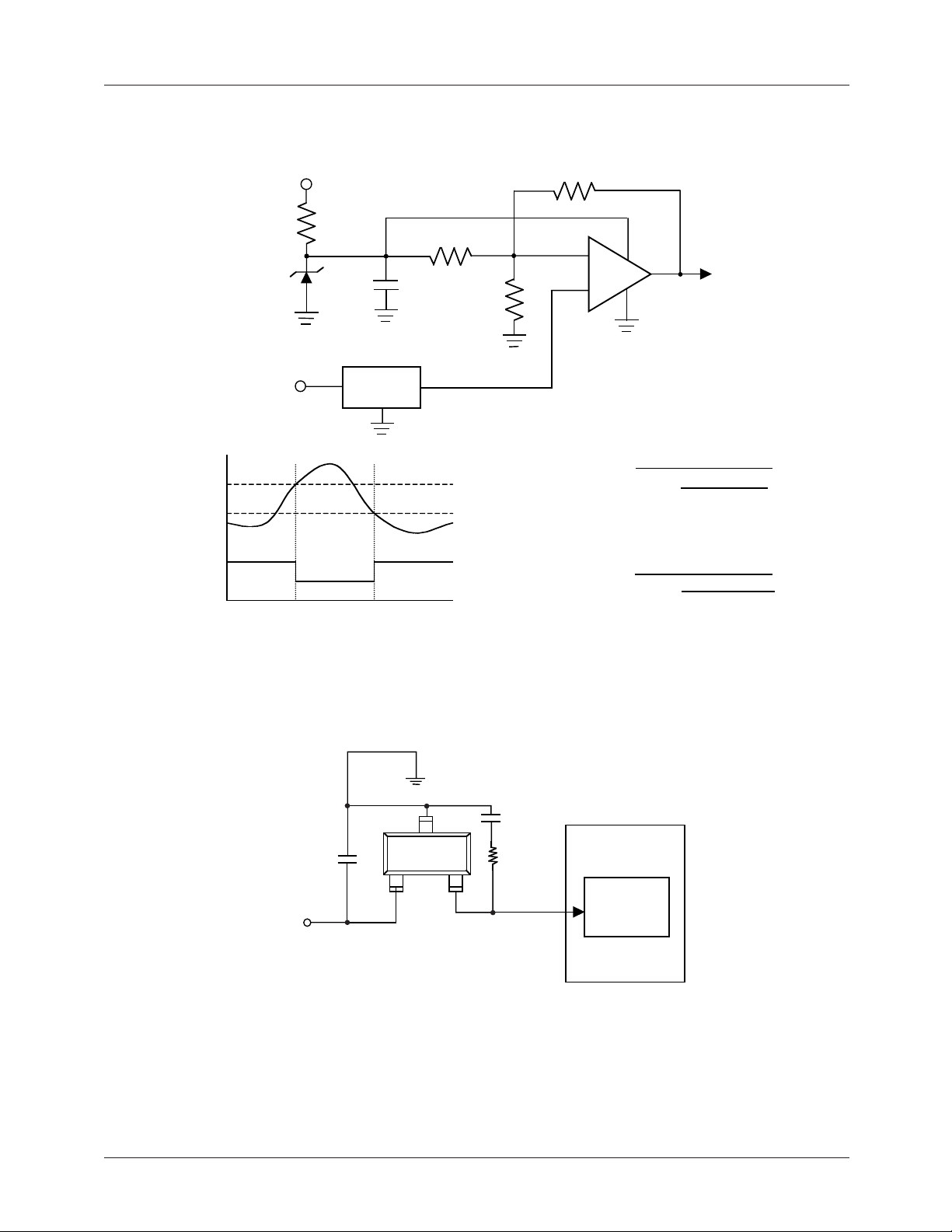
is set by the Shunt Voltage Reference. V
REF
state or control for activating cooling/fan.
high is an alarm
CONTROL
Figure 6. Thermostat/Fan Controller
GND
C
0.1µF
Bypass
FM20
FILTER
R
FILTER
Microcontroller
Cap
V
OUT
V
DD
Analog
to
Digital
Converter
Figure 7. Digital Temperature Output Through a Microcontroller
REV. 1.0.6 1/9/03
7
Page 8
FM20 PRODUCT SPECIFICATION
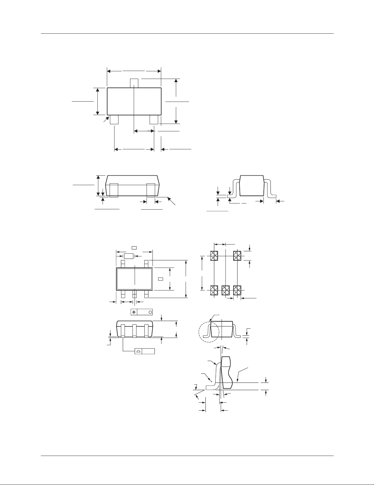
Mechanical Dimensions
inches (millimeters) unless otherwise noted
SOT-23 FS Package Code MA03A
0.110 (2.800)
0.120 (3.040)
0.047 (1.20)
0.055 (1.40)
PIN 1
0.070 (1.780)
0.081 (2.050)
0.035 (0.890)
0.044 (1.120)
0.0005 (0.013)
0.004 (0.100)
0.035 (0.890)
0.041 (1.030)
0.015 (0.370)
0.020 (0.510)
0.083 (2.100)
0.104 (2.640)
0.017 (0.450)
0.024 (0.600)
SEATING
PLANE
0.015 (0.085)
0.007 (0.180)
10°
0°
0.0217 REF (0.55) REF
SC70 5-pin FS Package Code MAA05A
-A-
2.00±0.20
0.65
54
321
+0.10
max 0.1
0.20
M
max 0.1
0.25
0.10
0.00
NOTES:
A. CONFORMS TO EIAJ REGISTERED OUTLINE DRAWING SC88A.
B. DIMENSIONS DO NOT INCLUDE BURRS OR MOLD FLASH.
C. DIMENSIONS ARE IN MILLIMETERS.
-0.05
0.9±.10
1.25±0.10
-B-
2.10±0.10
0.95±.15
1.9
LAND PATTERN RECOMMENDATION
SEE DETAIL A
R0.14
R0.10
0°-30°
6.00°
0.45
0.10
DETAIL A
0.65
.5 min
6.00°
GAGE PLANE
0.425 NOMINAL
0.25
0.10
0.4 min
0.20
8
REV. 1.0.6 1/9/03
Page 9

FM20 PRODUCT SPECIFICATION
Ordering Information
Part Number Package Temperature Range Shipping
FM20P5X 5-Pin SC70 -55°C to +130°C Tape and Reel, 3000 units/reel
FM20S3X 3-Pin SOT-23 -55°C to +130°C Tape and Reel, 3000 units/reel
DISCLAIMER
FAIRCHILD SEMICONDUCTOR RESERVES THE RIGHT TO MAKE CHANGES WITHOUT FURTHER NOTICE TO
ANY PRODUCTS HEREIN TO IMPROVE RELIABILITY, FUNCTION OR DESIGN. FAIRCHILD DOES NOT ASSUME
ANY LIABILITY ARISING OUT OF THE APPLICATION OR USE OF ANY PRODUCT OR CIRCUIT DESCRIBED HEREIN;
NEITHER DOES IT CONVEY ANY LICENSE UNDER ITS PATENT RIGHTS, NOR THE RIGHTS OF OTHERS.
LIFE SUPPORT POLICY
FAIRCHILD’S PRODUCTS ARE NOT AUTHORIZED FOR USE AS CRITICAL COMPONENTS IN LIFE SUPPORT DEVICES
OR SYSTEMS WITHOUT THE EXPRESS WRITTEN APPROVAL OF THE PRESIDENT OF FAIRCHILD SEMICONDUCTOR
CORPORATION. As used herein:
1. Life support devices or systems are devices or systems
which, (a) are intended for surgical implant into the body,
or (b) support or sustain life, and (c) whose failure to
perform when properly used in accordance with
2. A critical component in any component of a life support
device or system whose failure to perform can be
reasonably expected to cause the failure of the life support
device or system, or to affect its safety or effectiveness.
instructions for use provided in the labeling, can be
reasonably expected to result in a significant injury of the
user.
www.fairchildsemi.com
1/9/03 0.0m 003
2002 Fairchild Semiconductor Corporation
Stock#DS30000020
 Loading...