

Page 1
1/9
N-Channel MOS FET
FKP280A September, 2005
■Features
●Low on-resistance
●Low input capacitance
●Avalanche energy capability guaranteed
■Applications
●PDP driving
●High speed switching
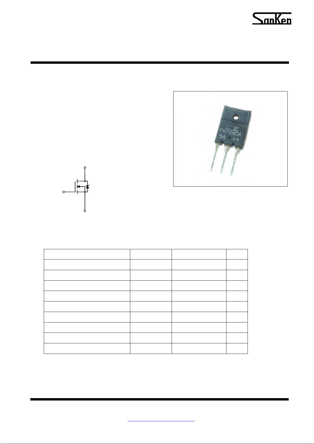
■Equivalent circuit
G(1)
D(2)
S(3)
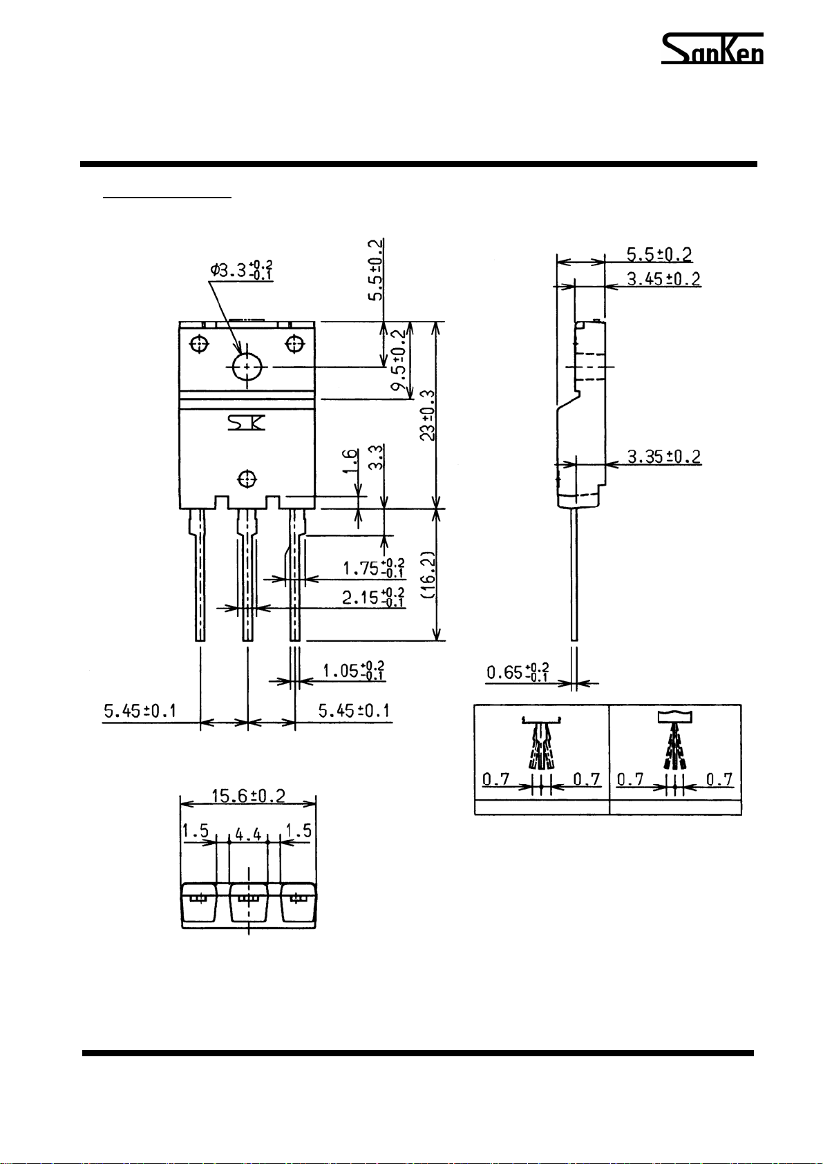
■Package---FM100(TO3P Full Mold)
■Absolute maximum ratings
(Ta=25°C)
Parameter Symbol Rating Unit
Drain to Source Voltage VDSS 280 V
Gate to Source Voltage VGSS ±30 V
Continuous Drain Current ID ±40A A
Pulsed Drain Current ID(pulse)
Maximum Power Dissipation PD 85 (Tc=25°C) W
Single Pulse Avalanche Energy EAS
Avalanche Current IAS 40 A
Channel Temperature Tch 150 °C
Storage Temperature Tstg -55 to +1 50 °C
*1. PW ≤ 100 μsec, duty cycle ≤ 1%
*2. VDD=20V, L=460μH, ILp=40A, unclamped, RG=50Ω, See Fig.1
*1
±160A A
*2
400 mJ
Sanken Electric Co.,Ltd.
http://www.sanken-ele.co.jp/en/
T02-001EA-050912
Page 2
2/9
N-Channel MOS FET
FKP280A September, 2005
Electrical characteristics
(Ta=25°C)
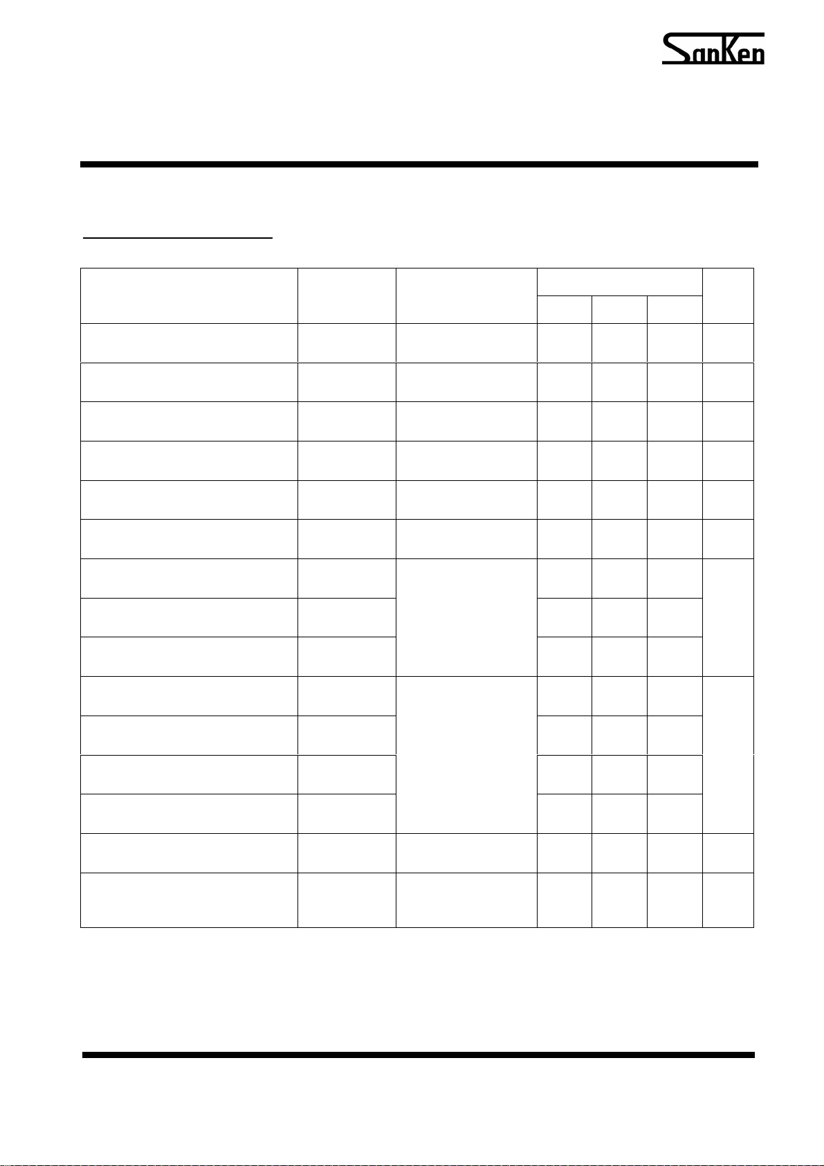
Parameter Symbol Test Conditions
Drain to Source breakdown Voltage
Gate to Source Leakage Current
Drain to Source Leakage Current
Gate Threshold Voltage
Forward Transconductance
Static Drain to Source On-Resistance
Input Capacitance
Output Capacitance
Reverse Transfer Capacitance
Limits
MIN. TYP. MAX.
V(BR)DSS ID=100μA,VGS=0V 280 V
IGSS VGS=±30V ±100 nA
IDSS V
VTH VDS=10V, ID=1mA
Re(Yfs) VDS=10V, ID=20A 25 38 S
RDS(ON) I
Ciss 3800
Coss 580
Crss
DS=280V, VGS=0V 100 μA
3.0
D=20A, VGS=10V 46 53 mΩ
V
DS=25V
GS=0V
V
f=1MHz
190
4.5
Unit
V
pF
Turn-On Delay Time
Rise Time
Turn-Off Delay Time
Fall Time
Source-Drain Diode Forward Voltage
Gate Threshold Voltage Te mp.
Coefficient
td(on)
tr
td(off)
tf
VSD ISD=40A,VGS=0V 1.0 1.5 V
ΔVTH/ΔTch
D=20A, VDD≈140V
I
RL=7Ω, VGS=10V
Rg=5Ω
See Fig.2
VDS=10V, ID=1mA -11 mV/°C
40
90
160
70
Sanken Electric Co.,Ltd.
ns
T02-001EA-050912
Page 3
3/9
N-Channel MOS FET
FKP280A September, 2005
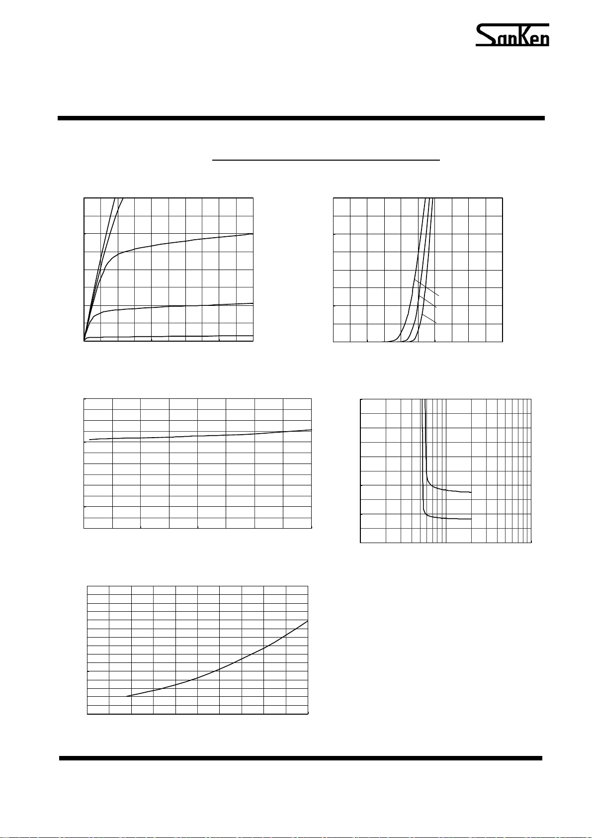
Characteristic Curves (Tc=25°C)
40
30
ID-VDS Characteristics (typical)
VGS=1 0V
6.0V
5.5V
20
ID (A)
10
5.0V
0
0246810
VDS (V)
4.5V
60
50
40
30
RDS(on) (mΩ)
20
RDS(ON)-ID Cha racteristics (typical)
VGS=10V
10
0
0 10203040
150
RDS(ON)-Tc Characteristics (typical)
ID (A)
ID=20A
VGS=10V
ID-VGS Characteristics (typical)
40
30
20
ID (A)
10
0
0246810
5
4
3
VDS (V)
2
1
0
1 10 100
VGS ( V)
VDS-VGS Characteristics (typical)
125℃
25℃
Tc=-55℃
VGS ( V)
VDS=10V
ID=40A
20A
100
RDS(on) (mΩ)
50
0
-100 -50 0 50 100 150
Tc (℃)
Sanken Electric Co.,Ltd.
T02-001EA-050912
Page 4

4/9
N-Channel MOS FET
FKP280A September, 2005
Characteristic Curves (Tc=25°C)
Re(yfs)-ID Characteristics (typical)
100
10
1
Re(yfs) (S)
0.1
Tc=-55℃
25℃
125℃
0.01
0.01 0.1 1 10 100
40
IDR-VSD Characteristics (typical)
ID (A)
30
20
ID (A )
10V
10
VGS=0V
0
0.0 0.5 1.0 1.5
100
PD-Ta Characteristics
VSD (V)
80
VDS=10V
Capacitance-VDS Characteristics (typical)
10000
1000
Capacitance (pF)
100
10
0 1020304050
SAFE OPERATI NG AREA
1000
ID(pu lse) max
100
ID max
10
ID (A)
1
0.1
0.01
0.1 1 10 100 1000
RDS(on) LIMITED
Tc=25℃
1sh ot
VDS (V)
VDS (V)
f=1MHz
VGS=0V
Ciss
Coss
Crss
100μs
1ms
10ms
DC
60
PD (W)
40
With infinite heatsink
20
0
Witho ut h eatsink
0 50 100 150
Ta (℃)
Sanken Electric Co.,Ltd.
T02-001EA-050912
Page 5
5/9
N-Channel MOS FET
FKP280A September, 2005
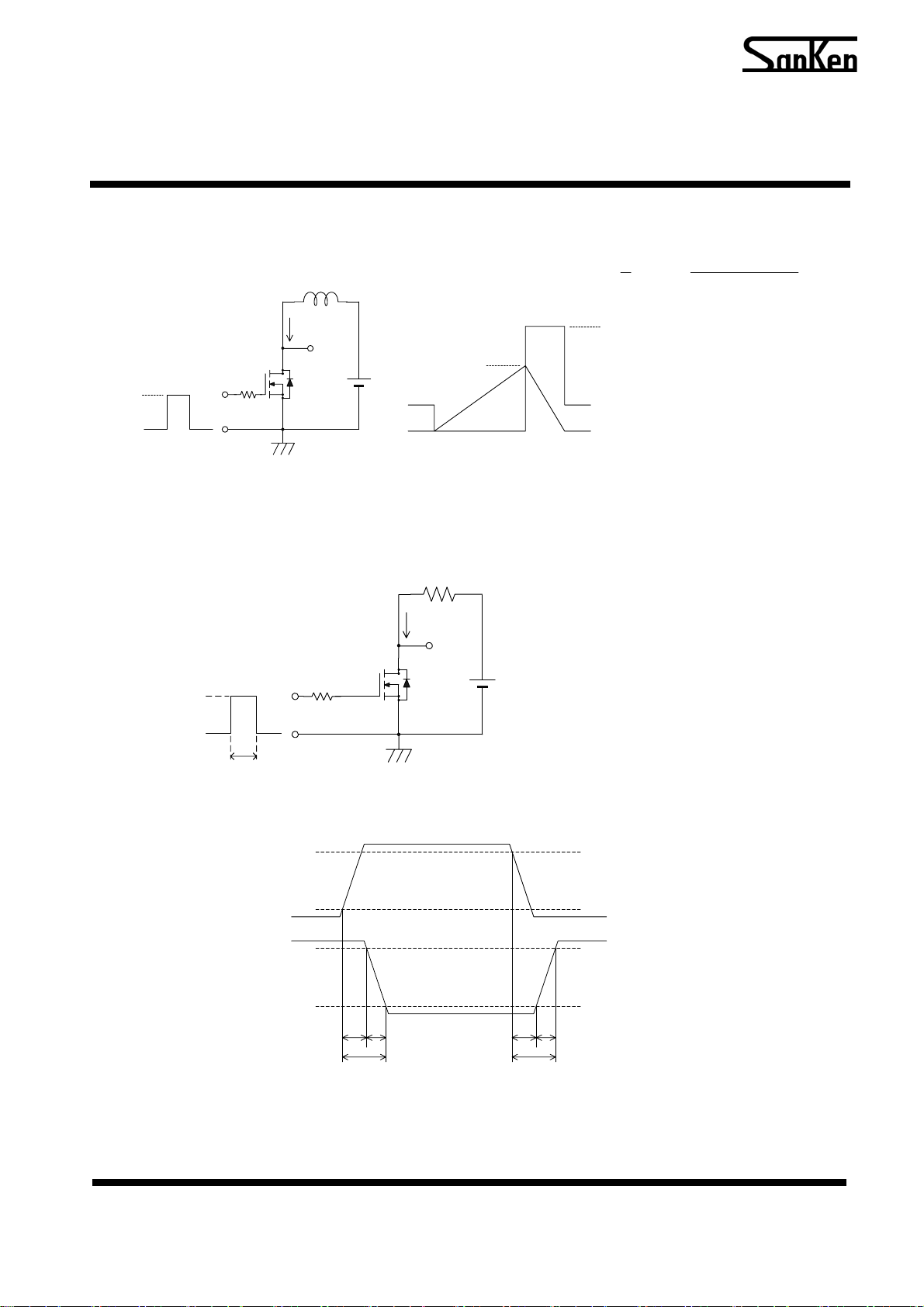
Fig.1 Unclamped Inductive Test Method
V
L
EAS=
1
•L•ILP2 •
2
(BR)DSS
−
DD(BR)DSS
VV
V
GS
0V
R
I
L
V
DS
I
G
V
DD
Lp
I
L
V
(BR)DSS
V
DS
V
DD
(a) Test Circuit (b) Waveforms
Fig.2 Switching Time Test Method
R
L
V
I
R
V
V
R
GS
0V
P.W.=10μs
Duty cycle≦1%
R
G
I
D
V
DS
(a) Test Circuit
V
DD
DD≈140V
D=20A
L=7Ω
GS=10V
G=5Ω
GS
V
90%
10%
V
DS
t
d(on)
t
r
t
on
t
d(off)
t
off
90%
10%
t
f
(b) Waveforms
Sanken Electric Co.,Ltd.
T02-001EA-050912
Page 6
6/9
N-Channel MOS FET
FKP280A September, 2005
Outline
FM100 (TO3P Full Mold)
Measured at the root
Measured at the root
Plane
Measured at the root
Side
(1) (2) (3)
Mass: Approx.6.5g
Sanken Electric Co.,Ltd.
T02-001EA-050912
Page 7
7/9
N-Channel MOS FET
FKP280A September, 2005
<Worldwide Contacts>
Asia Pacific
China
Sanken Electric Hong Kong Co., Ltd.
Suite 1026 Ocean Centre, Canton Road, Tsimshatsui, Kowloon, Hong Kong
Tel: 852-2735-5262
Fax: 852-2735-5494
Sanken Electric (Shanghai) Co., Ltd.
Room3202, Maxdo Centre, Xingyi Road 8, Changning district, Shanghai, China
Tel: 86-21-5208-1177
Fax: 86-21-5208-1757
Taiwan Sanken Electric Co., Ltd.
Room 1801, 18th Floor, 88 Jung Shiau East Road, Sec. 2, Taipei 100, Taiwan R.O.C.
Tel: 886-2-2356-8161
Fax: 886-2-2356-8261
India
Saket Devices Pvt. Ltd.
Office No.13, First Floor, Bandal - Dhankude Plaza, Near PMT Depot, Paud Road, Kothrud, Pune - 411 038, India
Tel: 91-20-5621-2340
91-20-2528-5449
Fax: 91-20-2528-5459
Japan
Sanken Electric Co., Ltd. Overseas Sales Headquaters
Metropolitan Plaza Bldg. 1-11-1 Nishi-Ikebukuro, Toshima-ku, Tokyo 171-0021, Japan
Tel: 81-3-3986-6164
Fax: 81-3-3986-8637
Korea
Sanken Electric Korea Co., Ltd.
Mirae Asset Life Bldg. 6F, 168 Kongduk-dong, Mapo-ku, Seoul, 121-705, Korea
Tel: 82-2-714-3700
Fax: 82-2-3272-2145
Singapore
Sanken Electric Singapore Pte. Ltd.
150 Beach Road, #14-03 The Gateway West, Singapore 189720
Tel: 65-6291-4755
Fax: 65-6297-1744
Sanken Electric Co.,Ltd.
T02-001EA-050912
Page 8

8/9
N-Channel MOS FET
FKP280A September, 2005
Europe
United Kingdom
Sanken Power Systems (UK) Limited
Pencoed Technology Park, Pencoed, Bridgend CF35 5HY. UK
Tel: 44-1656-869-100
Fax: 44-1656-869-162
North America
United States
Allegro MicroSystems, Inc.
115 Northeast Cutoff, Worcester, Massachusetts 01606, U.S.A.
Tel: 1-508-853-5000
Fax: 1-508-853-3353
Allegro MicroSystems, Inc. (Southern California)
14 Hughes Street, Suite B105, Irvine, CA 92618
Tel: 1-949-460-2003
Fax: 1-949-460-7837
Sanken Electric Co.,Ltd.
T02-001EA-050912
Page 9

9/9
N-Channel MOS FET
FKP280A September, 2005
CAUTION / WARNING
●The information in this publication has been carefully checked and is believed to be accurate; however, no responsibility
is assumed for inaccuracies.
● Sanken reserves the right to make changes without further notice to any products herein in the interest of improvements
in the performance, reliability, or manufacturability of its products.
Before placing an order, Sanken advises its customers to obtain the latest version of the relevant information to verify that
the information being relied upon is current.
● Application and operation examples described in this catalog are quoted for the sole purpose of reference for the use of
the products herein and Sanken can assume no responsibility for any infringement of industrial property rights,
intellectual property rights or any other rights of Sanken or any third party which may result from its use.
● When using the products herein, the applicability and suitability of such products for the intended purpose or object shall
be reviewed at the users’ responsibility.
● Although Sanken undertakes to enhance the quality and reliability of its products, the occurrence of failure nd defect of
semiconductor products at a certain rate is inevitable. Users of Sanken products are requested to take, at their own risk,
preventative measures including safety design of the equipment or systems against any possible injury, death, fires or
damages to the society due to device failure or malfunction.
● Sanken products listed in this catalog are designed and intended for the use as components in general purpose electronic
equipment or apparatus (home appliances, office equipment, telecommunication equipment, measuring equipment, etc.).
Before placing an order, the user’s written consent to the specifications is requested.
When considering the use of Sanken products in the applications where higher reliability is required (transportation
equipment and its control systems, traffic signal control systems or equipment, fire/crime alarm systems, various safety
devices, etc.), please contact your nearest Sanken sales representative to discuss and obtain written confirmation of your
specifications. The use of Sanken products without the written consent of Sanken in the applications where extremely
high reliability is required (aerospace equipment, nuclear power control systems, life support systems, etc.) is strictly
prohibited.
● Anti radioactive ray design is not considered for the products listed herein.
● This publication shall not be reproduced in whole or in part without prior written approval from Sanken.
●This is notification that you, as purchaser of the products/technology, are not allowed to perform any of the following:
1. Resell or retransfer these products/technology to any party intending to disturb international peace and security.
2. Use these products/technology yourself for activities disturbing international peace and security.
3. Allow any other party to use these products/technology for activities disturbing international peace and security.
Also, as purchaser of these products/technology, you agree to follow the procedures for the export or
transfer of these products/technology, under the Foreign Exchange and Foreign Trade Law, when you
export or transfer the products/technology abroad.
Sanken Electric Co.,Ltd.
T02-001EA-050912
 Loading...