

Datasheet FKC05-48S33W, FKC05-48S33, FKC05-48S15W, FKC05-48S15, FKC05-48S12W Datasheet (P-DUKE)
...Page 1
OUTPUT SPECIFICATIONS
Output power 5 Watts max
Voltage accuracy Full load and nominal Vin ± 2%
Minimum load (Note 1)
10% of FL
Line regulation LL to HL at Full Load
± 0.2%
Load regulation 25% to 100% FL
Single
Dual
± 0.5%
± 1%
Cross regulation(Dual) Asymmetrical load 25% / 100% FL ± 5%
Ripple and noise 20MHz bandwidth 50mVp-p
T e mperature coefficient
I0.02% / ºC, max
Transient response recovery time 25% load step change 200uS
Over load protection % of FL at nominal input 170% typ
Short circuit protection Continuous, automatics recovery
INPUT SPECIFICATIONS
Input voltage range
FKC05
FKC05-W
12V nominal input
24V nominal input
48V nominal input
24V nominal input
48V nominal input
9 – 18VDC
18 – 36VDC
36 – 75VDC
9 – 36VDC
18 – 75VDC
Input filter Pi type
Input surge voltage
100mS max
12V input
24V input
48V input
36VDC
50VDC
100VDC
Input reflected ripple (Note 2) Nominal Vin and full load 20mAp-p
Start up time Nominal Vin and constant resistor load 600mS typ
GENERAL SPECIFICATIONS
Efficiency See table
Isolation voltage
Input to Output
Input ( Output ) to Case
1600VDC, min
DIP 1600VDC, min
SMD 1000VDC, min
Isolation resistance
109ohms, min
Isolation capacitance 300pF, ma
x
Switching frequency 300KHz, typ
Approvals and standard IEC60950, UL1950, EN60950
Case material Nickel-coated coppe
r
Base material Non-conductive black plastic
Potting material Epoxy (UL94-V0)
Dimensions
1.25 X 0.80 X 0.40 Inch
(31.8 X 20.3 X 10.2 mm)
Weight
DIP
SMD
16g (0.55oz)
18g (0.62oz)
MTBF (Note 3) 3.165 x 10⁶ hrs
ENVIRO NMENTAL SPECIFIC ATIONS
Operating temperature range
Standard
M1 (Note 4)
M2 (W series)
-25ºC~+85ºC (with derating)
-40ºC~+85ºC (non-derating)
-40ºC~+85ºC (with derating)
Maximum case temperature +100ºC
Storage temperature range -55ºC ~ +105ºC
Thermal impedance Nature convection 20ºC/watt
Thermal shock MIL-STD-810D
Vibration 10~55Hz, 2G, 30minitues along X,Y and Z
Relative humidity 5% to 95% RH
EMC CHARACT ERIST ICS
Conducted emissions EN55022 Level A
Radiated emissions EN55022 Level A
ESD EN61000-4-2 Perf. Criteria
2
Radiated immunity EN61000-4-3 Perf. Criteria
2
Fast transient EN61000-4-4 Perf. Criteria
2
Surge EN61000-4-5 Perf. Criteria
2
Conducted immunity EN61000-4-6 Perf. Criteria
2
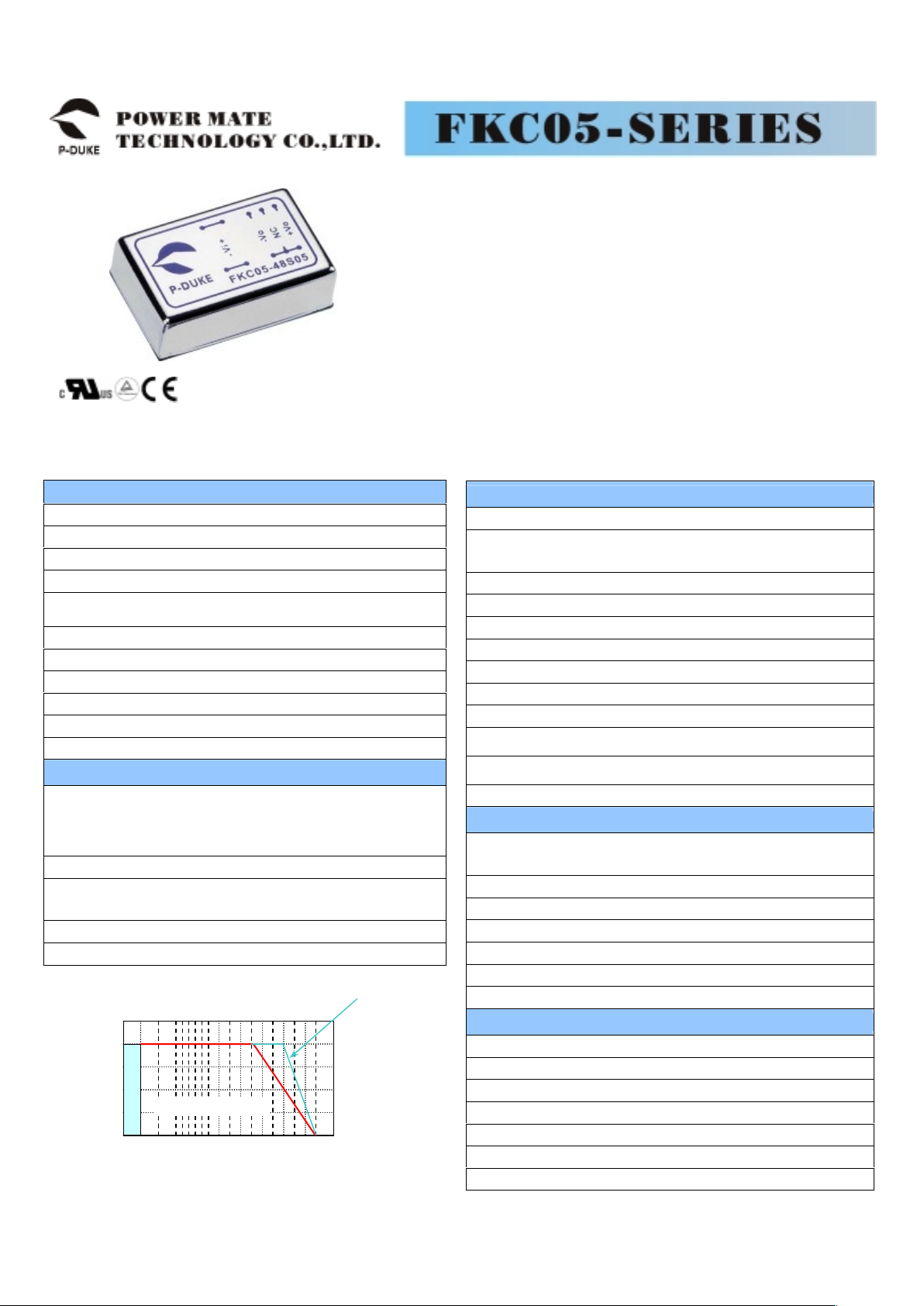
The FKC05 series offer 5 watts of output power from a package in an IC compatible
24pin DIP configuration without derating to 71ºC ambient temperature and pin to pin
compatible with FKC03 series. FKC05 series have 2:1 wide input voltage of 9-18, 18-36
and 36-75VDC. FKC05-W series have 4:1 ultra wide input voltage of 9-36 and
18-75VDC. The FKC05 features 1600VDC of isolation, short-circuit protection and as
well as five sided shielding. All models are particularly suited to telecommunications,
industrial, mobile telecom and test equipment applications.
TECHNICAL SPECIFICATION All specifications are typical at nominal input, full load and 25ºC otherwise noted
50 60 70 80 90
100 -40 -25 0 -10
25
50
75
100
0
AMBIENT TEM PERA TURE (ºC)
OUTPUT POWER (%)
FKC05-48S05 Derating Curve
Nature convection
M! Version
M1 Version
UL E193009
TUV R3-50007936
CB JPTUV-003641
CE MARK
• 5 WATTS OUTPUT POWER
• 2:1 AND 4:1 WIDE INPUT VOLTAGE RANGE
• INTERNATIONAL SAFETY STANDARD APPROVAL
• FIVE-SIDED SHIELD
• HIGH EFFICIENCY UP TO 84%
• STAN DARD 24 PIN DIP PACKAGE & SMD TYPE PACKAGE
• FIXED SWITCHING FREQUENCY
Page 2
Model
Number
Input
Range
Output
Voltage
Output
Current
Input
Current
(5)
Eff
(6)
(%)
Capacitor
(7)
Load max
FKC05-12S33 9 – 18 VDC 3.3 VDC 1000mA
382mA
76 2200uF
FKC05-12S05 9 – 18 VDC 5 VDC 1000mA
563mA
78 1000uF
FKC05-12S12 9 – 18 VDC 12 VDC 470mA 603mA 82 220uF
FKC05-12S15 9 – 18 VDC 15 VDC 400mA 649mA 81 150uF
FKC05-12D05 9 – 18 VDC ± 5 VDC ± 500mA 563mA 78 ± 680uF
FKC05-12D12 9 – 18 VDC ± 12 VDC ± 230mA 597mA 81 ± 100uF
FKC05-12D15 9 – 18 VDC ± 15 VDC ± 190mA 617mA 81 ± 68uF
FKC05-24S33 (W) 18 – 36 (9 – 36) VDC 3.3 VDC 1000mA 194mA (191mA) 75 (76) 2200uF
FKC05-24S05 (W) 18 – 36 (9 – 36) VDC 5 VDC 1000mA 285mA (285mA) 77 (77) 1000uF
FKC05-24S12 (W) 18 – 36 (9 – 36) VDC 12 VDC 470mA 305mA (309mA) 81 (80) 220uF
FKC05-24S15 (W) 18 – 36 (9 – 36) VDC 15 VDC 400mA 325mA (329mA) 81 (80) 150uF
FKC05-24D05 (W) 18 – 36 (9 – 36) VDC ± 5 VDC ± 500mA 274mA (282mA) 80 (78) ± 680uF
FKC05-24D12 (W) 18 – 36 (9 – 36) VDC ± 12 VDC ± 230mA 288mA (295mA) 84 (82) ± 100uF
FKC05-24D15 (W) 18 – 36 (9 – 36) VDC ± 15 VDC ± 190mA 308mA (313mA) 81 (80) ± 68uF
FKC05-48S33 (W) 36 – 75 (18 – 75) VDC 3.3 VDC 1000mA 98mA (100mA) 74 (73) 2200uF
FKC05-48S05 (W) 36 – 75 (18 – 75) VDC 5 VDC 1000mA 143mA (145mA) 77 (76) 1000uF
FKC05-48S12 (W) 36 – 75 (18 – 75) VDC 12 VDC 470mA 151mA (155mA) 82 (80) 220uF
FKC05-48S15 (W) 36 – 75 (18 – 75) VDC 15 VDC 400mA 162mA (167mA) 81 (79) 150uF
FKC05-48D05 (W) 36 – 75 (18 – 75) VDC ± 5 VDC ± 500mA 141mA (145mA) 78 (76) ± 680uF
FKC05-48D12 (W) 36 – 75 (18 – 75) VDC ± 12 VDC ± 230mA 147mA (151mA) 82 (80) ± 100uF
FKC05-48D15 (W) 36 – 75 (18 – 75) VDC ± 15 VDC ± 190mA 154mA (159mA) 81 (79) ± 68uF
Note
1. The FKC05 (W) series required a minimum 10% loading on the output to maintain specified regulation. Operation under no-load condition will not damage
these devices, however they may not meet all listed specification.
2. Simulated source impedance of 12uH. 12uH inductor on series with + Vin.
3. BELLCORE TR-NWT-000332. Case I: 50% Stress, Temperature at 40ºC. (Ground fixed and controlled environment)
4. M1 version is more efficient, therefore, it can be operated in a more extensive temperature range than standard and M2 version
5. Maximum value at nominal input voltage and full load of standard type.
6. Typical value at nominal input voltage and full load
7. Test by minimum Vin and constant resistor load.
8. There is no pin at PIN10 & PIN15 for FKC05-W series
DIP PIN CONNECTI ON
PIN SINGLE DUAL
2 - INPUT - INPUT
3 - INPUT - INPUT
9 NC
COMMON
23 + INPUT + INPUT
22 + INPUT + INPUT
16 - OUTPUT COMMON
10 NC(Note 8) NC(Note 8) 15 NC(Note 8) NC(Note 8)
PIN SINGLE DUAL
11 NC - OUT P U T 14 + OUTPUT + OUTPUT
SMD PIN CONNECTI ON
PIN SINGLE DUAL
2 - INPUT - INPUT
3 - INPUT - INPUT
9 NC
COMMON
23 + INPUT + INPUT
22 + INPUT + INPUT
16 - OUTPUT COMMON
10 NC NC 15 NC NC
PIN SINGLE DUAL
11 NC - OUTPUT 14 + OUTPUT + OUTPUT
Others NC NC Others NC NC
1. All dimensions in Inches (mm)
2. Pin pitch tolerance I0.014(0.35)
Pin size is 0.02( 0.5) Dia or
0.01 x 0.02 (0.25 x 0.50) Rectan gular Pin
14
23
22
16
3
9
2
11
1.25 (31.8)
0.60(15.2)
0.80(20.3)
0.40
(10.2)
0.15
(3.8)
0.70 (17.8)
0.20 (5.1)
0.18(4.6)
BOT TOM
VIEW
15
10
Suffix-SMD
1.00(25.4)
0.92(23.4)
0.44(11.2)
0.43(10.9)
0.10 (2.54)
0.15 (3.81) 0.25 (6.35)
1.25 (31.8)
0.80(20.3)
0.02(0.5)
24
13
16
20
12
1
5
9
BOTTOM
VIEW
Pin Area
0.04 x 0.02
(1.0 x 0.5)
 Loading...