

Page 1
December 2001
Revised December 2001
FIN1532
5V LVDS 4-Bit High Speed Differential Receiver
FIN1532 5V LVDS 4-Bit High Speed Differential Receiver
General Description
This quad receiver is designed for high speed interconnects utilizing Low Voltage Differential Signaling (LVDS)
technology. The receiver translates LVDS levels, with a typical differential input th reshold of 1 00 mV, to LVTTL signal
levels. LVDS provides low EMI at ultra low power dissipation even at high frequen cies. This device is ideal for high
speed transfer of clock and data.
The FIN1532 can be paired with its companion dr iver, the
FIN1531, or any other LVDS driver.
Features
■ Greater than 400Mbs data rate
■ 5V power su pply operation
■ 0.5 ns maximum differential pulse skew
■ 3 ns maximum propagation delay
■ Low power dissipation
■ Power-Off protection for inputs and outputs
■ Fail safe protection for ope n-circuit, shorted and termi-
nated receiver inputs
■ Meets or exceeds the TIA/EIA-644 LVDS standard
■ Pin compatible with equivalent RS-422
and PECL devices
■ 16-Lead SOIC and TSSOP packages save space
Ordering Code:
Order Number Package Number Package Description
FIN1532M M16A 16-Lead Small Outline Integrated Circuit (SOIC), JEDEC MS-012, 0.150" Narrow
FIN1532MTC MTC16 16-Lead Thin Shrink Small Outline Package (TSSOP), JEDEC MO-153, 4.4mm Wide
Devices also availab le in Tape and Reel. Specify by appending the suffix letter “X” to the o rdering code.
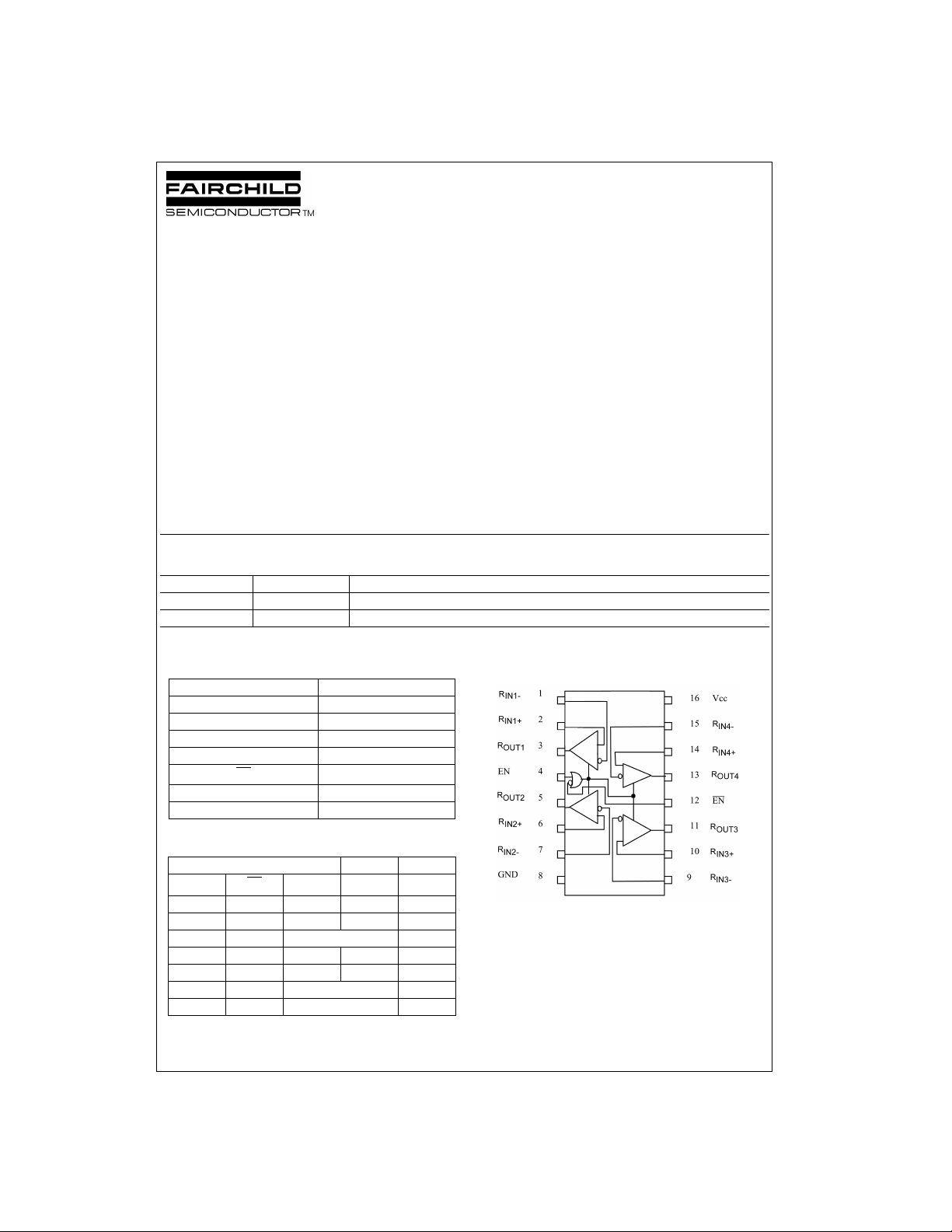
Pin Descriptions
Pin Name Description
R
, R
, R
OUT1
R
IN1+
R
IN1−
, R
, R
OUT2
IN2+
IN2−
, R
OUT3
, R
, R
IN3+
IN4+
, R
, R
IN3−
EN Driver Enable Pin
EN
V
GND Ground
IN4−
CC
LVTTL Data Outputs
OUT4
Non-inverting LVDS Inputs
Inverting LVDS Inputs
Inverting Driver Enable Pin
Power Supply
Connection Diagram
Function Table
Input Outputs
EN EN
HXHLH
HXLHL
H X Fail Safe Condition H
XLHLH
XLLHL
X L Fail Safe Condition H
LH X Z
H = HIGH Logic Le v el L = LOW Logic Leve l X = Don’t Care
Z = High Impedance Fail Safe = Open, Shorted, Terminat ed
© 2001 Fairchild Semiconductor Corporation DS500504 www.fairchildsemi.com
R
IN+
R
IN+
R
OUT
Top View
Page 2
Absolute Maximum Ratings(Note 1) Recommended Operating
Supply Voltage ( VCC) −0.5 V to +6 V
DC Input Voltage (V
FIN1532
Enable Inputs
Receiver Inputs
DC Output Voltage (V
DC Output Current (I
Storage Temperature Range (T
Max Junction Temperature (T
Lead Temperature (T
)
IN
−0.5 V to +6 V
−0.5 V to +6 V
) −0.5 V to +6 V
OUT
)16 mA
O
)
L
) −65°C to +150°C
STG
)150°C
J
(Soldering, 10 seconds) 260
ESD (Human Body Model)
ESD (Machine Model)
≥ 8000 V
≥ 300 V
Conditions
Supply Voltage (V
Input Voltage (V
Enable Inputs 0 to V
Receiver Inputs 0 to 2.4 V
Magnitude of Differential Voltage
(|V
|) 100 mV to 600 mV
ID
Common-mode Input Voltage
)|V
(V
°C
IC
Operating Temperature (T
Note 1: The “Absolute Maximum Ratings”: are those values beyond which
damage to the device may occur. The databook specifications should be
met, without exception, to ensure that the system design is reliable over its
power supply, temperatur e and output/input loading va riables. Fairchild
does not recommend operation of circu it s o ut s ide databook specific ation.
) 4.5 V to 5.5 V
CC
)
IN
) −40°C to +85°C
A
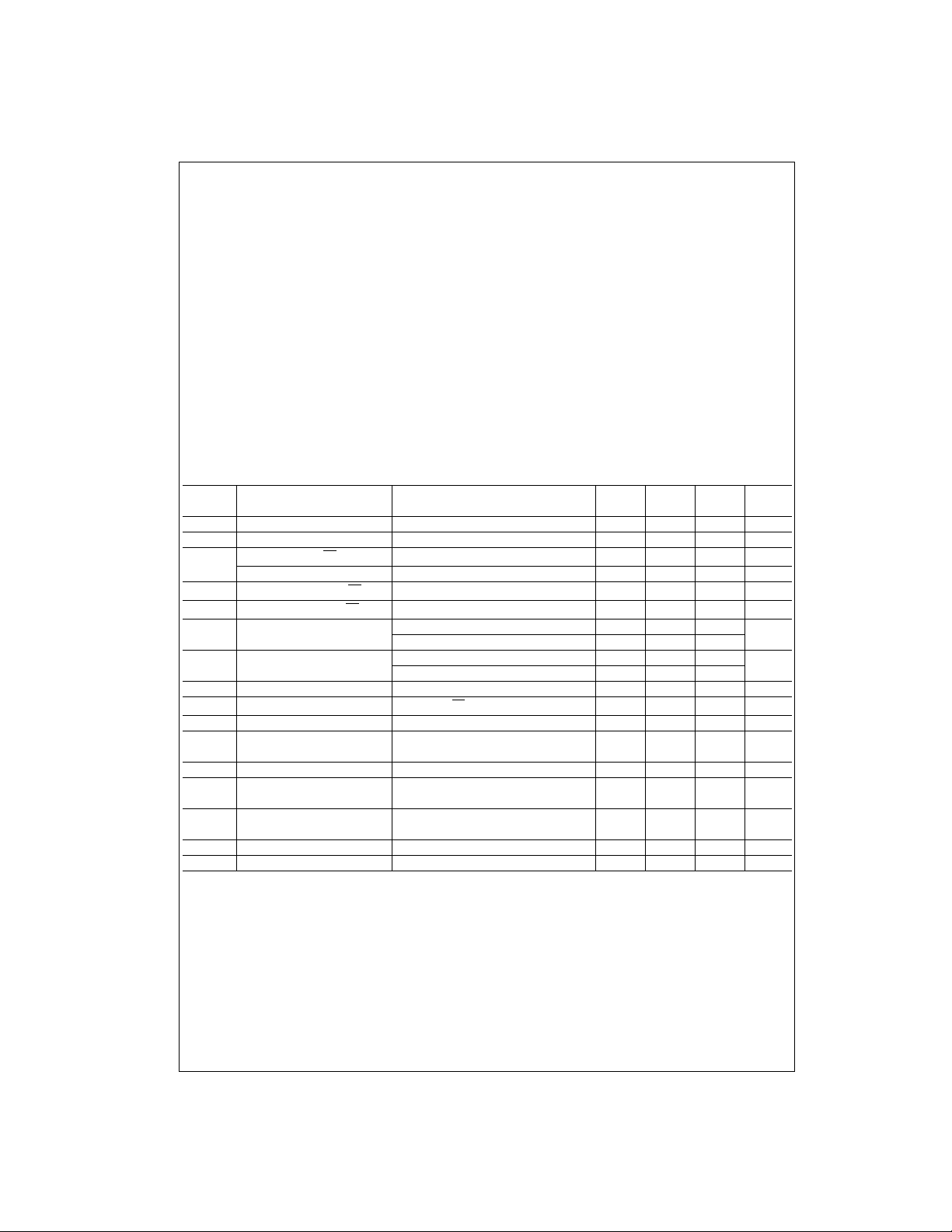
DC Electrical Characteristics
Over supply voltage and operating temperature ranges, unless otherwise specified
Symbol Parameter Test Conditions
V
TH
V
TL
I
IN
V
IH
V
IL
V
OH
V
OL
V
IK
I
OZ
I
O(OFF)
I
OS
I
CCZ
I
CC
I
PU/PD
C
IN
C
OUT
Note 2: All typical values are at TA = 25°C and with VCC = 5V.
Differential Input Threshold HIGH VIC = +1.2V, See Figure 1 100 mV
Differential Input Threshold LOW VIC = +1.2V, See Figure 1 −100 mV
Input Current EN or EN VIN = 0V or VCC, VCC = 5.5 or 0V ±20 µA
Input Current Receiver Inputs V
Input High Voltage (EN or EN)2.0V
Input Low Voltage (EN or EN)GND0.8V
Output HIGH Voltage IOH = −100 µAV
Output LOW Voltage IOH = 100 µA0.010.2
Input Clamp Voltage IIK = −18 mA −1.5 −0.8 V
Disabled Output Leakage Current EN = 0.8 and EN = 2V, V
Power-OFF Output Current V
Output Short Circuit Test Receiver Enabled, V
Disabled Power Supply Current Receiver Disabled 1.2 5 mA
Power Supply Current Receiver Enabled, R
Output Power Up/Power Down VCC = 0V to 2.0V ±20 µA
High Z Leakage Current
Input Capacitance 5.5 pF
Output Capacitance 4.5 pF
= 0V or 2.4 V, VCC = 5.5 or 0V ±20 µA
IN
IOH = −8 mA 3.8 4.68
= 8 mA 0.22 0.5
I
OL
= 0V or 5.5V, VCC = 0V 50 µA
OUT
(one output shorted at a time)
Receiver Enabled, R
OUT
= 0V
OUT
= 1V and R
IN+
= 1.4V and R
IN+
= 5.5V or 0V ±20 µA
= 1.4V 11 17
IN−
= 1V 15 23
IN−
Min Typ Max
−0.2 4.98
CC
−15 −100 mA
(Note 2)
|/2 to (2.4−|VID|/2)
ID
CC
CC
Units
V
V
V
mA
www.fairchildsemi.com 2
Page 3

AC Electrical Characteristics
Over supply voltage and operating temperature ranges, unless otherwise specified
Symbol Parameter Test Conditions
t
PLH
Propagation Delay
LOW-to-HIGH
t
PHL
t
TLH
t
THL
t
SK(P)
t
SK(LH)
t
SK(HL)
t
SK(PP)
f
MAX
Propagation Delay
HIGH-to-LOW |V
| = 400 mV, CL = 10 pF, RL = 1kΩ
ID
Output Rise Time (20% to 80%) See Figure 1 and Figure 2 1.3 ns
Output Fall Time (80% to 20%) 1.1 ns
Pulse Skew |t
- t
| 0.2 0.5 ns
PLH
PHL
, Channel-to-Channel Skew
(Note 4)
Part-to-Part Skew (Note 5) 1.0 ns
Maximum Operating Frequency RL = 1kΩ, CL = 10 pF,
(Note 6) See Figure 1 and Figure 2
t
ZH
t
ZL
t
HZ
t
LZ
Note 3: All typical values are at TA = 25°C and with VCC = 5V.
Note 4: t
tion.
Note 5: t
(either LOW-to-HIGH or HIGH-to-LOW) when both devices operate with the same supply voltage, same temperature, and have identical test circuits.
Note 6: f
All channels switchin g in phase.
LVTTL Output Enable Time from Z to HIGH RL = 1kΩ, CL = 10 pF, 8 12.0 ns
LVTTL Output Enable Time from Z to LOW See Figure 3 and Figure 4 8 12.0 ns
LVTTL Output Di sable Time from HIGH to Z 4 8.0 ns
LVTTL Output Disable Time from LOW to Z 4 8.0 ns
, t
SK(LH)
SK(PP)
MAX
is the skew between spe cifi ed out puts of a sing le dev ice whe n the ou tput s have iden tical lo ads an d ar e switch ing in the sam e direc-
SK(HL)
is the magnitude of t he difference in propagation delay tim es between any sp ec if ied terminals of two devices switching in the same direction
Criteria: Input tR = tF < 1 ns, VID = 300 mV, (1.05V to 1.35V pp), 50% duty cycle; Output duty cycle 40% to 60%, VOL < 0.5V , VOH > 2.4V.
Min Typ Max
(Note 3)
1.0 2.0 3.0 ns
1.0 2.0 3.0 ns
0.1 0.3 ns
200 260 MHz
FIN1532
Units
Note A: All input pulses have frequ ency = 10 MHz, t
Note B: C
includes all probe and jig capacitances
L
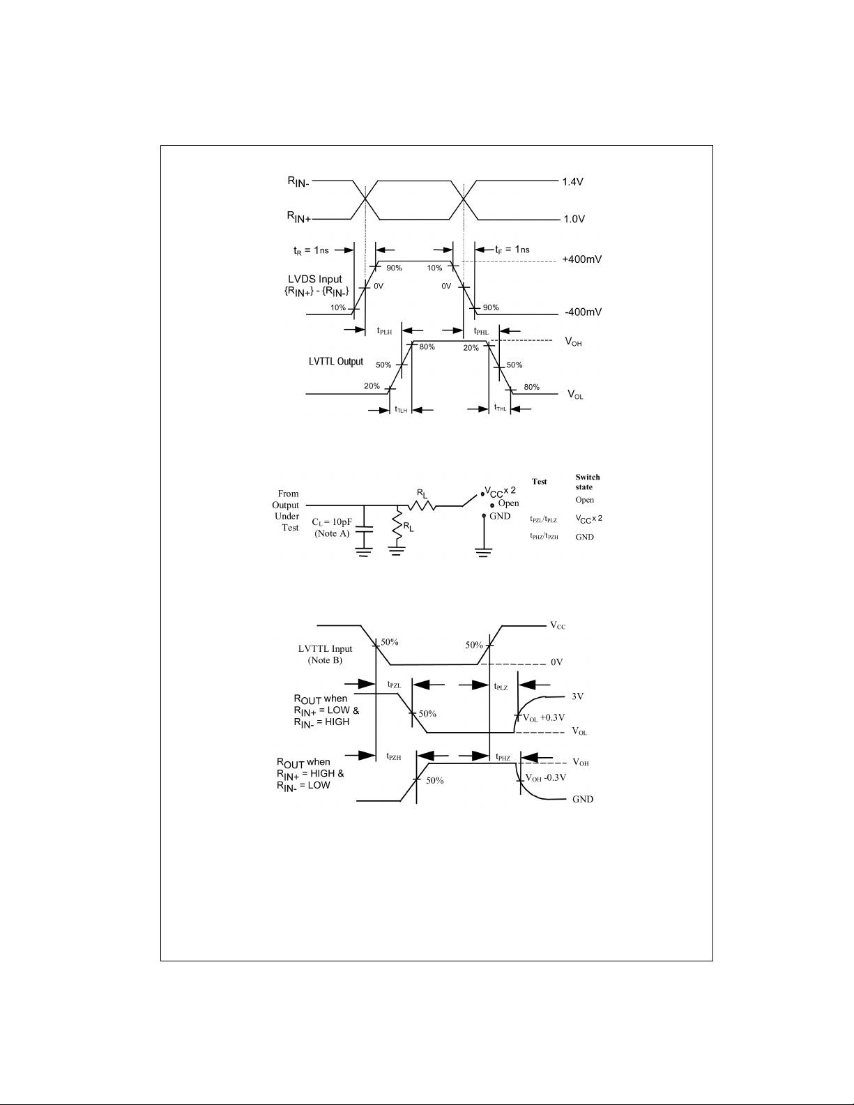
FIGURE 1. Differential Receiver Voltage Definitions and Propagation Delay
or tF = 1 ns
R
3 www.fairchildsemi.com
Page 4
FIN1532
FIGURE 2. LVDS Input to LVTTL Output AC Waveforms
Test Circuit for LVTTL Outputs
FIGURE 3. AC Loading Circuit for LVTTL Outputs
Voltage Wa veforms Enable and Disable Times
Note A: CL includes probes and jig capacitance
Note B: All LVTTL input pulses have the following characteristics: Frequency = 10 MHz, t
FIGURE 4. LVTTL Outputs Test Circuit and AC Waveforms
www.fairchildsemi.com 4
or tF = 2 ns
R
Page 5
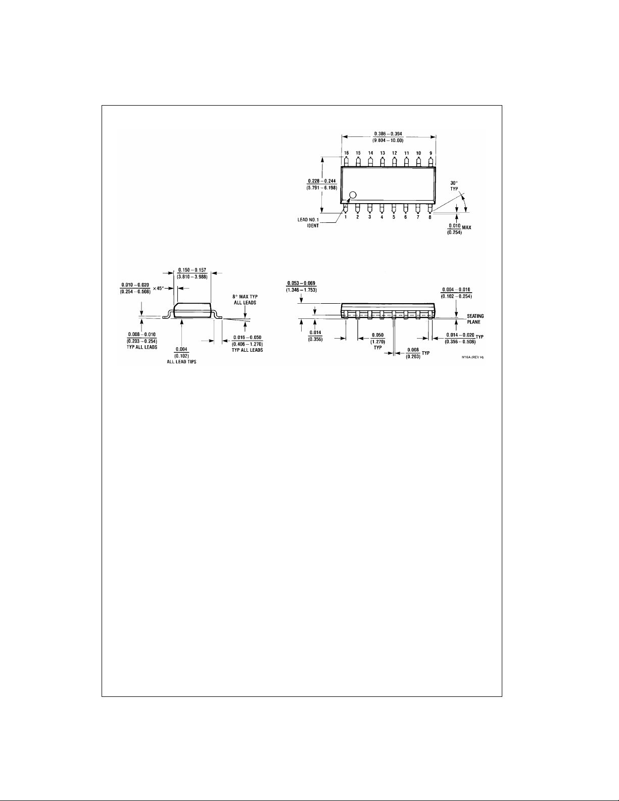
Physical Dimensions inches (millimeters) unless otherwise noted
FIN1532
16-Lead Small Outline Integrated Circuit (SOIC), JEDEC MS-012, 0.150" Narrow
Package Number M16A
5 www.fairchildsemi.com
Page 6

Physical Dimensions inches (millimeters) unless otherwise noted (Continued)
FIN1532 5V LVDS 4-Bit High Speed Differential Receiver
16-Lead Thin Shrink Small Outline Package (TSSOP), JEDEC MO-153, 4.4mm Wide
Fairchild does not assume any responsibility for use of any circuitr y described, no circuit patent licenses are implied a nd
Fairchild reserves the right at any time without notice to change said circuitry and specifications.
LIFE SUPPORT POLICY
FAIRCHILD’S PRODUCTS ARE NOT AUTHORIZED FOR USE AS CRITICAL COMPONENTS IN LIFE SUPPORT
DEVICES OR SYSTEMS WITHOUT THE EXPRESS WRITTEN APPROVAL OF THE PRESIDENT OF FAIRCHILD
SEMICONDUCTOR CORPORATION. As used herein:
1. Life suppor t de vices o r syste ms are device s or syste ms
which, (a) are intended for surgical implant into the
body, or (b) support or sustain life, and (c) whose failure
to perform when properly used in accordance with
instructions for use provided in the labeling, can be reasonably expected to result in a significant inju ry to the
user.
www.fairchildsemi.com 6
Package Number MTC16
2. A critical compon ent in any compon ent of a lif e supp ort
device or system whose failu re to perform can be reasonably expected to cause the failure of the li fe su pp ort
device or system, or to affect its safety or effectiveness.
www.fairchildsemi.com
 Loading...