

Page 1
FIN1108 • FIN1108T (Preliminary)
LVDS 8 Port High Speed Repeater
FIN1 108 • FIN1108T (Preliminary) LVDS 8 Port High Speed Repeater
March 2002
Revised May 2003
General Description
This 8 port repeater is designed for high speed interco nnects utilizing Low Voltage Differential Signaling (LVDS)
technology.
The FIN1108 accepts and outputs LVDS levels with a typi cal differential output swing of 330 mV w hich pro vides low
EMI at ultra low po wer dissipation even at hig h frequencies. The FIN1108 provides a V
pling on the inputs . In addition the FIN1108 can directly
accept LVPECL, HSTL, and SSTL-2 for translation to
LVDS.
The FIN1108T has internal termination across the receiver
inputs for reduced part count, reduced stub length and better noise immunity. See Applications section.
reference for AC co u-
BB
Features
■ Greater than 800 Mbps data rate
■ 3.3V power supply operation
■ 3.5 ps maximum random jitter and 135 ps maximum
deterministic jitter
■ Wide rail-to-rail common mode range
■ LVDS receiver inputs accept LVPECL, HSTL, and
SSTL-2 directly
■ Ultra low power consumption
■ 20 ps typical channel-to-chann el skew
■ Power off protection
■
> 7.5 kV HBM ESD Protection
■ Meets or exceeds the TIA/EIA-644-A LVDS standard
■ Available in space saving 48-lead TSSOP package
■ Open circuit fail safe protection
■ V
reference output
BB
■ FIN1108T (R
) features Internal Termination Resistors
T
Ordering Code:
Order Number Package Number Package Description
FIN1108MTD MTD48 48-Lead Thin Shrink Small Outline Package (TSSOP), JEDEC MO-153, 6.1mm Wide
FIN1108TMTD
(Preliminary)
Devices also availab l e in Tape and Reel. Specify by appending su ffix let te r “X” to the ordering code.
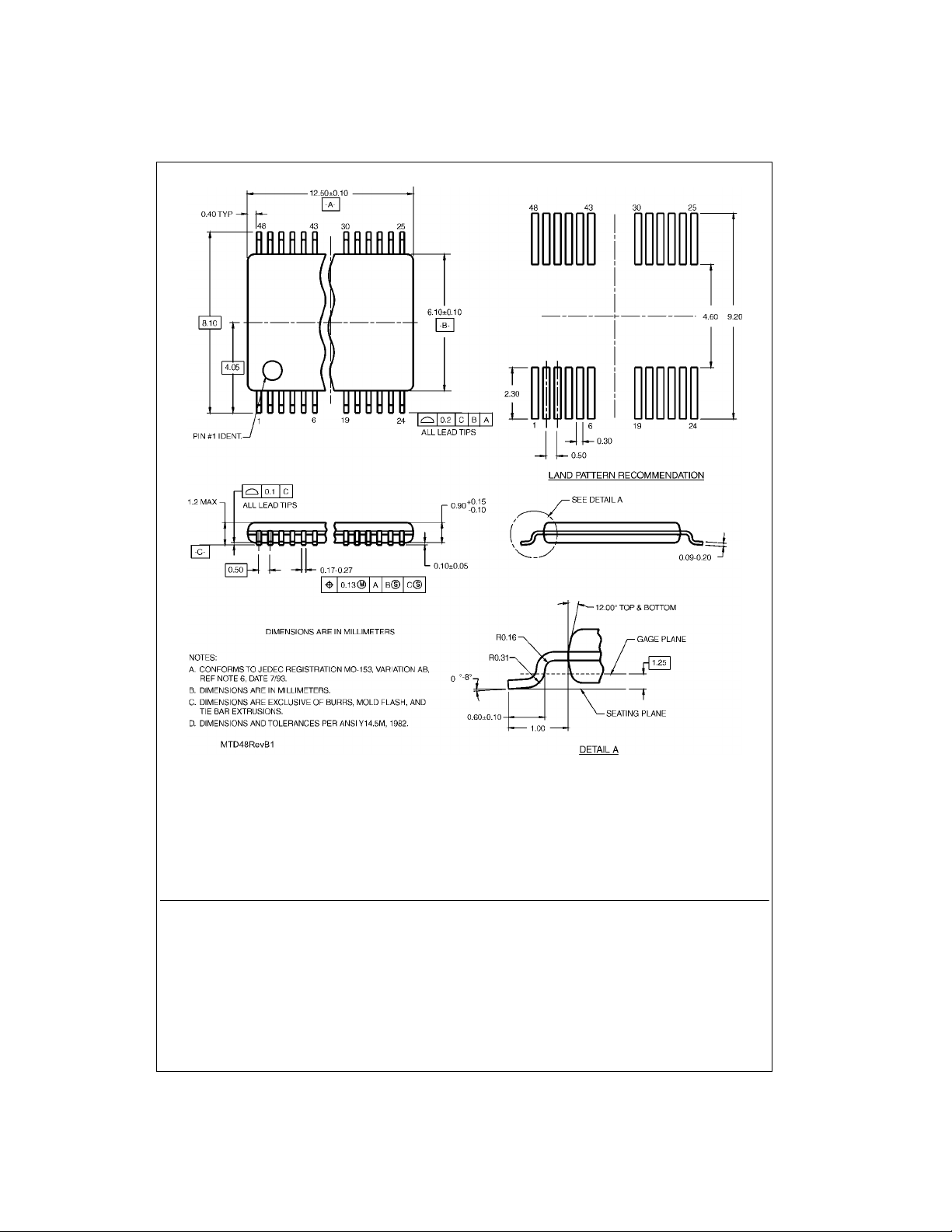
MTD48 48-Lead Thin Shrink Small Outline Package (TSSOP), JEDEC MO-153, 6.1mm Wide
© 2003 Fairchild Semiconductor Corporation DS500655 www.fairchildsemi.com
Page 2
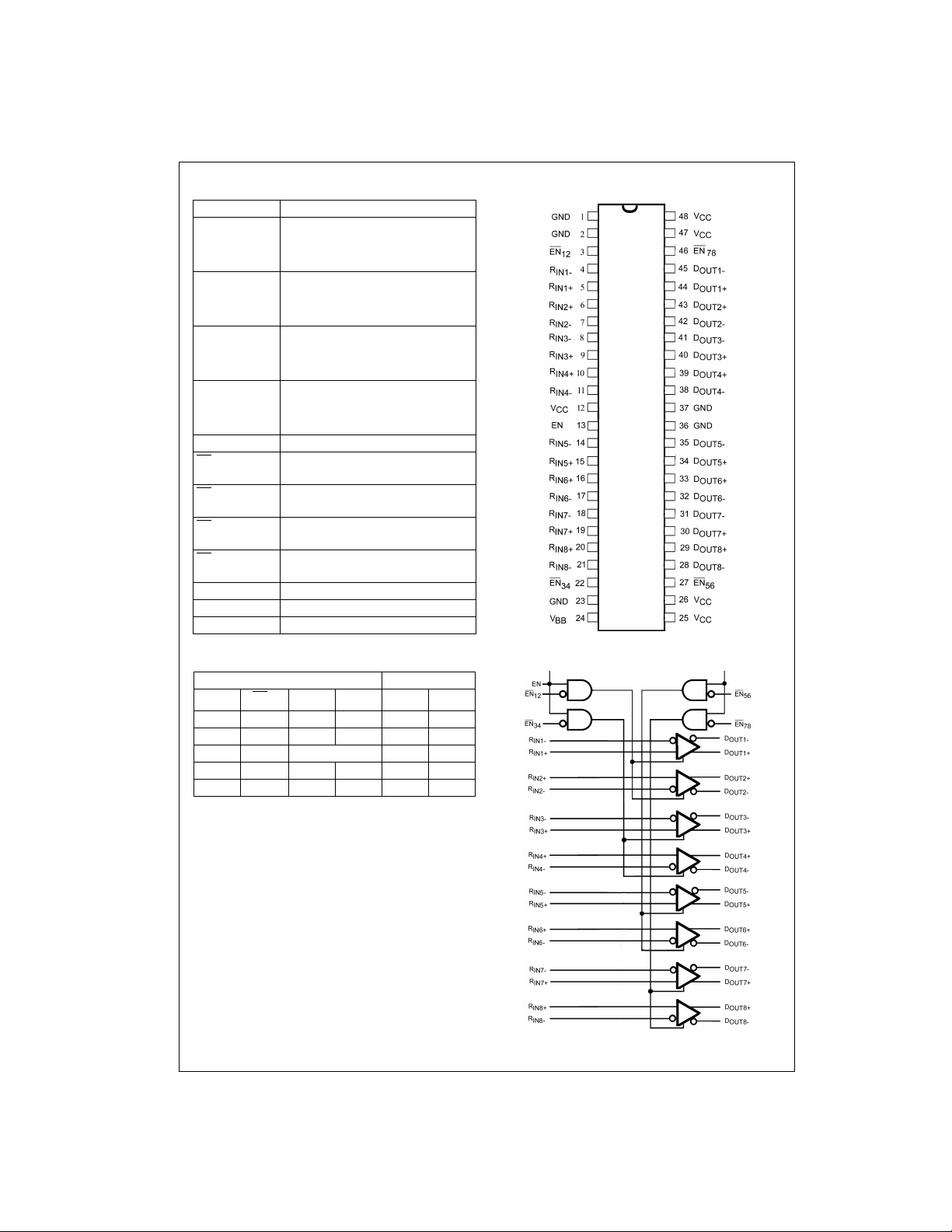
Pin Descriptions
Pin Name Description
R
, R
,
IN1+
IN2+
, R
R
IN3+
IN4+
R
, R
IN5+
IN6+
, R
R
IN7+
IN8+
R
, R
IN1−
IN2−
R
, R
IN3−
IN4−
, R
R
IN5−
IN6−
, R
R
IN7−
IN8−
D
, D
OUT1+
, D
D
OUT3+
, D
D
OUT5+
D
, D
OUT7+
D
, D
OUT1−
, D
D
OUT3−
D
, D
OUT5−
FIN1108 • FIN1108T (Preliminary)
D
OUT7−
, D
EN Driver Enable Pin for All Output
EN
12
EN
34
EN
56
EN
78
V
CC
GND Ground
V
BB
Non-inverting LVDS Input
,
,
,
Inverting LVDS Input
,
,
,
Non-inverting Driver Output
OUT2+
,
OUT4+
,
OUT6+
OUT8+
,
Inverting Driver Output
OUT2−
,
OUT4−
,
OUT6−
OUT8−
Inverting Driver Enable Pin for
and D
D
OUT1
Inverting Driver Enable Pin for
and D
D
OUT3
Inverting Driver Enable Pin for
and D
D
OUT5
Inverting Driver Enable Pin for
and D
D
OUT7
Power Supply
Reference Voltage Output
OUT2
OUT4
OUT6
OUT8
Connection Diagram
Function Table
Inputs Outputs
EN
EN
HL HLHL
HL LHLH
H L Fail Safe Case H L
XHXXZZ
LXXXZZ
H = HIGH Logic Level
L = LOW Logic Level
X = Don’t Care
Z = High Impedance
www.fairchildsemi.com 2
D
IN+
D
IN−DOUT+DOUT−
xx
Functional Diagram
Page 3

Applications
Signal Optimization via Internal Termination
For LVDS signaling in point-to-point applications, receivers
or repeaters with on-chip termination are preferable to
reduce the overshoot or undersho ot due to the reflection
caused by stubs at receiver inputs. As a rule of thumb, usually the termination resistor for an LVDS receiver should be
placed as close as pos sible to the receiver, especially f or
high speed application s. If the distance between ter mination resistors and re ceivers i s too lon g, the in terc onnect ion
will be seen as an un-terminated stub which can produce
reflections resulting in h igher EM I. Inte rnal term ination c an
effectively smooth out this ringing which can otherwise
jeopardize the recei ver nois e margin. T his is impor tant for
Advantages: Disadvantages:
1. Reduced device count resulting in reduced board space
and production cost.
2. Reduced reflections caused by the stub length on the
receiver inputs, improving the signal integrity.
reliable high-speed operation with tighter required signal
settling times. Belo w is a list of the advan tages/disadvantages of internal termination.
Internal termination is not suitable for all ap plications. In
order to set a proper V
with on-chip termination resistors only work for point-topoint applications since multi-drop applications would
require terminatio n resistor for ea ch receiver, reducing the
equivalent termination to R
output swing by n.
1. Without special process treatment, on-chip termination can
experience greater temperature variation. This is usually
tolerable for low speed applications that have a sufficient
unit interval.
2. For applications with high common-mode noise, a center
tapped capacitor at the receiver side is desirable to filter
out the common-mode voltage noise of the input LVDS signal. This scheme works for an external termination scheme
with two (50
half-value termination resistors connected in series and
center tapped to a capacitor to Ground. To implement this
scheme using internal termina tion resistors, a center tap
pin would have to be used. This would increase the package size of the part.
at the driver outputs, receiv ers
OD
. This would re duc e t h e dr iv e r
T/n
Ω each for nominal 100Ω termination resistor)
FIN1108 • FIN1108T (Preliminary)
3 www.fairchildsemi.com
Page 4
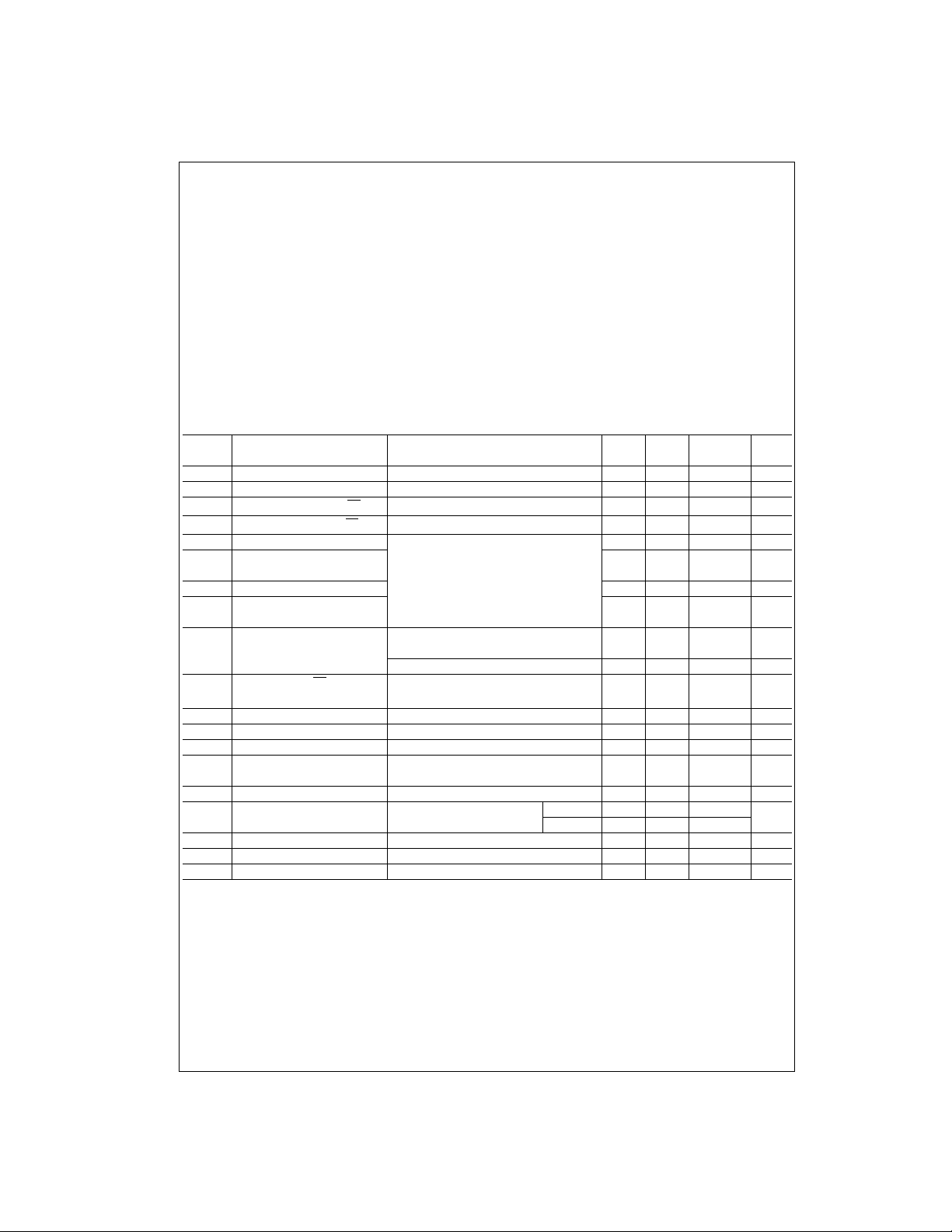
Absolute Maximum Ratings(Note 1) Recommended Operating
Supply Voltage (VCC) −0.5V to +4.6V
LVDS DC Input Voltage (V
LVDS DC Output Voltage (V
Driver Short Circuit Current (I
Storage Temperature Range (T
Max Junction Temperature (T
Lead Temperature (T
) −0.5V to +4.6V
IN
) −0.5V to +4.6V
OUT
) Continuous 10 mA
OSD
) −65°C to +150°C
STG
)150°C
J
)
L
(Soldering, 10 seconds) 260
ESD (Human B ody Model) 7500V
ESD (Machine Model) 400V
DC Electrical Characteristics
FIN1108 • FIN1108T (Preliminary)
Symbol Parameter Test Conditions
V
V
V
V
V
∆V
V
∆V
I
I
I
I
I
I
V
C
C
V
R
Differential Input Threshold HIGH See Figure 1; VIC = +0.05V, + 1.2V, or VCC − 0.05V 100 mV
TH
Differential Input Threshold LOW See Figure 1; VIC = +0.05V, + 1.2V, or VCC − 0.05V −100 mV
TL
Input HIGH Voltage (EN or EN)2.0V
IH
Input LOW Voltage (EN or EN)GND0.8V
IL
Output Differential Voltage 250 330 450 mV
OD
V
OD
OS
OS
OS
IN
OFF
CCZ
CC
OZ
IC
IN
OUT
BB
T
Note 2: All typical values are at TA = 25°C and with VCC = 3.3V .
Magnitude Change from
OD
Differential LOW-to-HIGH R
Offset Voltage See Figure 2 1.125 1.23 1.375 V
Offset Magnitude Change from
Differential LOW-to-HIGH
Short Circuit Output Current D
Input Current (EN, EN, D
Power Off Input or Output Current VCC = 0V, VIN or V
Disabled Power Supply Current Drivers Disabled 20 mA
Power Supply Current Drivers Enabled, Any Valid Input Condition 80 mA
Disabled Output Leakage Current Driver Disabled, D
Common Mode Voltage Range VID/2 VCC − (VID/2) V
Input Capacitance Enable Input 3
Output Capacitance 3pF
Output Reference Voltage VCC = 3.3V, IBB = 0 to −275 µA 1.125 1.2 1.375 V
Terminating Resistance 100 Ω
INx+
, D
= 100 Ω, Driver Enabled,
L
OUT+
Driver Enabled
VOD = 0V, Driver Enabled ±3.4 ±6mA
= 0V to VCC, Other Input = VCC or 0V
INx−)VIN
(for Differential Inputs)
D
OUT−
= 0V and D
= 0V to 3.6V
Conditions
Supply Voltage (V
Magnitude of Differential
Voltage (|V
Common Mode Voltage
Range (V
Operating Temperature (T
°C
Note 1: The “Absolute Maximum Ratings”: are those values beyond which
damage to the device may occur. The databook specifications should be
met, without exception, to ensure that the system design is reliable over its
power supply, temperatur e and output/input loading va riables. Fairchild
does not recommend operation of circu it s o ut s ide databook specific ation.
= 0V,
OUT−
= 0V to 3.6V ±20 µA
OUT
= 0V to 3.6V or
OUT+
LVDS Input 3
) 3.0V to 3.6V
CC
|) 100 mV to V
ID
)(0V + |VID|/2) to (VCC − |VID|/2)
IC
) −40°C to +85°C
A
Min Typ Max
(Note 2)
CC
Units
CC
25 mV
25 mV
−3.4 −6mA
±20 µA
±20 µA
V
pF
www.fairchildsemi.com 4
Page 5
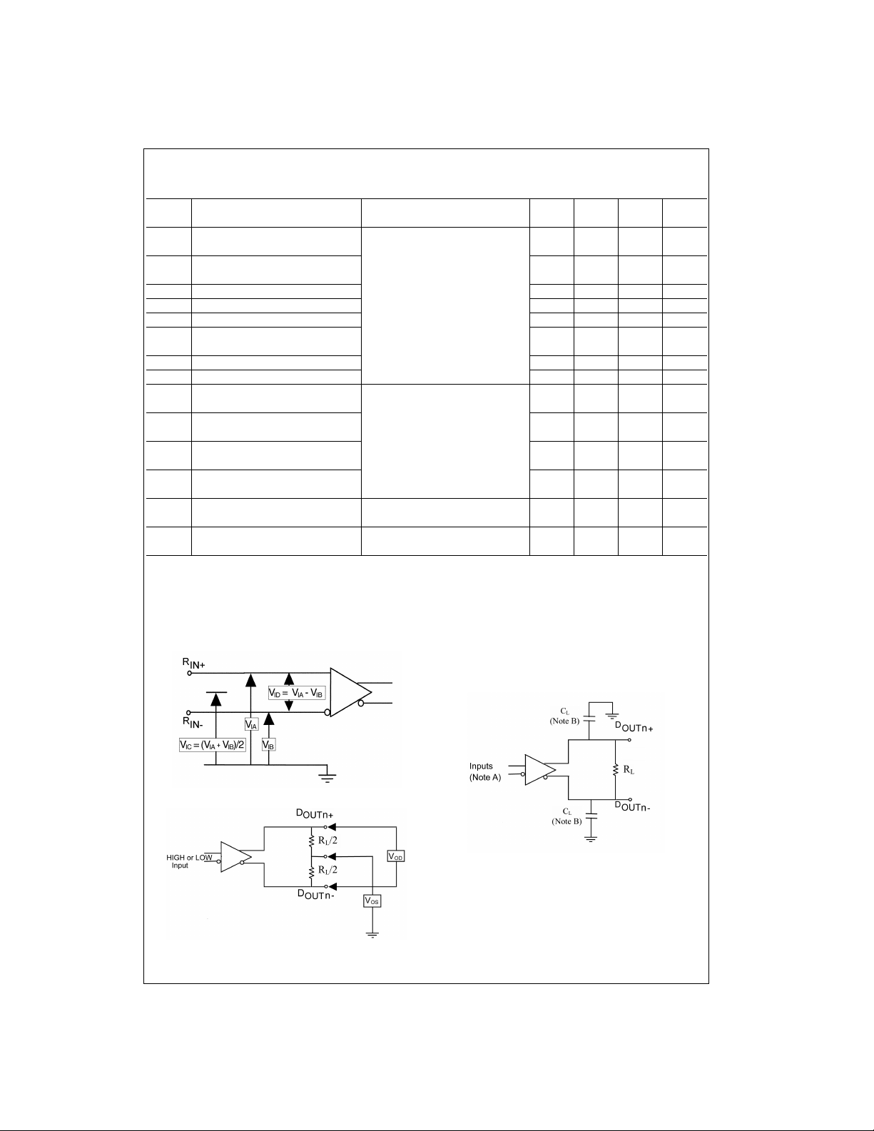
AC Electrical Characteristics
Over supply voltage and operating temperature ranges, unless otherwise specified
Symbol Parameter Test Conditions
t
PLHD
Differential Output Propagation Delay
LOW-to-HIGH
t
PHLD
t
TLHD
t
THLD
t
SK(P)
t
SK(LH)
t
SK(HL)
t
SK(PP)
f
MAX
t
PZHD
Differential Output Propagation Delay
HIGH-to-LOW R
= 100 Ω, CL = 5 pF,
L
Differential Output Rise Time (20% to 80%) VID = 200 mV to 450 mV, 0.29 0.4 0.58 ns
Differential Output Fall Time (80% to 20%) VIC = VID/2 to VCC − (VID/2), 0.29 0.4 0.58 ns
Pulse Skew |t
- t
| Duty Cycle = 50%, 0.02 0.2 ns
PLH
PHL
, Channel-to-Channel Skew See Figure 1 and Figure 1 0.02
(Note 4) 0.02
Part-to-Part Skew (Note 5) 0.5 ns
Maximum Frequency (Note 6)(Note 7) 400 >630 MHz
Differential Output Enable Time
from Z to HIGH
t
PZLD
Differential Output Enable Time
from Z to LOW RL = 100 Ω, CL = 5 pF,
t
PHZD
Differential Output Disable Time See Figure 2 and Figure 3
from HIGH to Z
t
PLZD
Differential Output Disable Time
from LOW to Z
t
DJ
LVDS Data Jitter, VID = 300 mV, PRBS = 223 - 1,
Deterministic VIC = 1.2V at 800 Mbps
t
RJ
LVDS Clock Jitter, VID = 300 mV,
Random (RMS) V
Note 3: All typical values are at TA = 25°C and with VCC = 3.3V.
Note 4: t
tion.
Note 5: t
(either LOW-to-HIGH or HIGH-to-LOW) when both devices operate with the same supply voltage, same temperature, and have identical test circuits.
Note 6: Passing criteria for maximum frequency is the output V
Note 7: Output loading is transmission line environment only; C
, t
SK(LH)
SK(PP)
is the skew between spe cifi ed out puts of a sing le dev ice whe n the ou tput s have iden tical lo ads an d ar e switch ing in the sam e direc-
SK(HL)
is the magnitude of t he difference in propagation delay tim es between any sp ec if ied terminals of two devices switching in the same direction
= 1.2V at 400 MHz
IC
> 250 mV and the duty cycle is better than 45% / 55% with all channels switching.
OD
is < 1 pF of stray test fixture capacitance.
L
Min Typ Max
(Note 3)
0.75 1.1 1.75 ns
0.75 1.1 1.75 ns
0.15 ns
35ns
3.1 5 ns
2.2 5 ns
2.5 5 ns
80 135 ps
1.9 3.5 ps
FIN1108 • FIN1108T (Preliminary)
Units
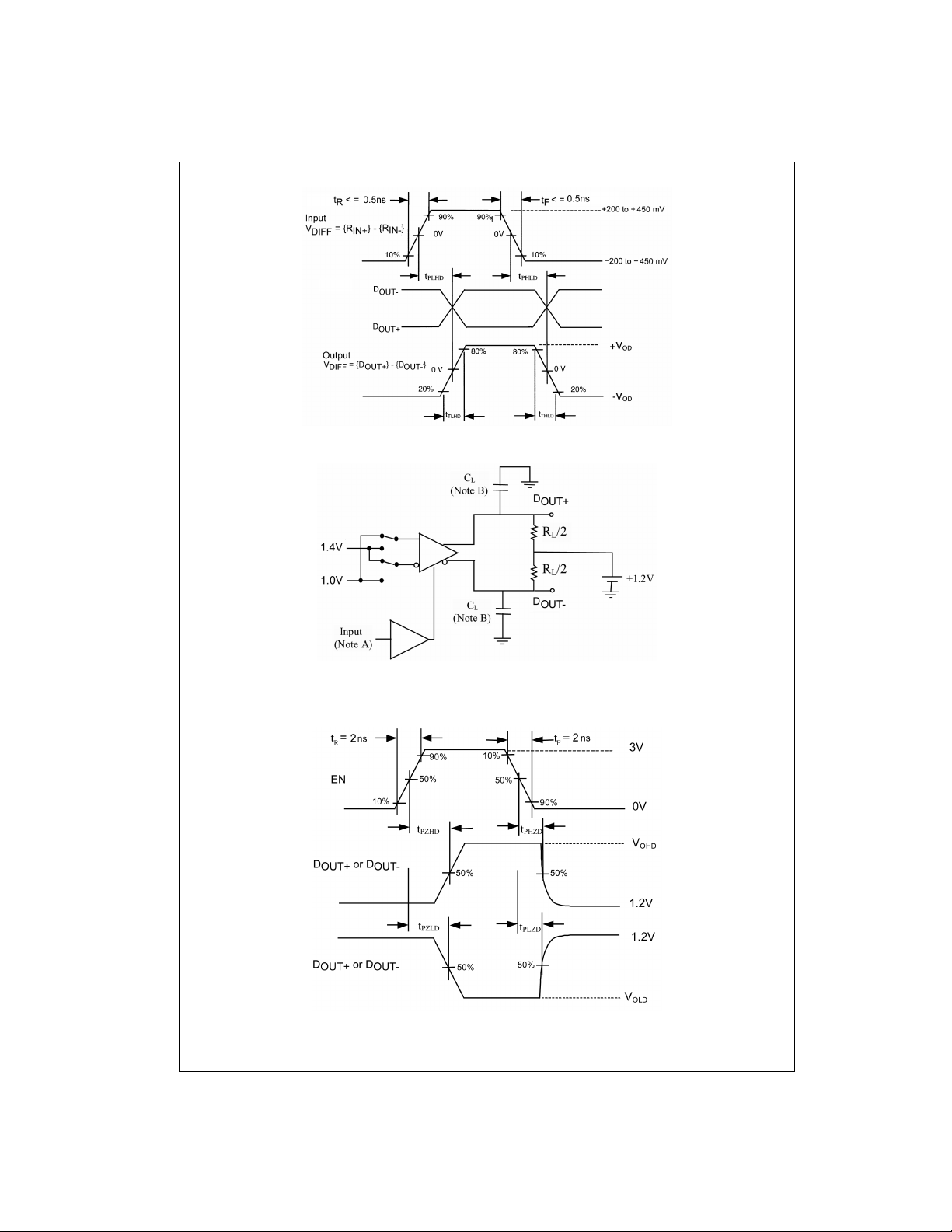
FIGURE 1. Di fferential Receiver Voltage Definitions
FIGURE 2. Differential Driver DC Test Circuit
Note A: All LVDS input pulses hav e f requency = 10 MHz, tR
< = 0.5 ns
or t
F
includes all probe and jig capacitances
Note B: C
L
FIGURE 3. Differential Driver Propagation Delay
and Transition Time Test Circuit
5 www.fairchildsemi.com
Page 6
FIN1108 • FIN1108T (Preliminary)
Note A: All LVTTL input pulses have frequency = 10MHz, tR or tF < = 2 ns
includes all probe an d jig capacitances
Note B: C
L
FIGURE 5. Differential Driver Enable and Disable Circuit
FIGURE 4. AC Waveform
FIGURE 6. Enable and Disable AC Waveforms
www.fairchildsemi.com 6
Page 7
FIN1108 • FIN1108T (Preliminary) LVDS 8 Port High Speed Repeater
48-Lead Thin Shrin k Small Ou tlin e Pack age (TSSOP), JEDEC MO-153, 6.1mm Wide
Fairchild does not assume any responsibility for use of any circuitry described , no circuit patent licenses are implied and
Fairchild reserves the right at any time without notice to change said circuitry and specifications.
LIFE SUPPORT POLICY
FAIRCHILD’S PRODUCTS ARE NOT AUTHORIZED FOR USE AS CRITICAL COMPONENTS IN LIFE SUPPORT
DEVICES OR SYSTEMS WITHOUT THE EXPRESS WRITTEN APPROVAL OF THE PRESIDENT OF FAIRCHILD
SEMICONDUCTOR CORPORATION. As used herein:
1. Life support devices or systems are dev ic es or syste ms
which, (a) are intended for surgical implant into the
body, or (b) support or sustain life, and (c) whose failure
to perform when properly used in accordance with
instructions for use provide d in the l abe ling, can be reasonably expected to result in a significant injury to the
user.
Package Number MTD48
2. A critical componen t in any compo nent o f a life s uppor t
device or system whose failure to perform can be reasonably expected to cause the failure of the life support
device or system, or to affect its safety or effectiveness.
www.fairchildsemi.com
7 www.fairchildsemi.com
 Loading...