

Page 1
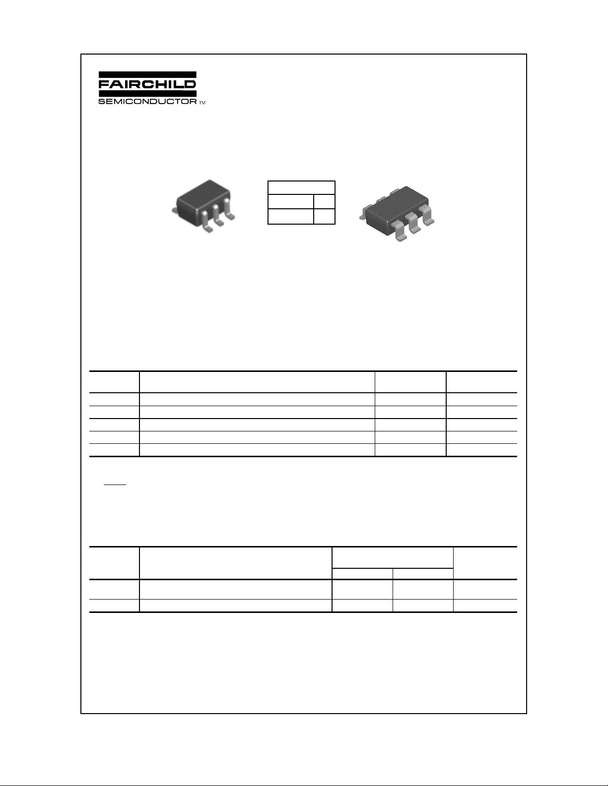
FFB2227A / FMB2227A
FFB2227A
C1
SC70-6
Mark: .AA
Dot denotes pin #1
B2
E2
pin #1
TRANSISTOR TYPE
C1 B1 E1 NPN
C2
B1
E1
C2 B2 E2 PNP
FMB2227A
E1
C1
SuperSOT-6
Mark: .001
Dot denotes pin #1
C2
pin #1
B1
B2
E2
NPN & PNP General Purpose Amplifier
This complementary device is for use as a medium power amplifier and
switch requiring collector currents up to 500 mA. Sourced from Process
19 and 63. See FFB2222A (NPN) and FFB2907A (PNP) for characteristics.
Absolute Maximum Ratings* T
Symbol Parameter Value Units
V
CEO
V
CBO
V
EBO
I
C
TJ, T
stg
*These ratings are limiting values above which the serviceability of any semiconductor device may be impaired.
NOTES:
1) These ratings are based on a maximum junction temperature of 150 degrees C.
2) These are steady state limits. The factory should be consulted on applications involving pulsed or low duty cycle operations.
3) All voltages (V) and currents (A) are negative polarity for PNP transistors.
Collector-Emitter V ol tage 30 V
Collector-Base Voltage 60 V
Emitter-Base Volt age 5.0 V
Collector Current - Continuous 500 mA
Operating and Storage Junction Temperature Range -55 to +150
= 25°C unless otherwise noted
A
C
°
4
Thermal Characteristics T
= 25°C unless otherwise noted
A
Symbol Characteristic Max Units
FFB2227A FMB2227A
P
D
R
JA
θ
1998 Fairchild Semiconductor Corporation
Total Device Dissipation
Derate above 25°C
300
2.4
700
5.6
Thermal Resistance, Junction to Ambient 415 180
mW
mW/°C
C/W
°
Page 2
NPN & PNP General Purpose Amplifier
(continued)
FFB2227A / FMB2227A
Electrical Characteristics T
= 25°C unless otherwise noted
A
Symbol Parameter Test Conditions Min Typ Max Units
OFF CHARACTERISTICS
V
(BR)CEO
V
(BR)CBO
V
(BR)EBO
I
CBO
I
EBO
Collector-Emitter Breakdown
IC = 10 mA, IB = 0 30 V
Voltage*
Collector-Base Breakdown Voltage
Emitter-Base Breakdown Voltage
I
= 10 µA, IE = 0
C
I
= 10 µA, IC = 0
E
Collector Cutoff Current VCB = 50 V, I
Emitter Cutoff Current VEB = 3.0 V, I
60 V
5.0 V
= 0 30 nA
E
= 0 30 nA
C
ON CHARACTERISTICS
h
FE
V
sat
CE(
V
sat
BE(
DC Current Gain IC = 1.0 mA, VCE = 10 V
= 10 mA, VCE = 10 V
I
C
= 150 mA, VCE = 10 V*
I
C
= 300mA, VCE = 10 V*
I
Collector-Emitter S aturation Voltage* IC = 150 mA, IB = 15 mA
)
Base-Emitter Saturation Voltage* IC = 150 mA, IB = 15 mA 1.3 V
)
C
= 300 mA, IB = 30 mA
I
C
50
75
100
30
0.4
1.4
V
V
SMALL SIGNAL CHARACTERISTICS
f
T
C
obo
C
ibo
NF Noise Figure
Current Gain - Bandwidth Product IC = 50 mA, VCE = 20 V,
250 MHz
f = 100 MHz
Output Capacitance VCB = 10 V, IE = 0, f = 100 kHz 4.0 pF
Input Capacitance VEB = 2.0 V, IC = 0, f = 100 kHz 12 pF
I
= 100 µA, V
C
R
= 1.0 kΩ, f = 1.0 kHz
S
CE
= 10 V,
2.0 dB
SWITCHING CHARACTERISTICS
t
on
t
d
t
r
t
off
t
s
t
f
Turn-on Time VCC = 30 V, IC = 150 mA, 30 ns
Delay Time IB1 = 15 mA 8.0 ns
Rise Time 20 ns
Turn-off Time VCC = 6.0 V, IC = 150 mA 80 ns
Storage Time IB1 = IB2 = 15 mA 60 ns
Fall Time 20 ns
*Pulse T est: Pulse Width ≤ 300 µs, Duty Cycle ≤ 2.0%
NOTE: All voltages (V) and currents (A) are negative polarity for PNP transistors.
Page 3

TRADEMARKS
The following are registered and unregistered trademarks Fairchild Semiconductor owns or is authorized to use and is
not intended to be an exhaustive list of all such trademarks.
ACEx™
Bottomless™
CoolFET™
CROSSVOLT™
DOME™
E2CMOS
EnSigna
TM
TM
FACT™
FACT Quiet Series™
FAST
FASTr™
GlobalOptoisolator™
GTO™
HiSeC™
ISOPLANAR™
MICROWIRE™
OPTOLOGIC™
OPTOPLANAR™
P ACMAN™
POP™
PowerTrench
QFET™
QS™
QT Optoelectronics™
Quiet Series™
SILENT SWITCHER
SMART ST ART™
SuperSOT™-3
SuperSOT™-6
SuperSOT™-8
SyncFET™
TinyLogic™
UHC™
VCX™
DISCLAIMER
FAIRCHILD SEMICONDUCTOR RESERVES THE RIGHT TO MAKE CHANGES WITHOUT FURTHER
NOTICE TO ANY PRODUCTS HEREIN T O IMPROVE RELIABILITY , FUNCTION OR DESIGN. FAIRCHILD
DOES NOT ASSUME ANY LIABILITY ARISING OUT OF THE APPLICA TION OR USE OF ANY PRODUCT
OR CIRCUIT DESCRIBED HEREIN; NEITHER DOES IT CONVEY ANY LICENSE UNDER ITS PA TENT
RIGHTS, NOR THE RIGHTS OF OTHERS.
LIFE SUPPORT POLICY
FAIRCHILD’S PRODUCTS ARE NOT AUTHORIZED FOR USE AS CRITICAL COMPONENTS IN LIFE SUPPORT
DEVICES OR SYSTEMS WITHOUT THE EXPRESS WRITTEN APPROVAL OF FAIRCHILD SEMICONDUCTOR CORPORA TION.
As used herein:
1. Life support devices or systems are devices or
systems which, (a) are intended for surgical implant into
the body, or (b) support or sustain life, or (c) whose
failure to perform when properly used in accordance
with instructions for use provided in the labeling, can be
reasonably expected to result in significant injury to the
user.
2. A critical component is any component of a life
support device or system whose failure to perform can
be reasonably expected to cause the failure of the life
support device or system, or to affect its safety or
effectiveness.
PRODUCT STA TUS DEFINITIONS
Definition of Terms
Datasheet Identification Product Status Definition
Advance Information
Preliminary
No Identification Needed
Obsolete
Formative or
In Design
First Production
Full Production
Not In Production
This datasheet contains the design specifications for
product development. Specifications may change in
any manner without notice.
This datasheet contains preliminary data, and
supplementary data will be published at a later date.
Fairchild Semiconductor reserves the right to make
changes at any time without notice in order to improve
design.
This datasheet contains final specifications. Fairchild
Semiconductor reserves the right to make changes at
any time without notice in order to improve design.
This datasheet contains specifications on a product
that has been discontinued by Fairchild semiconductor.
The datasheet is printed for reference information only.
Rev. G
 Loading...