

Page 1
FFA60U60DN
Features
• High v ol tage and high r el ia bi lity
• High speed switching
• Low forward voltage
Applications
• General purpose
• Switc hing mod e po w er supply
• Free-wheeling diode for motor application
• Power switching circuits
1 2 3
ULTRA FAST RECOVERY POWER RECTIFIER
TO-3P
FFA60U60DN
1. Anode 2.Cathode 3. Anod e
Absolute Maximum Ratings
Symbol Parameter Value Units
V
RRM
I
F(AV)
I
FSM
T
J, TSTG
Peak Repetit iv e Reve rse Voltage 600 V
Average Rectified Forward Current @ TC = 100°C60 A
Non-repetitive Peak Surge Current
60Hz Single H a lf- Sine Wave
Operating Junction and Storage Temperature - 65 to +150 °C
(per diode) TC=25°°°°C unless otherwise noted
360 A
Thermal Characteristics
Symbol Parameter Value Units
R
θJC
Electrical C haract eri stics
Symbol Parameter Min. Typ. Max. Units
V
FM
*
I
RM
*
t
rr
I
rr
Q
rr
W
AVL
* Pulse Test: Pulse Width=300µs, Duty Cycle=2%
Maxi mum Ther m al Resis t an ce, Juncti on to Ca se 0.45 °C/W
(per diode) TC=25 °°°°C unless oth erw is e note d
Maximum Instantaneous Forward Voltage
Maximum Instantaneous Reverse Current
Maximum Reverse Recovery Time
Maximum Reverse Recovery Current
Maximum Reverse Recovery Charge
(I
=60A, di/dt = 200A/µs)
F
Avalanche Energy 1.0 - - mJ
= 60A
I
F
I
= 60A
F
@ rated V
= 25 °C
T
C
T
= 100 °C
C
TC = 25 °C
R
T
= 100 °C
C
-
-
-
-
-
-
-
-
-
-
-
-
-
-
2.2
2.0
25
250
90
9
405
V
µA
ns
A
nC
©2000 Fai r ch i ld Semiconductor Inter national
Rev. F, September 2000
Page 2
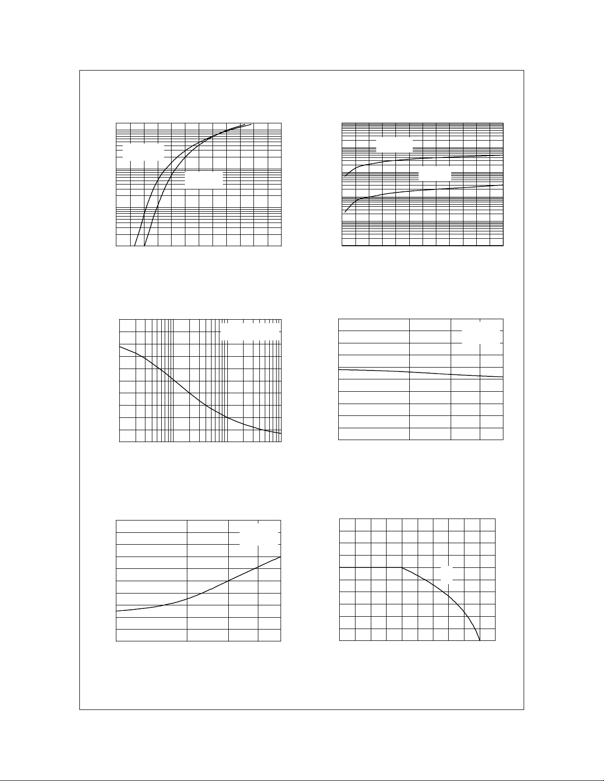
Typical C h aracteristic sTypical C h aracteristic s
FFA60U60DN
100
TC = 100oC
[A]
F
10
TC = 25oC
1
Forward Current , I
0.1
0.0 0.5 1.0 1.5 2.0 2.5 3.0
Forward Voltage , VF [V]
Figure 1. Typical Forward Voltage Drop
vs. Forward Current
1000
900
800
700
600
500
400
300
Capacitance , Cj [pF]
200
100
0.1 1 10 100
Reverse Voltage , VR [V]
Typical Capacitance
at 0V = 850 pF
1000
100
A]
µ
[
R
10
1
0.1
Reverse Current , I
0.01
TC = 100oC
TC = 25oC
100 200 300 400 500 600
Reverse Voltage , VR [V]
Figure 2. Typical Reverse Current
vs. Revers e Voltag e
90
IF = 60A
80
[ns]
rr
70
60
50
Reverse Recovery Time , t
40
100 500
di/dt [A/µs]
TC = 25oC
Figure 3. Typical Junction Capacitance
Figure 4. Typical Reverse Recovery Time
vs. di/dt
20
18
[A]
16
rr
14
12
10
8
6
4
2
Reverse Recovery Current , I
0
100 500
IF = 60A
TC = 25oC
di/dt [A/µs]
Figure 5. Typical Reverse Recovery Current
100
[A]
90
F(AV)
80
70
60
50
40
30
20
10
Average Forward Current , I
0
60 80 100 120 140 160
DC
Case Temperature , TC [oC]
Figure 6. Forward Current Derati ng Curve
vs. di/dt
©2000 Fai r ch i ld Semiconductor Inter national Rev. F, September 2000
Page 3

Package Di men sio n s
ø3.20
±0.10
15.60
13.60
9.60
±0.20
±0.20
±0.20
TO-3P
±0.20
3.80
4.80
1.50
±0.20
+0.15
–0.05
FFA60U60DN
±0.20
13.90
2.00
±0.20
3.00
±0.20
1.00
±0.20
5.45TYP
[5.45
±0.30
±0.20
±0.20
±0.20
12.76
19.90
23.40
±0.20
3.50
±0.30
16.50
5.45TYP
]
[5.45
±0.30
]
±0.20
18.70
1.40
0.60
±0.20
+0.15
–0.05
©2000 Fairchild Semiconductor International
Dimensions in Millimeters
Rev. F, September 2000
Page 4

TRADEMARKS
The following are registered and unregistered trademarks Fairchild Semiconductor owns or is authorized to use and is
not intended to be an exhaustive list of all such trademarks.
ACEx™
Bottomless™
CoolFET™
CROSSVOLT™
DOME™
E2CMOS
EnSigna
TM
TM
FACT™
FACT Quiet Series™
®
FAST
FASTr™
GlobalOptoisolator™
GTO™
HiSeC™
ISOPLANAR™
MICROWIRE™
OPTOLOGIC™
OPTOPLANAR™
POP™
PowerTrench
®
QFET™
QS™
QT Optoelectronics™
Quiet Series™
SuperSOT™-3
SuperSOT™-6
SuperSOT™-8
SyncFET™
TinyLogic™
UHC™
VCX™
DISCLAIMER
FAIRCHILD SEMICONDUCTOR RESERVES THE RIGHT TO MAKE CHANGES WITHOUT FURTHER
NOTICE TO ANY PRODUCTS HEREIN TO IMPROVE RELIABILITY, FUNCTION OR DESIGN. FAIRCHILD
DOES NOT ASSUME ANY LIABILITY ARISING OUT OF THE APPLICATION OR USE OF ANY PRODUCT
OR CIRCUIT DESCRIBED HEREIN; NEITHER DOES IT CONVEY ANY LICENSE UNDER ITS PATENT
RIGHTS, NOR THE RIGHTS OF OTHERS.
LIFE SUPPORT POLICY
FAIRCHILD’S PRODUCTS ARE NOT AUTHORIZED FOR USE AS CRITICAL COMPONENTS IN LIFE SUPPORT
DEVICES OR SYSTEMS WITHOUT THE EXPRESS WRITTEN APPROVAL OF FAIRCHILD SEMICONDUCTOR CORPORATION.
As used herein:
1. Life support devices or systems are devices or
systems which, (a) are intended for surgical implant into
the body, or (b) support or sustain life, or (c) whose
failure to perform when properly used in accordance
with instructions for use provided in the labeling, can be
reasonably expected to result in significant injury to the
user.
2. A critical component is any component of a life
support device or system whose failure to perform can
be reasonably expected to cause the failure of the life
support device or system, or to affect its safety or
effectiveness.
PRODUCT STATUS DEFINITIONS
Definition of Terms
Datasheet Identification Product Status Definition
Advance Information
Preliminary
No Identification Needed
Obsolete
Formative or
In Design
First Production
Full Production
Not In Production
This datasheet contains the design specifications for
product development. Specifications may change in
any manner without notice.
This datasheet contains preliminary data, and
supplementary data will be published at a later date.
Fairchild Semiconductor reserves the right to make
changes at any time without notice in order to improve
design.
This datasheet contains final specifications. Fairchild
Semiconductor reserves the right to make changes at
any time without notice in order to improve design.
This datasheet contains specifications on a product
that has been discontinued by Fairchild semiconductor.
The datasheet is printed for reference information only.
Rev. F1
 Loading...