

Page 1

User Guide for
FEBL010
Evaluation Board
Universal LED Driver using the FL6961
CRM PFC Controller
Featured Fairchild Product:
FL6961
Direct questions or comments
about this evaluation board to:
“Worldwide Direct Support”
Fairchild Semiconductor.com
© 2012 Fairchild Semiconductor Corporation 1 FEB-L010_FL6961 • Rev. 1.0.0
Page 2

Table of Contents
1. Introduction ............................................................................................................................... 3
1.1. General Description of FL6961 ....................................................................................... 3
1.2. Features of FL6961 .......................................................................................................... 3
1.3. Block Diagram ................................................................................................................. 4
2. General Specifications for Evaluation Board ........................................................................... 5
2.1 Photographs of the Evaluation Board .............................................................................. 6
2.2 Printed Circuit Board ....................................................................................................... 7
2.3 Schematic of the Evaluation Board .................................................................................. 8
2.4 Bill of Materials ............................................................................................................... 9
2.5 Connections Transformer and Winding Specifications ................................................. 11
3 Performance of Evaluation Board ........................................................................................... 12
3.1 Test Condition & Items .................................................................................................. 12
3.2 Electrical Efficiency ....................................................................................................... 13
3.3 Power Factor .................................................................................................................. 14
3.4 Constant Current & Constant Voltage (CC/CV) ........................................................... 15
3.5 THD Performance .......................................................................................................... 17
3.6 Temperature Checking Results ...................................................................................... 19
3.7 Startup Time................................................................................................................... 20
3.8 Operation Waveforms .................................................................................................... 22
3.9 Short-Circuit Protection ................................................................................................. 24
3.10 Stress of the MOSFET & Rectifier ................................................................................ 25
3.11 Stress of the MOSFET & Rectifier ................................................................................ 29
4. Revision History ..................................................................................................................... 30
© 2012 Fairchild Semiconductor Corporation 2 FEB-L010_FL6961 • Rev. 1.0.0
Page 3

This user guide supports the evaluation kit for the FL6961. It should be used in
conjunction with the FL6961 datasheet as well as Fairchild’s application notes and
technical support team. Please visit Fairchild’s website at www.fairchildsemi.com.
1. Introduction
This document describes the proposed solution for a universal LED ballast using the
FL6961 CRM PFC controller. The input voltage range is 90V
one DC output with a constant current of 1.25A at 24V
general description of FL6961, the power supply specification, schematic, bill of
materials, and the typical operating characteristics.
1.1. General Description of FL6961
The FL6961 is an active Power Factor Correction (PFC) controller for boost PFC
applications that operate in Critical conduction Mode (CRM). It uses a voltage mode
PWM that compares an internal ramp signal with the error amplifier output to generate
the MOSFET turn-off signal. Because the voltage-mode CRM PFC controller does not
need rectified AC line voltage information, it saves the power loss of the input voltagesensing network required by the current-mode CRM PFC controller.
1.2. Features of FL6961
– 265V
RMS
. This document contains
MAX
and there is
RMS
Boundary Mode PFC Controller
Low Input Current THD
Controlled On-Time PWM
Zero-Current Detection (ZDC)
Cycle-by-Cycle Current Limiting
Leading-Edge Blanking Instead of RC Filtering
Low Startup Current: 10µA (Typical)
Low Operating Current: 4.5mA (Typical)
Feedback Open-Loop Protection
Programmable Maximum On-Time (MOT)
Output Over-Voltage Clamping Protection
Clamped Gate Output Voltage: 16.5V
© 2012 Fairchild Semiconductor Corporation 3 FEB-L010_FL6961 • Rev. 1.0.0
Page 4
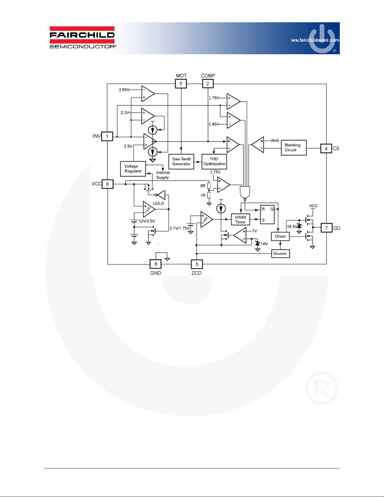
1.3. Block Diagram
Figure 1. Internal Block Diagram of FL6961
© 2012 Fairchild Semiconductor Corporation 4 FEB-L010_FL6961 • Rev. 1.0.0
Page 5

2. General Specifications for Evaluation Board
All data of the evaluation board was measured with the board enclosed in a case and
external temperature of around 25°C.
Table 1. Summary of Features and Performance
Main Controller FL6961
Input Voltage Range 90VAC~265VAC
Input Voltage Frequency 47Hz~63Hz
Rated Output Power 30W
Rated Output Voltage 24V
Rated Output Current 1.25A
Application LED Lighting
© 2012 Fairchild Semiconductor Corporation 5 FEB-L010_FL6961 • Rev. 1.0.0
Page 6
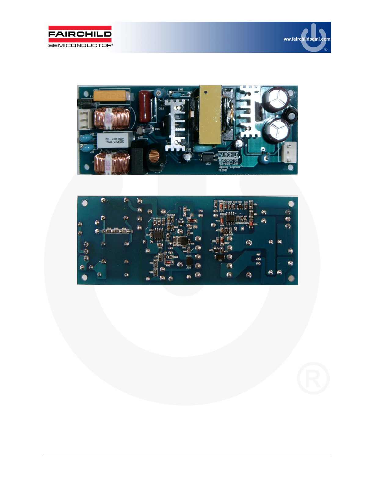
2.1 Photographs of the Evaluation Board
Figure 2. Photograph (125mm (W) x 41mm (H)) Top View
Figure 3. Photograph (125mm (W) x 41mm (H)) Bottom View
© 2012 Fairchild Semiconductor Corporation 6 FEB-L010_FL6961 • Rev. 1.0.0
Page 7
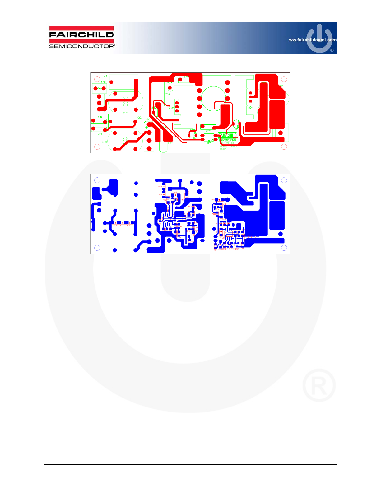
2.2 Printed Circuit Board
Figure 4. Printed PCB, Top Side
Figure 5. Printed PCB, Bottom Side
© 2012 Fairchild Semiconductor Corporation 7 FEB-L010_FL6961 • Rev. 1.0.0
Page 8
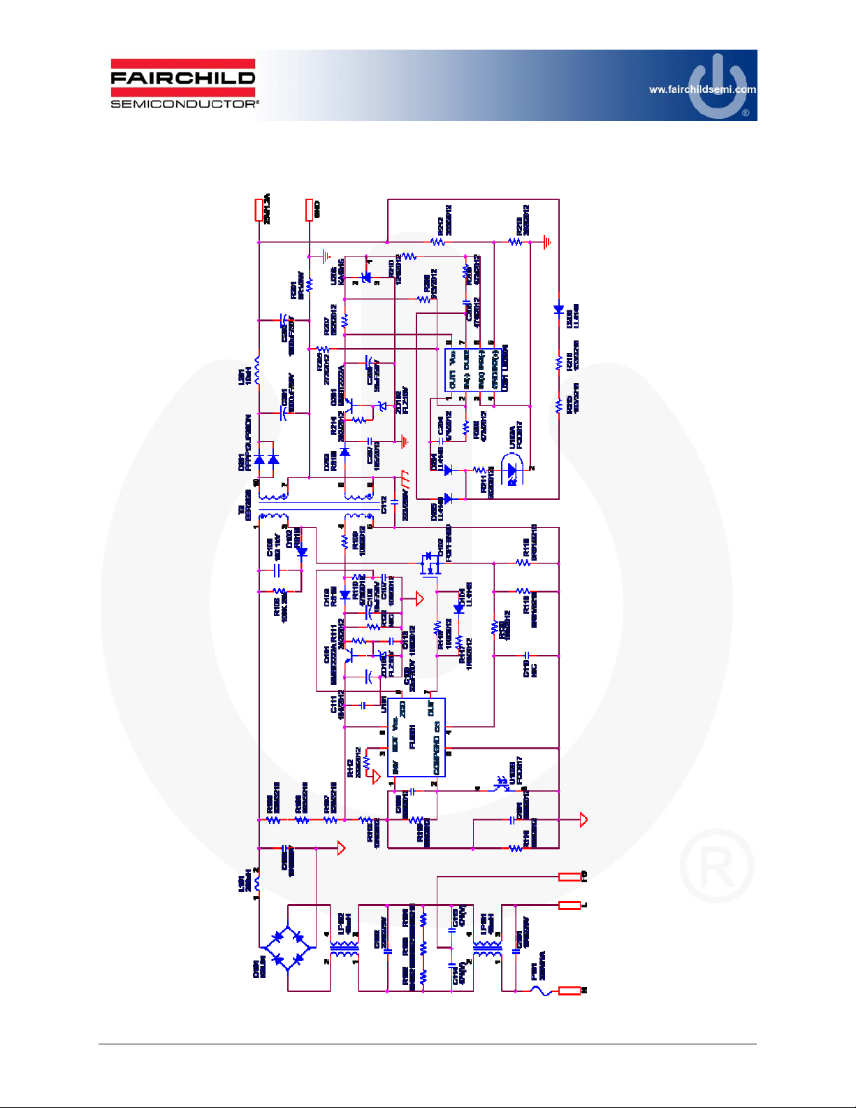
2.3 Schematic of the Evaluation Board
Figure 6. Schematic of Evaluation
© 2012 Fairchild Semiconductor Corporation 8 FEB-L010_FL6961 • Rev. 1.0.0
Page 9
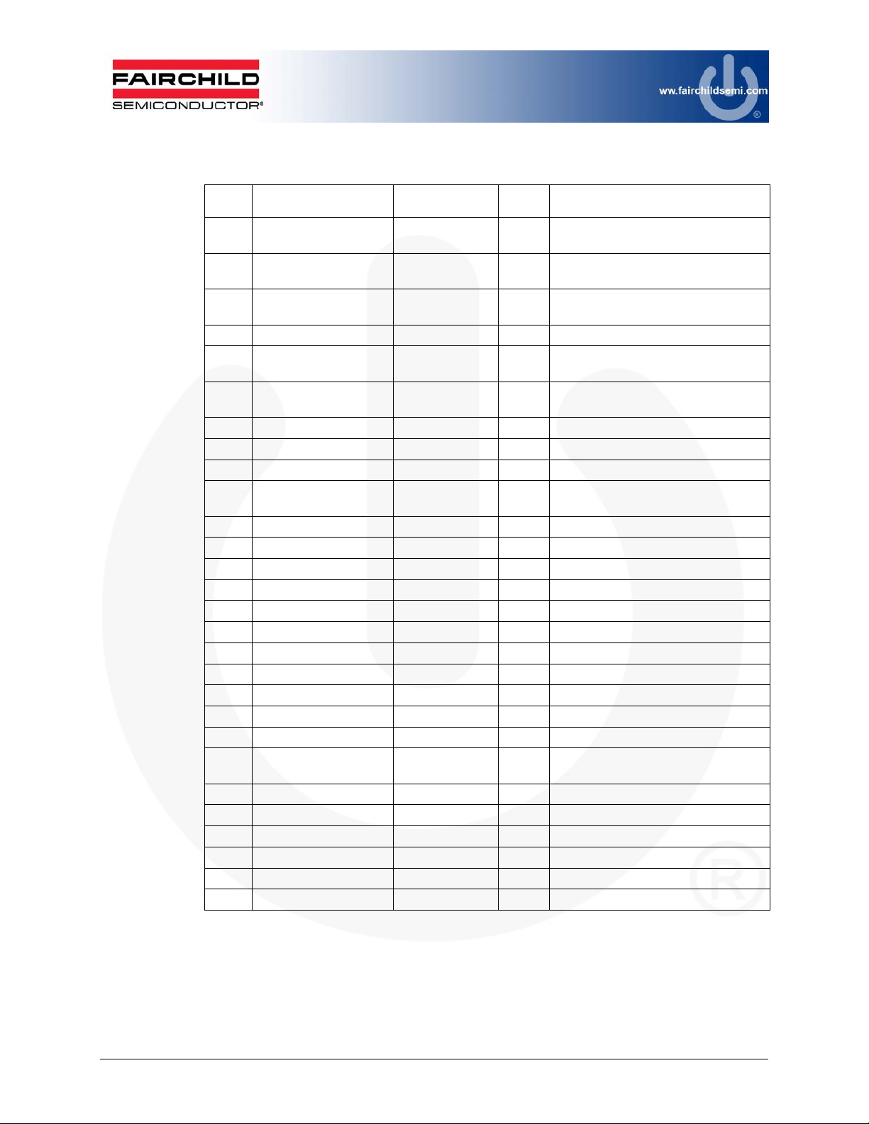
2.4 Bill of Materials
Table 2. Bill of Materials of Evaluation Board
Item
No.
1 U101 FL6961 1
2 D102, D103 ,D203 RS1M 3
3 Q102 FQPF8N80C 1
4 D101 KBL04 1 Bridge Diode (Fairchild Product)
5
6 Q101, Q201 MMBT2222A 2
7 U102 FOD817 1 Opto-Coupler (Fairchild Product)
8 U203 KA431S 1 Shunt Regulator (Fairchild Product)
9 U201 LM2904 1 Dual OP Amp (Fairchild Product)
10 D201 FFPF12UP20DN 1
11 ZD101, ZD102 FLZ16V 2 Zener Diode (Fairchild Product)
12 C106 102/1kV 1 Ceramic-Capacitor
13 C101 154/275V 1 X – Capacitor
14 C102 224/275V 1 X – Capacitor
15 C112 222/250V 1 Y – Capacitor
16 C114, C115 471/250V 2 Y – Capacitor
17 C201, C202 1000µF / 35V 2 Electrolytic Capacitor
18 C108 10µF/50V 1 Electrolytic Capacitor
19 C109 22µF/50V 1 Electrolytic Capacitor
20 C203 33µF/50V 1 Electrolytic Capacitor
21 C103 154/630V 1 Film Capacitor
22
23 C107 100/2012 1 SMD Capacitor 2012
24 C110 N/C 1 SMD Capacitor 2012
25 C111 104/2012 1 SMD Capacitor 2012
26 C204, C205 474/2012 2 SMD Capacitor 2012
27 F101 250V/1A 1 Fuse
28 L101 200µH 1 Inductor
Part Reference Value Qty Description (Manufacturer)
D104, D204, D205,
D206
C104, C105, C113,
C207
CRM PFC Controller
(Fairchild Product)
1000V/1A Ultra-Fast Recovery Diode
(Fairchild Product)
800V/8A MOSFET
(Fairchild Product)
LL4148 4
105/2012 4 SMD Capacitor 2012
General-Purpose Diode
(Fairchild Product)
General-Purpose Transistor
(Fairchild Product)
Ultrafast Recovery Power Rectifier
(Fairchild Product)
Continued on the following page…
© 2012 Fairchild Semiconductor Corporation 9 FEB-L010_FL6961 • Rev. 1.0.0
Page 10
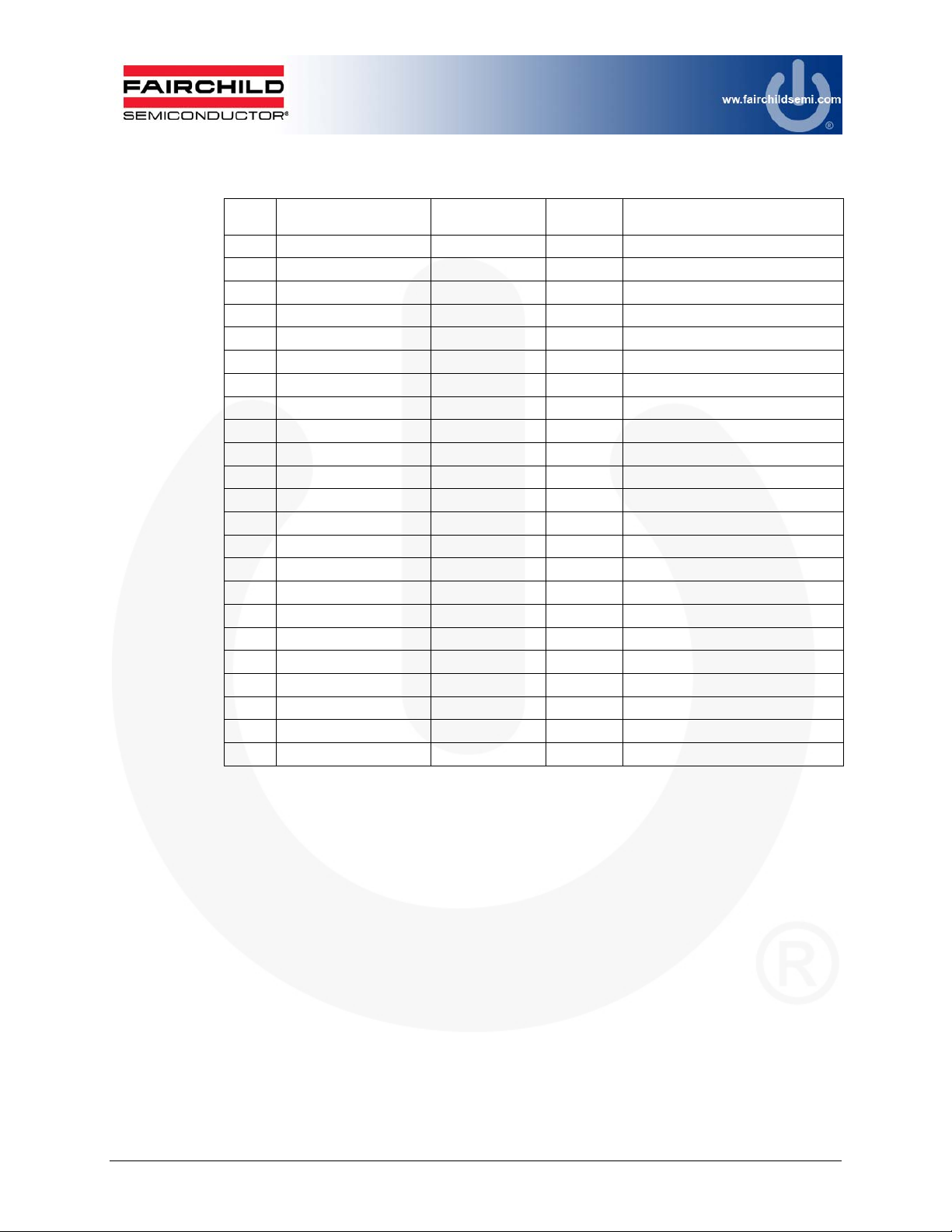
Bill of Materials (Continued)
Item
No.
29 LF101, LF102 40mH 2 Line Filter
30 L201 10µH 1 Stick Inductor
31 T2 EER2828 1 Transformer, 700µH, 1kHz, 1V
32 R201 0R1/3W 1 Metal Film Resistor 3W
33 R108 100K 2W 1 Metal Oxide Film Resistor 2W
34 R122 N/C 1 SMD Resistor 2012
35 R109, R116, R120 100/2012 3 SMD Resistor 2012
36 R110, R208, R209 473/2012 3 SMD Resistor 2012
37 R111, R213, R214 392/2012 3 SMD Resistor 2012
38 R112, R212 333/2012 2 SMD Resistor 2012
39 R113, R210 124/2012 2 SMD Resistor 2012
40 R114 103/2012 1 SMD Resistor 2012
41 R115 203/2012 1 SMD Resistor 2012
42 R117 1R0/2012 1 SMD Resistor 2012
43 R205 272/2012 1 SMD Resistor 2012
44 R206 513/2012 1 SMD Resistor 2012
45 R207 682/2012 1 SMD Resistor 2012
46 R211 562/2012 1 SMD Resistor 2012
47 R102, R103, R104 564/3216 3 SMD Resistor 3216
48 R105, R106, R107 823/3216 3 SMD Resistor 3216
49 R118, R119 0R51/3216 2 SMD Resistor 3216
50 R215 103/3216 1 SMD Resistor 3216
51 R216 153/3216 1 SMD Resistor 3216
Part Reference Value Qty Description (Manufacturer)
© 2012 Fairchild Semiconductor Corporation 10 FEB-L010_FL6961 • Rev. 1.0.0
Page 11
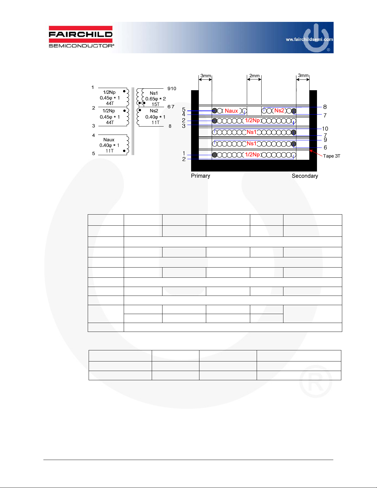
2.5 Connections Transformer and Winding Specifications
Figure 7. Transformer Specifications & Construction [EER2828]
Table 3. Winding Specifications
No Winding Pin (S F) Wire Turns Winding Method
1 1/2Np 1 2 0.45φ×1 44 Ts Solenoid Winding
2 Insulation: Polyester Tape t = 0.025mm, 3-Layer
3 Ns1 6 9 0.65φ×2 15 Ts Solenoid Winding
4 Insulation: Polyester Tape t = 0.025mm, 3-Layer
5 Ns1 7 10 0.65φ×2 15 Ts Solenoid Winding
6 Insulation: Polyester Tape t = 0.025mm, 3Layers
7 1/2Np 2 3 0.45φ×1 44 Ts Solenoid Winding
8 Insulation: Polyester Tape t = 0.025mm, 3-Layer
9
10 Insulation: Polyester Tape t = 0.025mm, 3-Layer
Table 4. Electrical Characteristics
Pin Specifications Remark
Inductance 1 – 3 700µH ±7% 1kHz, 1V
Leakage 1 – 3 30µH Maximum Short All Output Pins
Naux 5 4 0.45φ×1 11 Ts
Ns1 7 8 0.45φ×1 11 Ts
Solenoid Winding
© 2012 Fairchild Semiconductor Corporation 11 FEB-L010_FL6961 • Rev. 1.0.0
Page 12

3 Performance of Evaluation Board
3.1 Test Condition & Items
Table 5. Test Condition & Test Equipment
Ambient Temperature T
Test Equipment
Test Items
= 25°C
A
AC Power Source: PCR500L by Kikusui
Power Analyzer: 2574R series by Xitron
Electronic Load: PLZ303WH by KIKUSUI
Multi Meter: 2002 by KEITHLEY, 45 by FLUKE
Oscilloscope: 104Xi by LeCroy
EMI Test Receiver: ESCS30 by ROHDE & SCHWARZ
Two-Line V-Network: ENV216 by ROHDE & SCHWARZ
Thermometer: Thermal CAM SC640 by FLIR SYSTEMS
3.2. Electrical Efficiency
3.3. Power Factor
3.4. Constant Current & Constant Voltage (CC/CV)
3.5. THD Performance
3.6. Temperature Checking Results
3.7. Startup Time
3.8. Operation Waveforms
3.9 Short-Circuit Protection
3.10. Stress on MOSFET & Rectifier
3.11. EMI Result
© 2012 Fairchild Semiconductor Corporation 12 FEB-L010_FL6961 • Rev. 1.0.0
Page 13
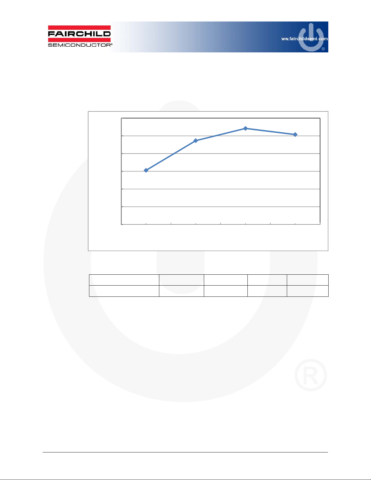
3.2 Electrical Efficiency
Figure 8 shows at least 84% system efficiency with universal input condition at the rated
output load.
87.0
86.0
85.0
84.0
83.0
Efficiency [%]
82.0
81.0
90V 115V 230 265V
Input Voltage [VAC]
Figure 8. System Efficiency
Input Voltage 90VAC 115VAC 230VAC 265VAC
Efficiency [%] 84.05 85.73 86.42 86.07
© 2012 Fairchild Semiconductor Corporation 13 FEB-L010_FL6961 • Rev. 1.0.0
Page 14
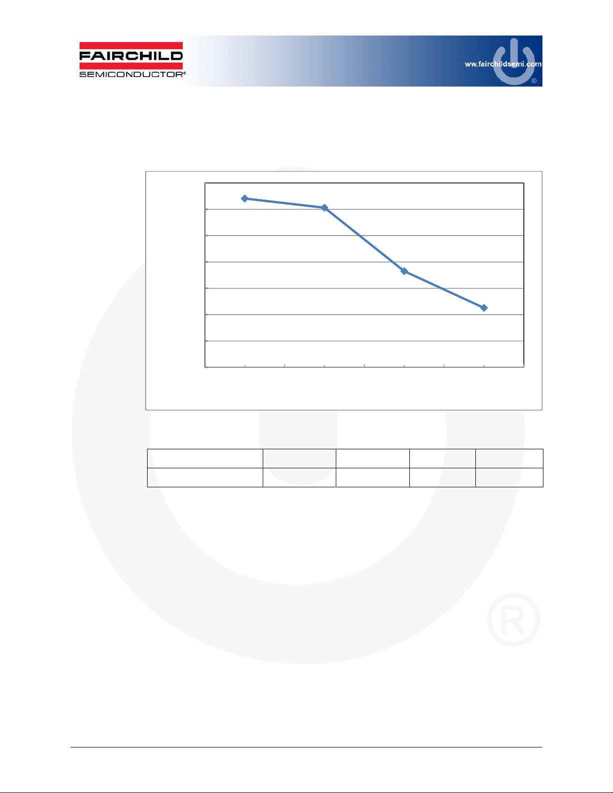
3.3 Power Factor
Figure 9 shows over 90% PF results with universal input condition at rated output power.
1.00
0.98
0.96
0.94
0.92
Power Factor
0.90
0.88
0.86
90V 115V 230 265V
Input Voltage [VAC]
Figure 9. Power Factor
Input Voltage 90VAC 115VAC 230VAC 265VAC
PF 0.9882 0.9812 0.9330 0.9051
© 2012 Fairchild Semiconductor Corporation 14 FEB-L010_FL6961 • Rev. 1.0.0
Page 15
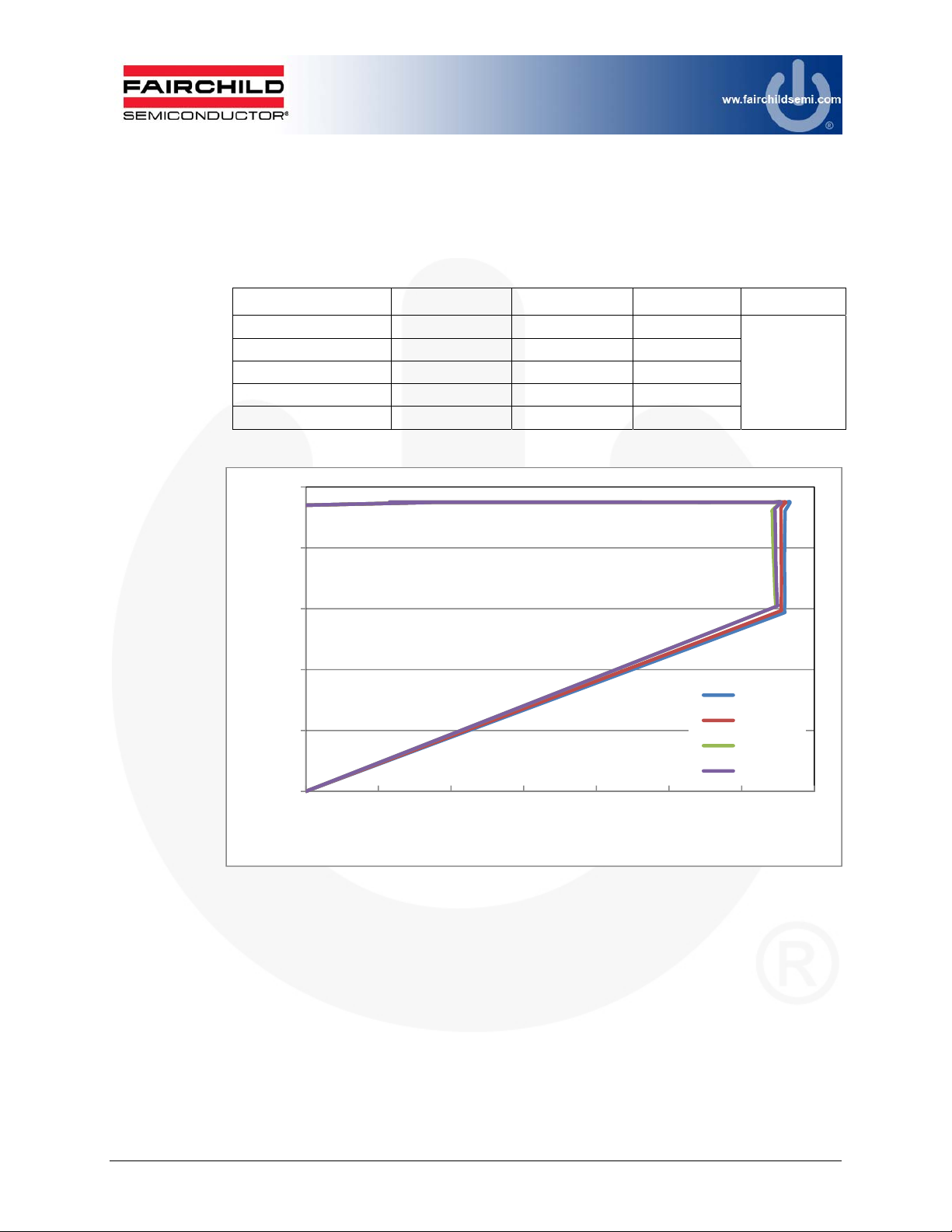
3.4 Constant Current & Constant Voltage (CC/CV)
Figure 10 shows the typical CC/CV performance on the board, showing very stable CC
performance at 90V
Input Voltage Min. Current Max. Current Tolerance Remark
90VAC / 60Hz 1.318 1.333 1.13%
115VAC / 60Hz 1.308 1.321 0.98%
230VAC / 60Hz 1.285 1.307 1.68%
230VAC / 60Hz 1.292 1.308 1.22%
Total 1.285 1.333 3.60%
25
20
~ 265VAC input conditions.
AC
< 10%
15
10
Output Voltage[V]
5
0
0.0 0.2 0.4 0.6 0.8 1.0 1.2 1.4
Output Current [A]
Figure 10. CC/CV Performance
90Vac
115Vac
230Vac
265Vac
© 2012 Fairchild Semiconductor Corporation 15 FEB-L010_FL6961 • Rev. 1.0.0
Page 16
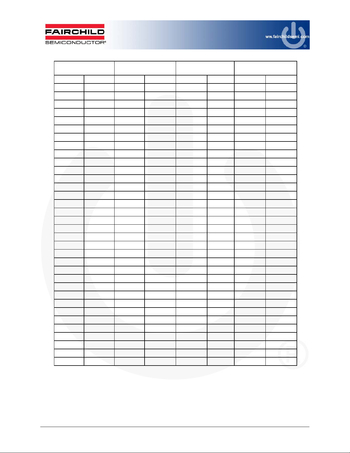
Table 6. CC and CV Measured Data
90V
AC
115V
AC
220V
AC
265V
AC
Vout Iout V out Iout Vout Iout Vout Iout
23.50 0.0000 23.50 0.0000 23.50 0.0000 23.50 0.0000
23.75 0.2440 23.75 0.2440 23.75 0.2440 23.74 0.2440
23.75 0.2813 23.75 0.2810 23.75 0.2810 23.74 0.2810
23.75 0.3190 23.75 0.3190 23.75 0.3190 23.74 0.3190
23.75 0.3630 23.75 0.3630 23.75 0.3630 23.74 0.3630
23.75 0.4320 23.75 0.4320 23.75 0.4320 23.74 0.4317
23.75 0.5260 23.75 0.5260 23.75 0.5260 23.74 0.5260
23.74 0.6760 23.75 0.6760 23.75 0.6760 23.74 0.6760
23.74 0.9520 23.75 0.9520 23.75 0.9520 23.74 0.9520
23.74 1.2140 23.75 1.2140 23.75 1.2140 23.74 1.2140
23.74 1.2770 23.75 1.2770 23.75 1.2770 23.74 1.2770
23.74 1.3080 23.75 1.3080 23.75 1.3067 23.74 1.3080
23.74 1.3330 23.32 1.3210 22.88 1.2847 23.00 1.2920
22.85 1.3197 22.67 1.3090 22.26 1.2850 22.38 1.2923
22.34 1.3190 22.16 1.3090 21.77 1.2853 21.88 1.2923
21.75 1.3190 21.59 1.3090 21.21 1.2857 21.32 1.2930
21.28 1.3187 21.13 1.3090 20.76 1.2863 20.87 1.2930
20.75 1.3183 20.60 1.3090 20.25 1.2867 20.35 1.2930
20.16 1.3183 20.02 1.3090 19.69 1.2873 19.78 1.2937
19.68 1.3180 19.55 1.3093 19.24 1.2880 19.32 1.2937
19.15 1.3180 19.03 1.3093 18.73 1.2887 18.81 1.2940
18.65 1.3180 18.54 1.3097 18.25 1.2893 18.32 1.2947
18.11 1.3180 18.00 1.3097 17.73 1.2903 17.79 1.2947
17.60 1.3183 17.49 1.3097 17.24 1.2907 17.30 1.2953
17.07 1.3183 16.96 1.3100 16.72 1.2913 16.78 1.2960
16.45 1.3190 16.34 1.3097 16.12 1.2923 16.18 1.2970
15.98 1.3190 15.87 1.3093 15.70 1.2930 15.75 1.2977
15.70 1.3190 15.59 1.3093 15.41 1.2940 15.45 1.2980
15.46 1.3190 15.35 1.3093 15.18 1.2947 15.22 1.2983
15.18 1.3183 15.07 1.3093 0.00 0.0000 0.00 0.0000
14.95 1.3180 14.84 1.3087 0.00 0.0000
14.81 1.3180 0.00 0.0000 0.00 0.0000
14.68 1.3180 0.00 0.0000 0.00 0.0000
0.00 0.0000 0.00 0.0000 0.00 0.0000
© 2012 Fairchild Semiconductor Corporation 16 FEB-L010_FL6961 • Rev. 1.0.0
Page 17
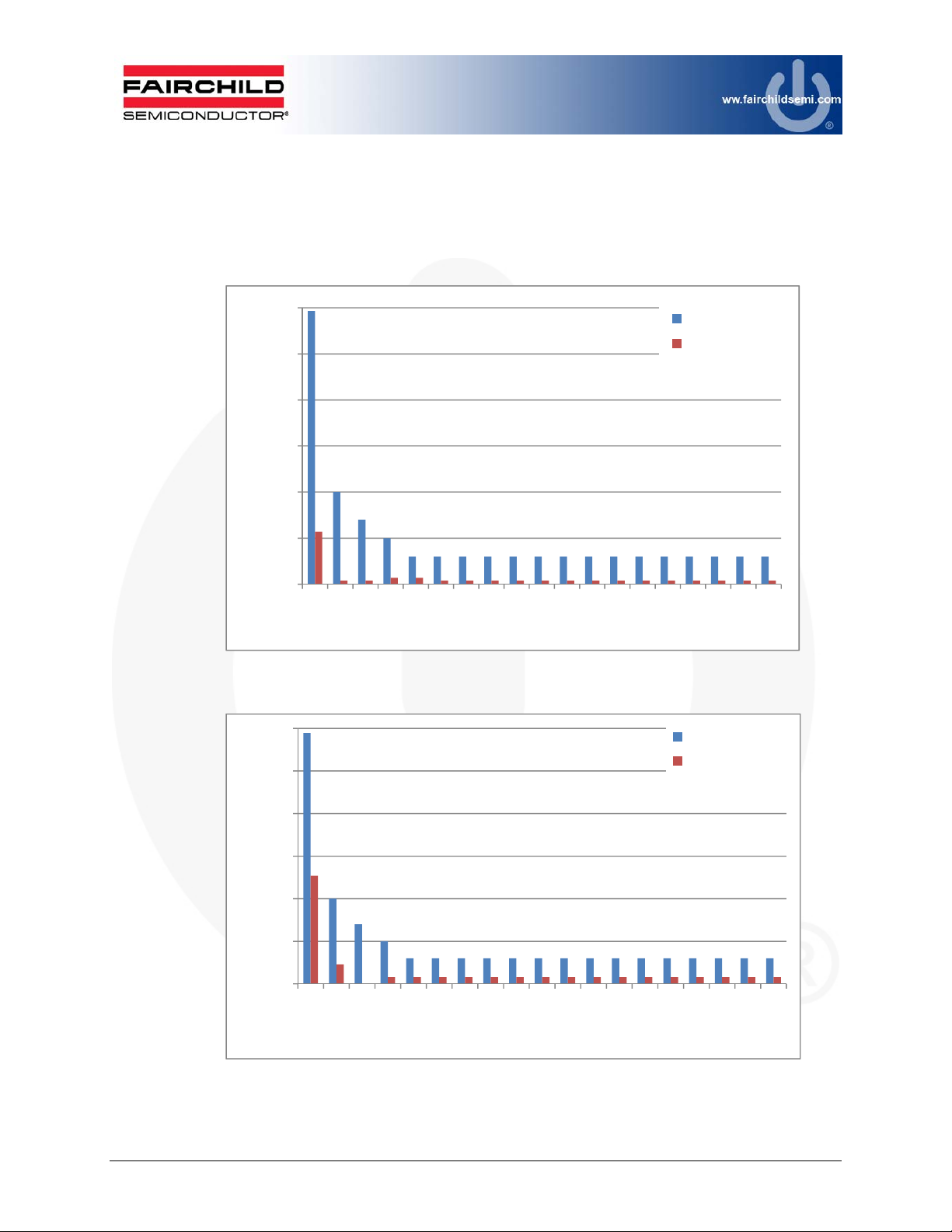
3.5 THD Performance
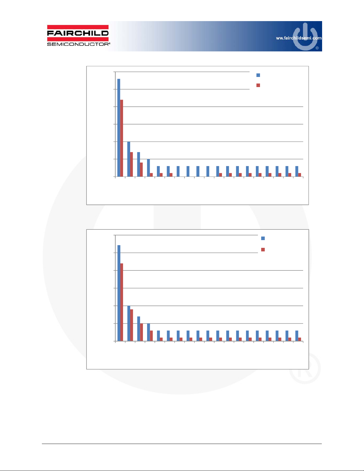
Figure 11 through Figure 14 show the test results of the FL6961 evalutaiton board. All of
the results meet international regulations.
30
25
20
15
10
% of Fundamental
5
0
3 5 7 9 11 13 15 17 19 21 23 25 27 29 31 33 35 37 39
30
25
Harmonic Number
Figure 11. THD Performance Results at 90VAC
90Vac(IEC)
90Vac(Test)
115Vac(IEC)
115Vac(Test)
20
15
10
% of Fundamental
5
0
3 5 7 9 11 13 15 17 19 21 23 25 27 29 31 33 35 37 39
Harmonic Number
Figure 12. THD Performance Results at 115VAC
© 2012 Fairchild Semiconductor Corporation 17 FEB-L010_FL6961 • Rev. 1.0.0
Page 18
30
25
20
15
10
% of Fundamental
5
0
3 5 7 9 11 13 15 17 19 21 23 25 27 29 31 33 35 37 39
Figure 13. THD Performance Results at 230VAC
30
230Vac(IEC)
230Vac(Test)
Harmonic Number
265Vac(IEC)
25
265Vac(Test)
20
15
10
% of Fundamental
5
0
3 5 7 9 11 13 15 17 19 21 23 25 27 29 31 33 35 37 39
Harmonic Number
Figure 14. THD Performance Results at 265VAC
© 2012 Fairchild Semiconductor Corporation 18 FEB-L010_FL6961 • Rev. 1.0.0
Page 19
3.6 Temperature Checking Results
(
(
(
)
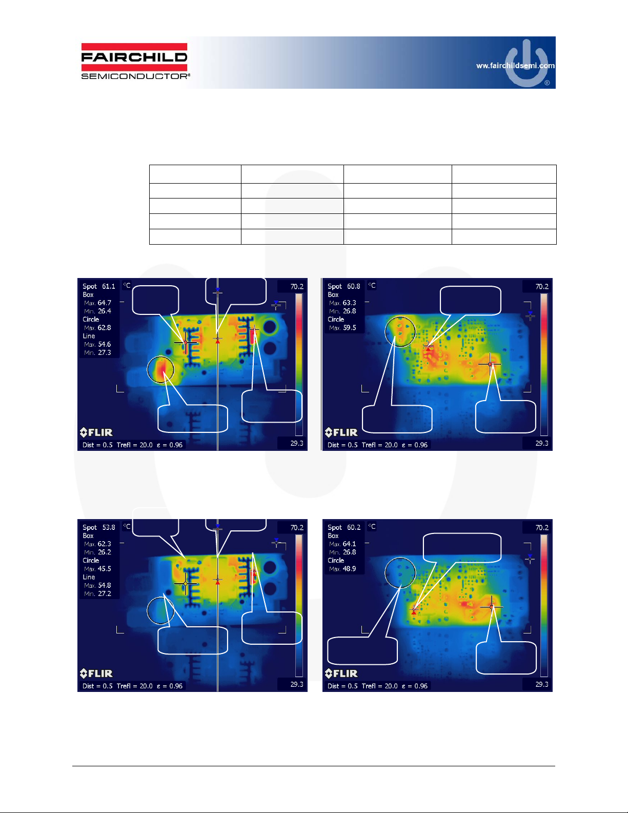
Figure 15 through Figure 18 show the temperature-checking results on the board in
minimum and maximum input voltage condition.
90VAC / 60Hz 265VAC / 60Hz Remark
Bridge Diode 62.8°C 53.8°C Top Side Circle
Transformer 54.6°C 54.8°C Top Side Line
FET 61.1°C 53.8°C Top Side Spot
Rectifier 64.7°C 62.3°C Top Side Box
FET
(61.1℃)
Bridge Diode
62.8℃)
Transformer
(54.6°C)
Rectifier
(64.7°C)
Bridge Diode
(59.5)
FET
(63.3℃)
Rectifier
(60.8°C)
Figure 15. 90VAC / 60Hz; Top Side Figure 16. 90VAC / 60Hz; Bottom Side
FET
(53.8℃)
Transformer
(54.8℃)
Start Up Resistor
(64.1℃)
Rectifier
Bridge Diode
45.5℃)
(62.3℃)
Bridge Diode
48.9℃
Rectifier
(60.2℃)
Figure 17. 265VAC / 60Hz; Top Side Figure 18. 265VAC / 60Hz; Bottom Side
© 2012 Fairchild Semiconductor Corporation 19 FEB-L010_FL6961 • Rev. 1.0.0
Page 20
3.7 Startup Time
V
VAC/
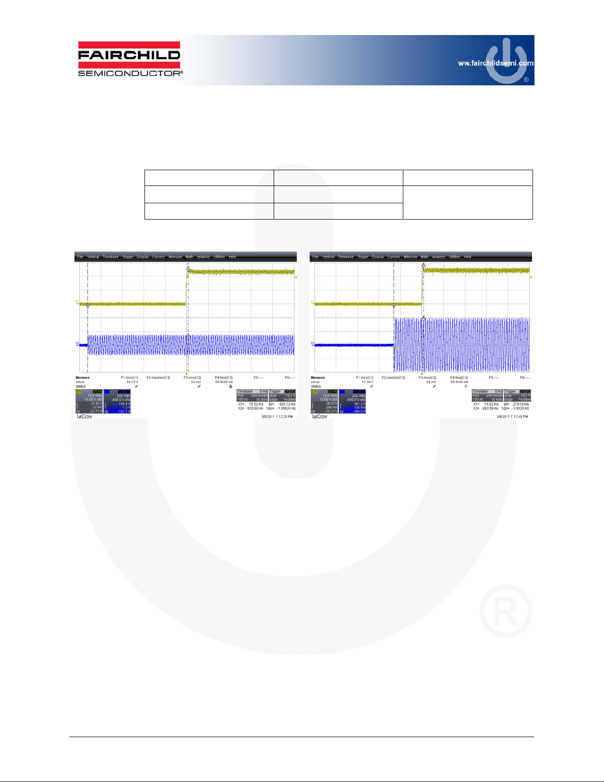
Figure 19 and Figure 20 show the typical startup performance of the board. A longer
startup time to release the UVLO function can be achieved at 90V
265V
the board.
condition. This time normally depends on the starting resistor and capacitor on
AC
Input Voltage Turn-On Time Remark
90VAC / 60Hz 0.936s
265VAC / 60Hz 0.279s
condition rather than
AC
< 1s
Figure 19. 90
/ 60Hz CH1 (Yellow): V
AC
CH3 (Blue): V
IN
OUT
,
Figure 20. 265
60Hz CH1 (Yellow): V
CH3 (Blue): V
IN
OUT
,
© 2012 Fairchild Semiconductor Corporation 20 FEB-L010_FL6961 • Rev. 1.0.0
Page 21
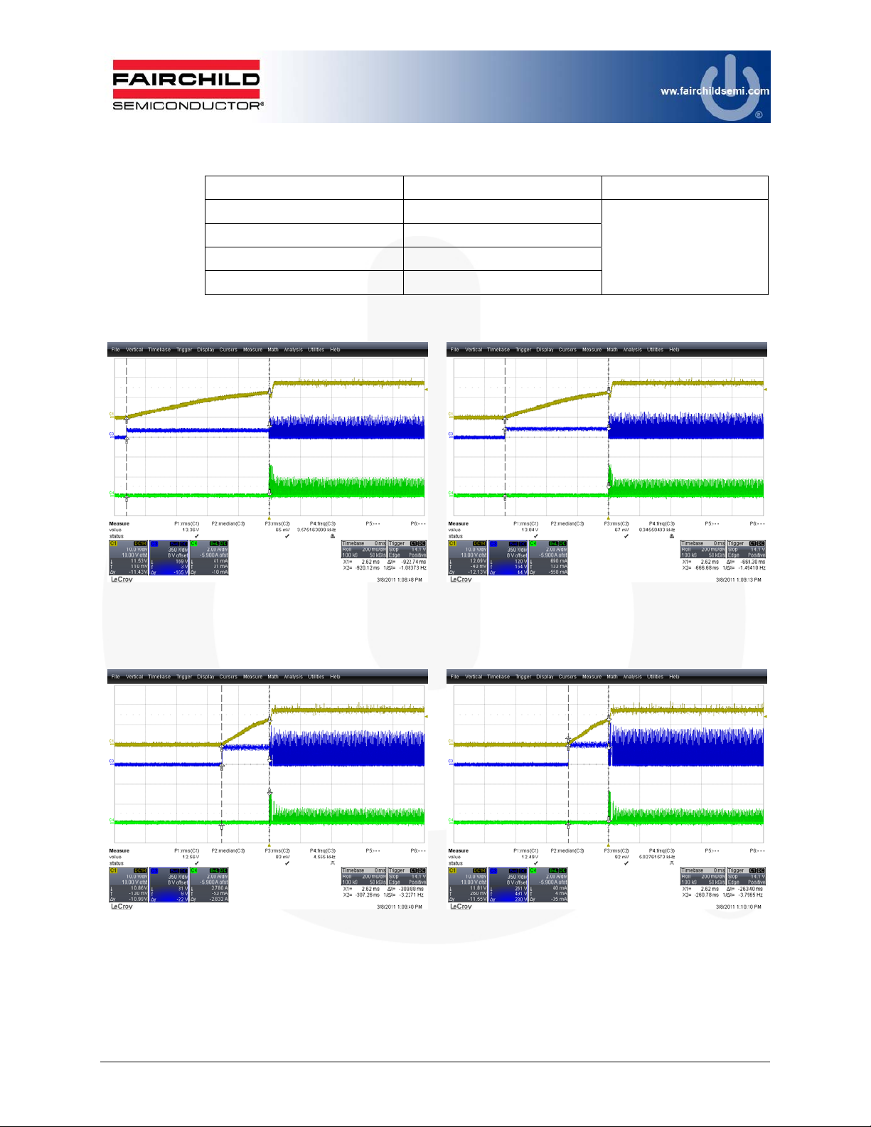
Figure 21 through Figure 24 show the typical startup performance of the Flyback circuit
V
VAC/
VAC/
VAC/
on the board.
Input Voltage Turn-On Time Remark
90VAC / 60Hz 0.922s
115VAC / 60Hz 0.669s
230VAC / 60Hz 0.309s
265VAC / 60Hz 0.263s
< 1s
Figure 21. 90
/ 60Hz, CH1 (Yellow): VCC, CH3
AC
(Blue): V
, CH4 (Green): IDS
DS
Figure 23. 230
CH3 (Blue): V
60Hz CH1 (Yellow): VCC,
, CH4 (Green): IDS
DS
Figure 22. 115
CH3 (Blue): V
Figure 24. 265
CH3 (Blue): V
60Hz, CH1 (Yellow): VCC,
, CH4 (Green): IDS
DS
60Hz ,CH1 (Yellow): VCC,
, CH4 (Green): IDS
DS
© 2012 Fairchild Semiconductor Corporation 21 FEB-L010_FL6961 • Rev. 1.0.0
Page 22
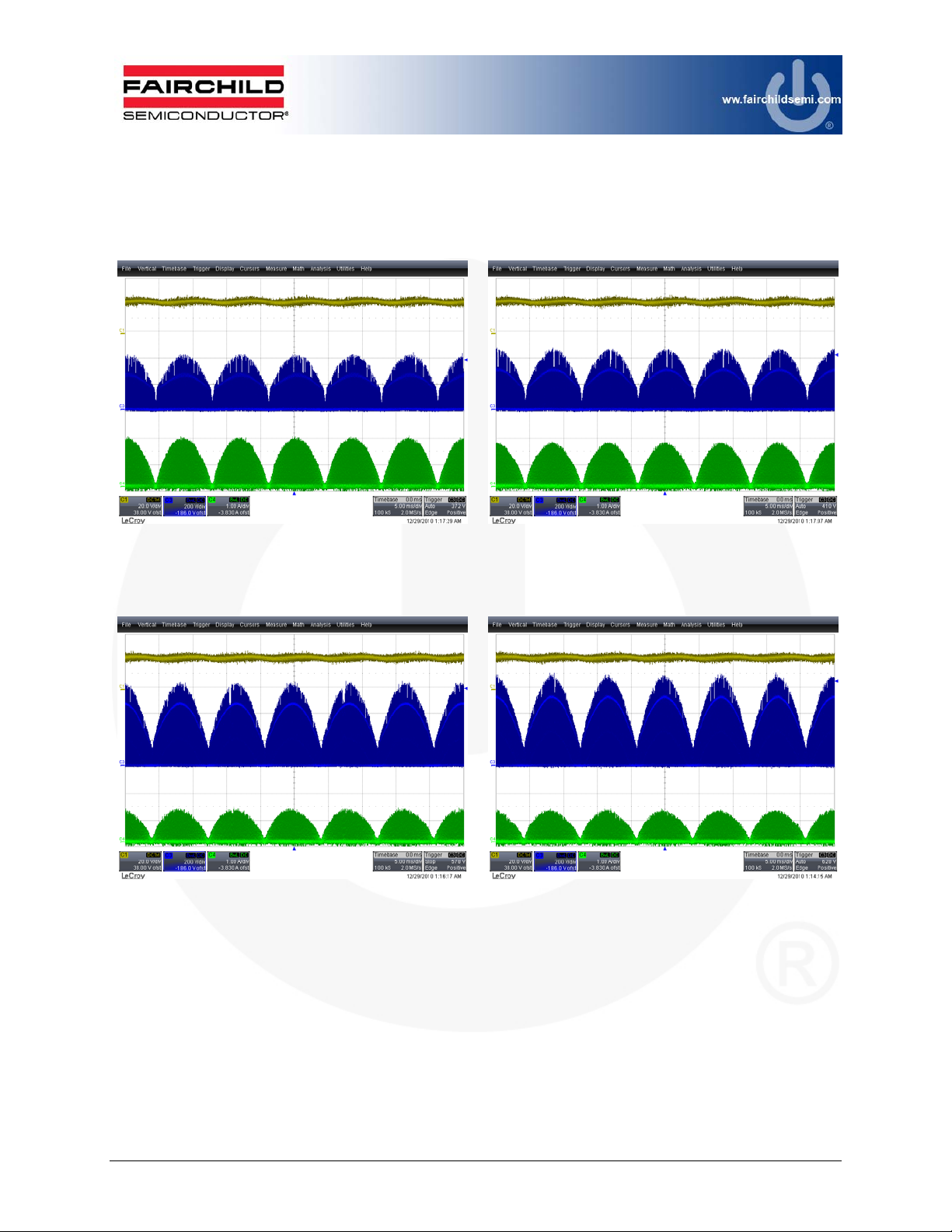
3.8 Operation Waveforms
V
VAC/
V
VAC/
Figure 25 through Figure 28 show the normal operation waveforms on the board at
different input voltage conditions. The output voltage maintains the output level with
120Hz ripple voltage.
Figure 25. 90
/ 60Hz, CH1 (Yellow): VO, CH3
AC
(Blue): V
, CH4 (Green): IDS
DS
Figure 26. 115
CH3 (Blue): V
60Hz, CH1 (Yellow): VO,
, CH4 (Green): IDS
DS
Figure 27. 230
CH3 (Blue): V
/ 60Hz, CH1 (Yellow): VO,
AC
, CH4 (Green): IDS
DS
Figure 28. 265
CH3 (Blue): V
60Hz, CH1 (Yellow): VO,
, CH4 (Green): IDS
DS
© 2012 Fairchild Semiconductor Corporation 22 FEB-L010_FL6961 • Rev. 1.0.0
Page 23
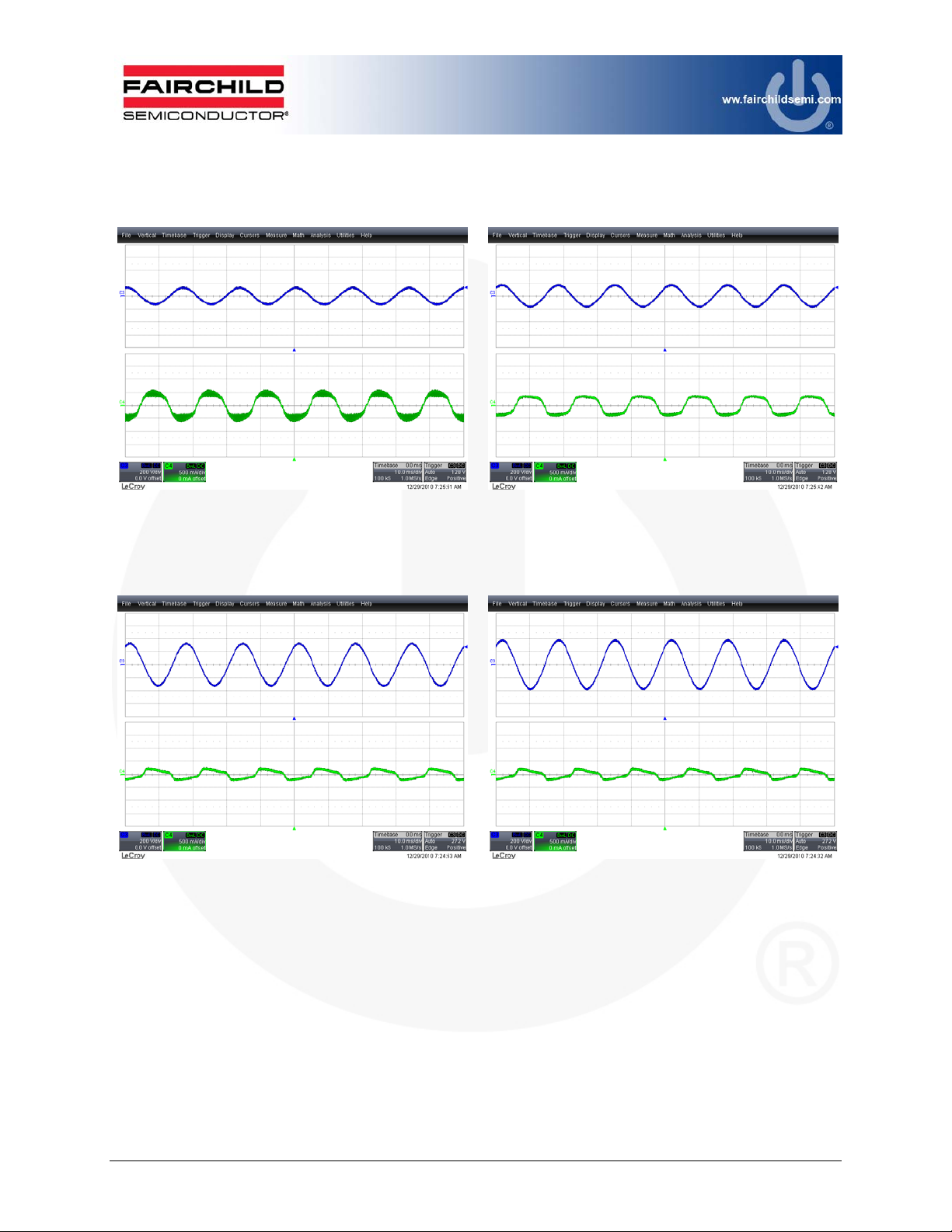
Figure 29 through Figure 32 show the input current waveforms on the board at different
V
VAC/
V
VAC/
input voltage conditions.
Figure 29. 90
/ 60Hz, CH3 (Blue): VIN,
AC
CH4 (Green): I
IN
Figure 30. 115
Figure 31. 230
/ 60Hz, CH3 (Blue): VIN,
AC
CH4 (Green): I
IN
Figure 32. 265
60Hz, CH3 (Blue): VIN,
CH4 (Green): I
IN
60Hz, CH3 (Blue): VIN,
CH4 (Green): I
IN
© 2012 Fairchild Semiconductor Corporation 23 FEB-L010_FL6961 • Rev. 1.0.0
Page 24
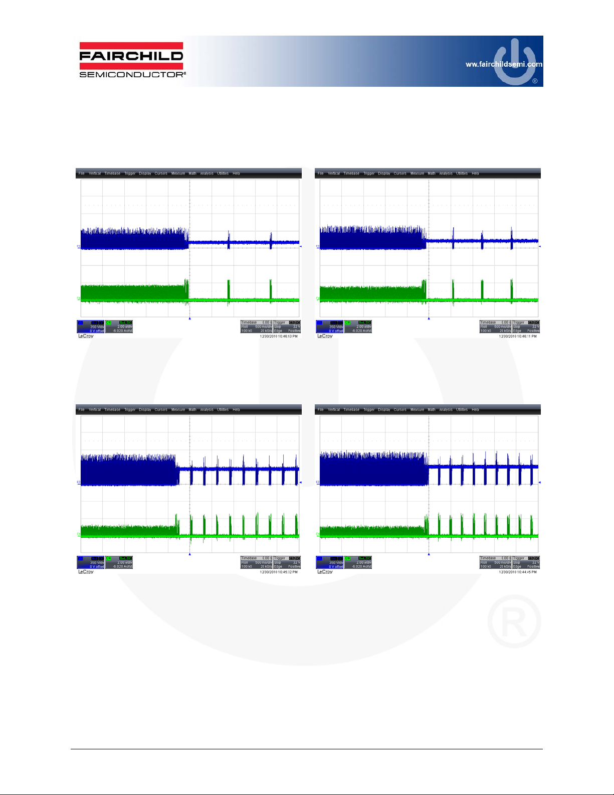
3.9 Short-Circuit Protection
V
VAC/
V
VAC/
Figure 33 through Figure 36 show the typical output waveforms at short load condition.
The IC repeats ON and OFF functions in this mode.
Figure 33. 90
Figure 35. 230
/ 60Hz, CH3 (Blue): VDS,
AC
CH4 (Green): I
/ 60Hz, CH3 (Blue): VDS,
AC
CH4 (Green): I
DS
DS
Figure 34. 115
Figure 36. 265
60Hz, CH3 (Blue): VDS,
CH4 (Green): I
60Hz, CH3 (Blue): VDS,
CH4 (Green): I
DS
DS
© 2012 Fairchild Semiconductor Corporation 24 FEB-L010_FL6961 • Rev. 1.0.0
Page 25
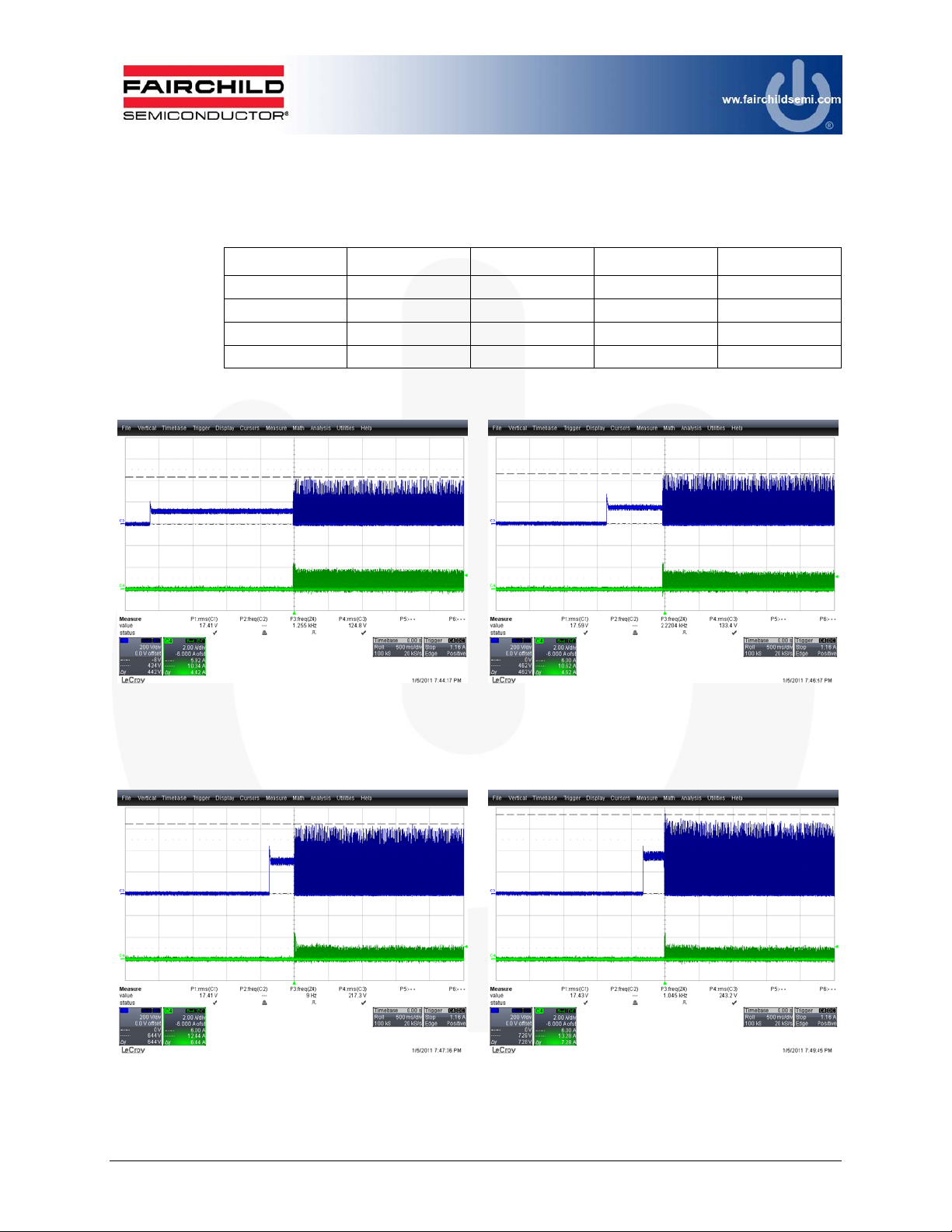
3.10 Stress of the MOSFET & Rectifier
V
VAC/
V
VAC/
Figure 37 through Figure 40 show the voltage stress on the MOSFET at startup with the
rated load condition.
90VAC / 60Hz 115VAC / 60Hz 230VAC / 60Hz 265VAC / 60Hz
MOSFET (VDS) 442V 462V 644V 728V
MOSFET (IDS) 2.36A 2.38A 2.46A 2.42A
Rectifier (VAK) 54.5V 60.5V 84.5V 90.5V
Rectifier (IAK) 3.50A 3.32A 3.54A 3.42A
Figure 37. 90
Figure 39. 230
/ 60Hz, CH3 (Blue): VDS,
AC
CH4 (Green): I
/ 60Hz, CH3 (Blue): VDS,
AC
CH4 (Green): I
DS
DS
Figure 38. 115
Figure 40. 265
60Hz, CH3 (Blue): VDS,
CH4 (Green): I
60Hz, CH3 (Blue): VDS,
CH4 (Green): I
DS
DS
© 2012 Fairchild Semiconductor Corporation 25 FEB-L010_FL6961 • Rev. 1.0.0
Page 26
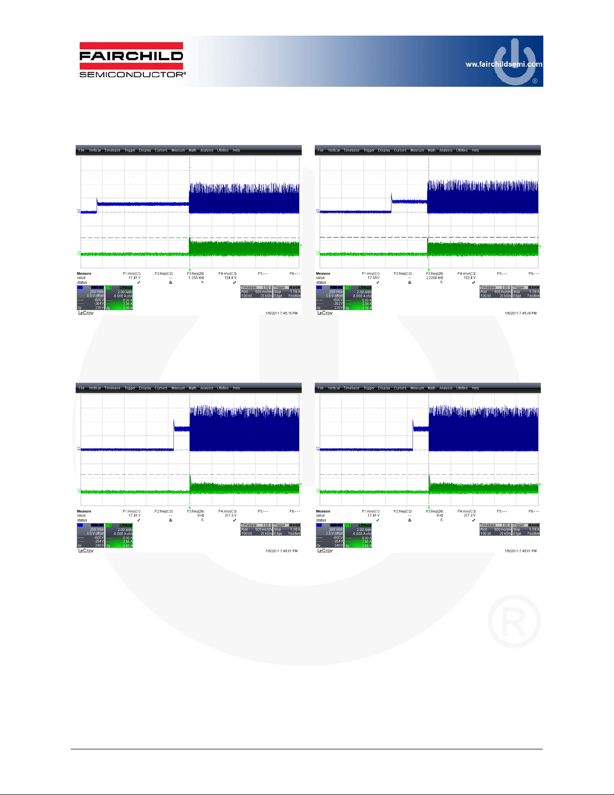
Figure 41 through Figure 44 show the current stress on the MOSFET at startup with the
V
VAC/
V
VAC/
rated load condition.
Figure 41. 90
Figure 43. 230
/ 60Hz, CH3 (Blue): VDS,
AC
CH4 (Green): I
/ 60Hz, CH3 (Blue): VDS,
AC
CH4 (Green): I
DS
DS
Figure 42. 115
Figure 44. 265
60Hz, CH3 (Blue): VDS,
CH4 (Green): I
60Hz, CH3 (Blue): VDS,
CH4 (Green): I
DS
DS
© 2012 Fairchild Semiconductor Corporation 26 FEB-L010_FL6961 • Rev. 1.0.0
Page 27
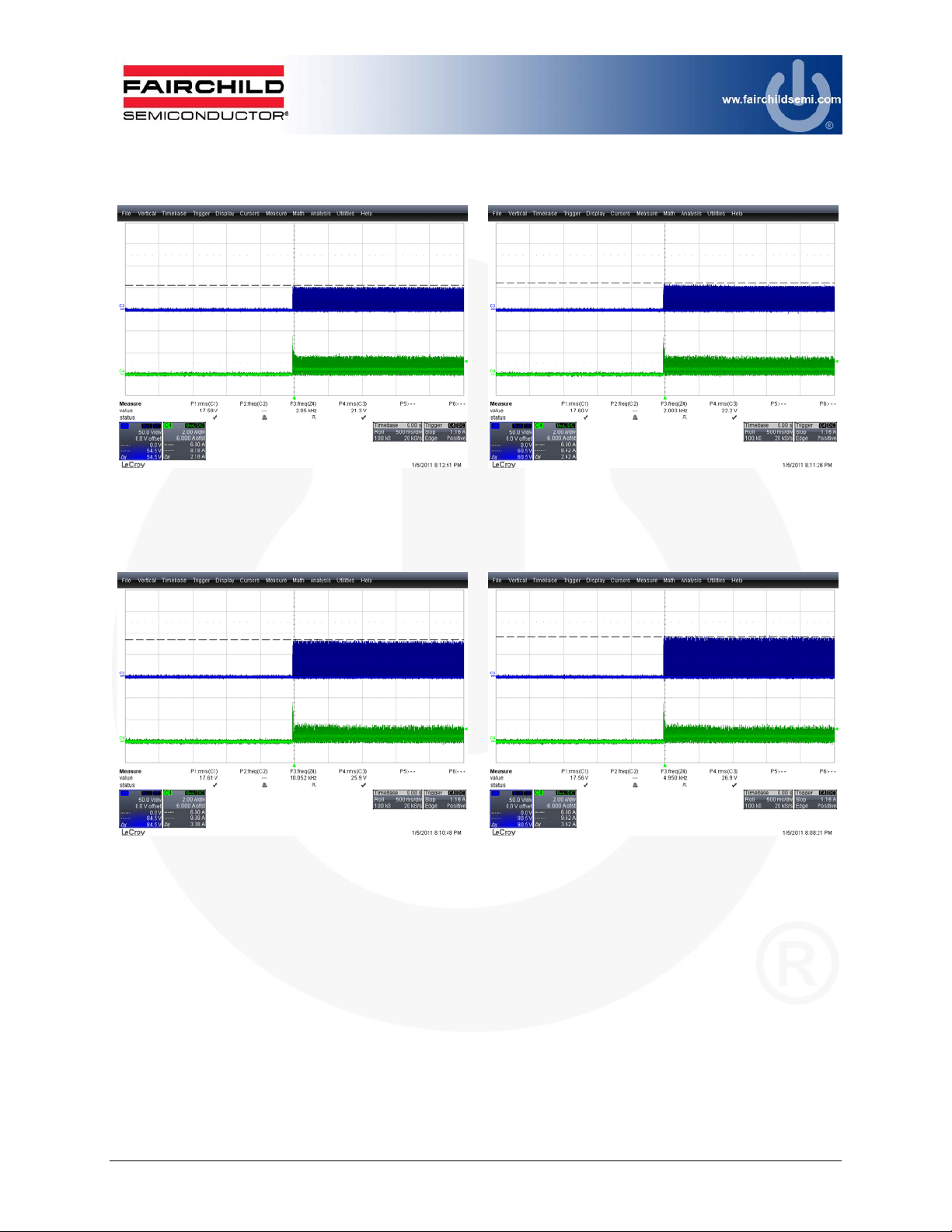
Figure 45 through Figure 48 show the voltage stress on the output rectifier at startup with
V
VAC/
V
VAC/
the rated load condition.
Figure 45. 90
/ 60Hz, CH3 (Blue): VAK,
AC
CH4 (Green): I
AK
Figure 46. 115
60Hz, CH3 (Blue): VAK,
CH4 (Green): I
AK
Figure 47. 230
/ 60Hz, CH3 (Blue): VAK,
AC
CH4 (Green): I
AK
Figure 48. 265
60Hz, CH3 (Blue): VAK,
CH4 (Green): I
AK
© 2012 Fairchild Semiconductor Corporation 27 FEB-L010_FL6961 • Rev. 1.0.0
Page 28
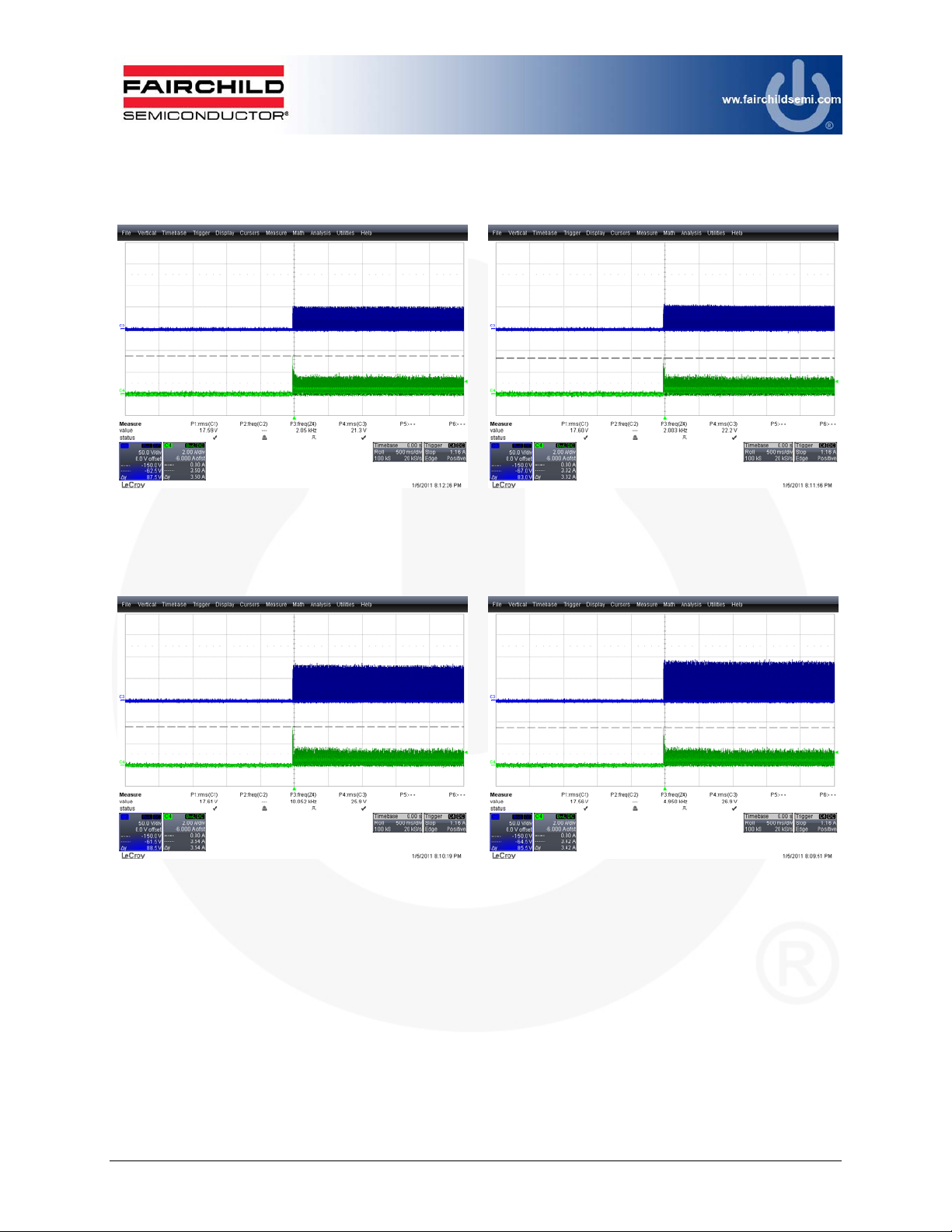
Figure 49 throgh Figure 52 show the current stress on the output rectifier at startup with
V
VAC/
V
VAC/
the rated load condition.
Figure 49. 90
Figure 51. 230
/ 60Hz, CH3 (Blue): VAK,
AC
CH4 (Green): I
/ 60Hz, CH3 (Blue): VAK,
AC
CH4 (Green): I
AK
AK
Figure 50. 115
Figure 52. 265
60Hz, CH3 (Blue): VAK,
CH4 (Green): I
60Hz, CH3 (Blue): VAK,
CH4 (Green): I
AK
AK
© 2012 Fairchild Semiconductor Corporation 28 FEB-L010_FL6961 • Rev. 1.0.0
Page 29
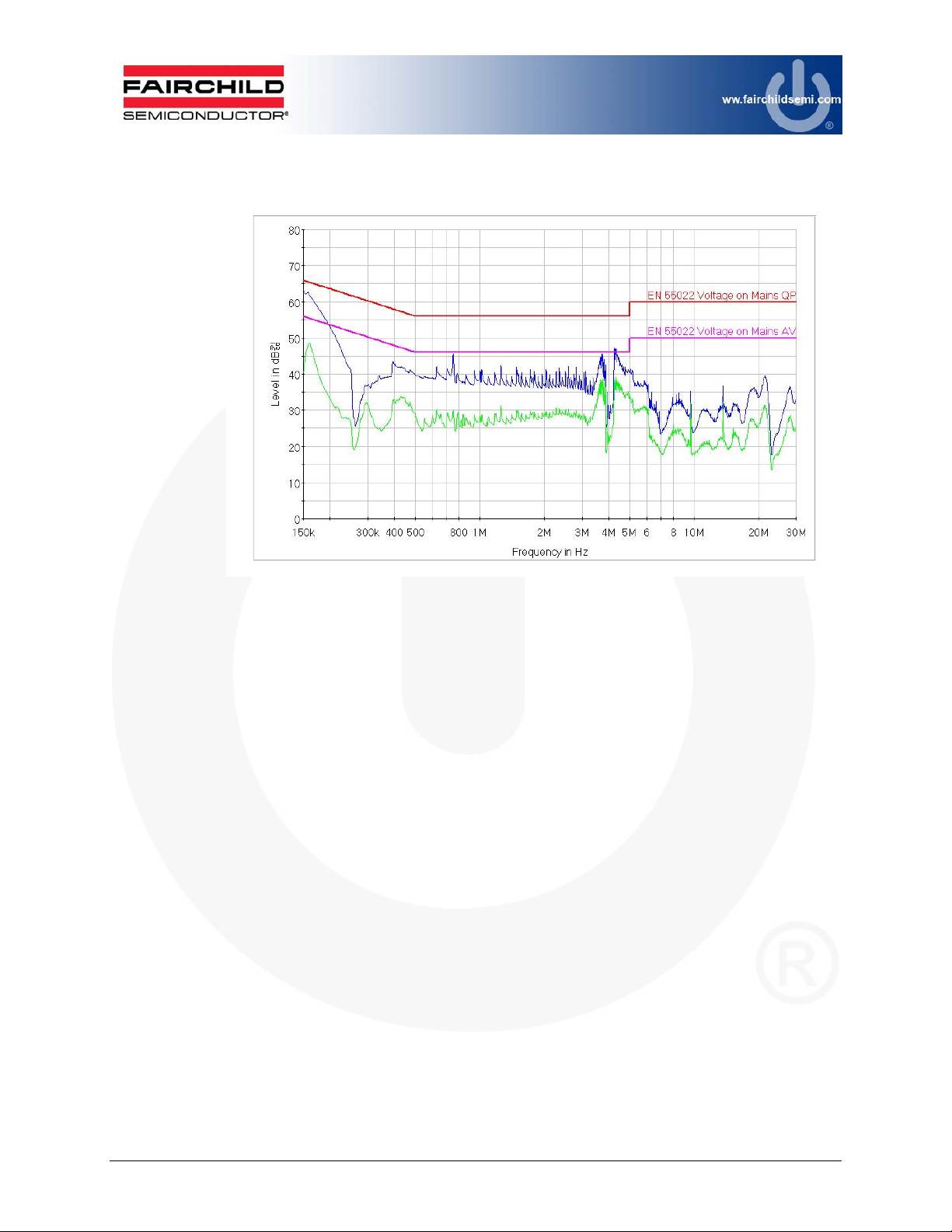
3.11 Stress of the MOSFET & Rectifier
All measurements were conducted in observance of CISPR22 criteria.
Figure 53. EMI Results, Conducted Emission-Line at 230VAC, Full Load
(24V/1.25A; 6 Series, 2 Parallel LEDs)
© 2012 Fairchild Semiconductor Corporation 29 FEB-L010_FL6961 • Rev. 1.0.0
Page 30

4. Revision History
Rev. Date Description
1.0.0 5/22/12 Initial Release
WARNING AND DISCLAIMER
Replace components on the Evaluation Board only with those parts shown on the parts list (or Bill of Materials) in the Users’ Guide. Contact an
authorized Fairchild representative with any questions.
This board is intended to be used by certified professionals, in a lab environment, following proper safety procedures. Use at your own risk. The
Evaluation board (or kit) is for demonstration purposes only and neither the Board nor this User’s Guide constitute a sales contract or create any kind
of warranty, whether express or implied, as to the applications or products involved. Fairchild warrantees that its products meet Fairchild’s published
specifications, but does not guarantee that its products work in any specific application. Fairchild reserves the right to make changes without notice to
any products described herein to improve reliability, function, or design. Either the applicable sales contract signed by Fairchild and Buyer or, if no
contract exists, Fairchild’s standard Terms and Conditions on the back of Fairchild invoices, govern the terms of sale of the products described herein.
DISCLAIMER
FAIRCHILD SEMICONDUCTOR RESERVES THE RIGHT TO MAKE CHANGES WITHOUT FURTHER NOTICE TO ANY PRODUCTS HEREIN TO
IMPROVE RELIABILITY, FUNCTION, OR DESIGN. FAIRCHILD DOES NOT ASSUME ANY LIABILITY ARISING OUT OF THE APPLICATION OR
USE OF ANY PRODUCT OR CIRCUIT DESCRIBED HEREIN; NEITHER DOES IT CONVEY ANY LICENSE UNDER ITS PATENT RIGHTS, NOR
THE RIGHTS OF OTHERS.
LIFE SUPPORT POLICY
FAIRCHILD’S PRODUCTS ARE NOT AUTHORIZED FOR USE AS CRITICAL COMPONENTS IN LIFE SUPPORT DEVICES OR SYSTEMS
WITHOUT THE EXPRESS WRITTEN APPROVAL OF THE PRESIDENT OF FAIRCHILD SEMICONDUCTOR CORPORATION.
As used herein:
1. Life support devices or systems are devices or systems which, (a)
are intended for surgical implant into the body, or (b) support or
sustain life, or (c) whose failure to perform when properly used in
accordance with instructions for use provided in the labeling, can be
reasonably expected to result in significant injury to the user.
ANTI-COUNTERFEITING POLICY
Fairchild Semiconductor Corporation's Anti-Counterfeiting Policy. Fairchild's Anti-Counterfeiting Policy is also stated on our external website,
www.fairchildsemi.com, under Sales Support.
Counterfeiting of semiconductor parts is a growing problem in the industry. All manufacturers of semiconductor products are experiencing
counterfeiting of their parts. Customers who inadvertently purchase counterfeit parts experience many problems such as loss of brand reputation,
substandard performance, failed applications, and increased cost of production and manufacturing delays. Fairchild is taking strong measures to
protect ourselves and our customers from the proliferation of counterfeit parts. Fairchild strongly encourages customers to purchase Fairchild parts
either directly from Fairchild or from Authorized Fairchild Distributors who are listed by country on our web page cited above. Products customers buy
either from Fairchild directly or from Authorized Fairchild Distributors are genuine parts, have full traceability, meet Fairchild's quality standards for
handling and storage and provide access to Fairchild's full range of up-to-date technical and product information. Fairchild and our Authorized
Distributors will stand behind all warranties and will appropriately address any warranty issues that may arise. Fairchild will not provide any warranty
coverage or other assistance for parts bought from Unauthorized Sources. Fairchild is committed to combat this global problem and encourage our
customers to do their part in stopping this practice by buying direct or from authorized distributors.
EXPORT COMPLIANCE STATEMENT
These commodities, technology, or software were exported from the United States in accordance with the Export Administration Regulations for the
ultimate destination listed on the commercial invoice. Diversion contrary to U.S. law is prohibited.
U.S. origin products and products made with U.S. origin technology are subject to U.S Re-export laws. In the event of re-export, the user will be
responsible to ensure the appropriate U.S. export regulations are followed.
2. A critical component is any component of a life support device or
system whose failure to perform can be reasonably expected to
cause the failure of the life support device or system, or to affect its
safety or effectiveness.
© 2012 Fairchild Semiconductor Corporation 30 FEB-L010_FL6961 • Rev. 1.0.0
 Loading...