

Page 1
March 1998
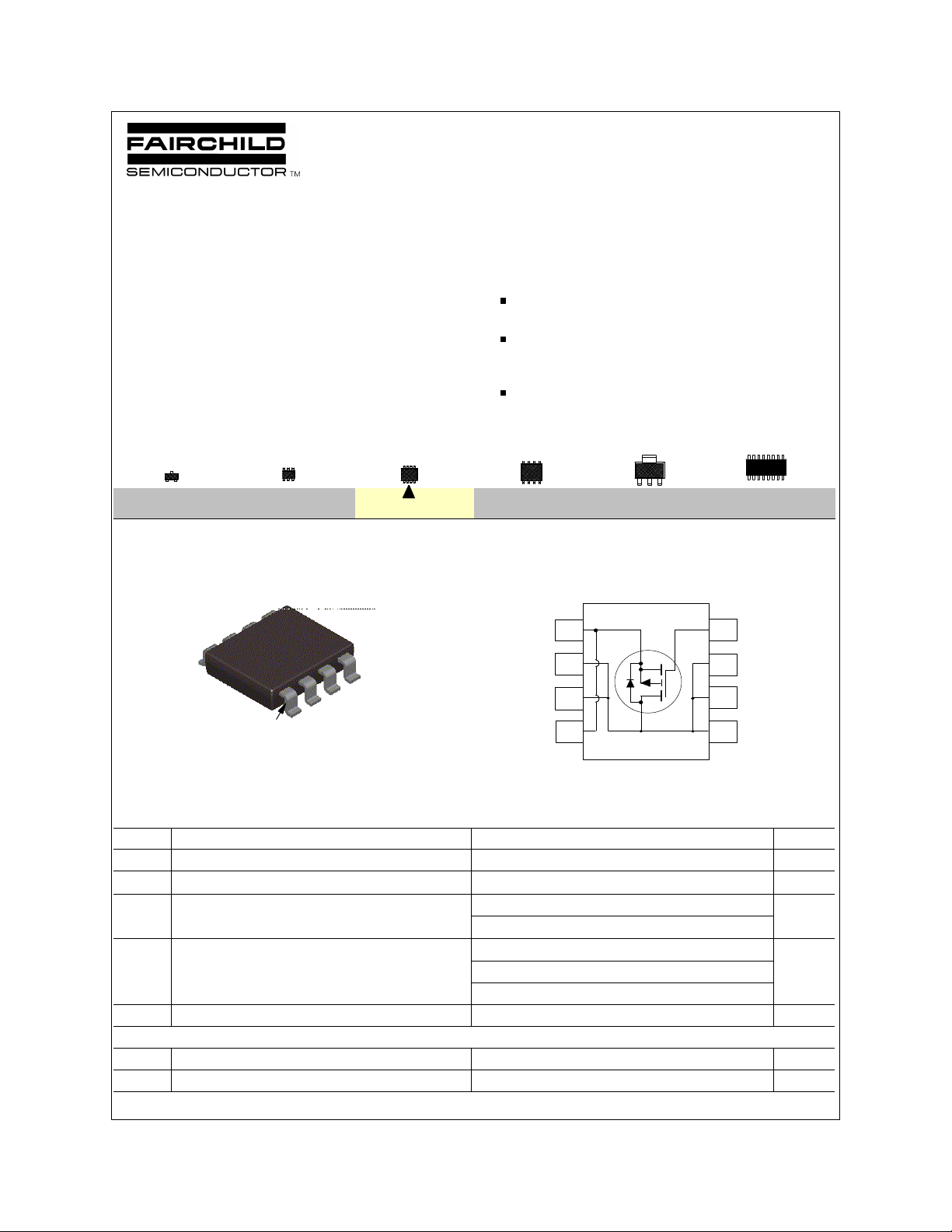
FDR856P
P-Channel Logic Level Enhancement Mode Field Effect Transistor
General Description Features
SuperSOTTM-8 P-Channel enhancement mode power field
effect transistors are produced using Fairchild's
proprietary, high cell density, DMOS technology. This very
high density process is especially tailored to minimize
on-state resistance and provide superior switching
performance. These devices are particularly suited for low
voltage applications such as battery powered circuits or
portable electronics where low in-line power loss, fast
switching and resistance to transients are needed.
- 6.3 A, -30 V, R
R
SuperSOTTM-8 package:
small footprint (40% less than SO-8);low profile (1mm
thick);maximum power comperable to SO-8.
High density cell design for extremely low R
=0.025 Ω @ VGS = -10 V
DS(ON)
=0.040 Ω @ VGS = -4.5 V.
DS(ON)
DS(ON)
.
SOT-23
SuperSOTTM-6
SuperSOTTM-8
SO-8 SOT-223
SOIC-16
S
D
D
5
4
S
856P
pin 1
SuperSOT -8
TM
Absolute Maximum Ratings T
D
G
D
D
= 25oC unless other wise noted
A
6
7
8
Symbol Parameter FDR856P Units
V
DSS
V
GSS
I
D
Drain-Source Voltage -30 V
Gate-Source Voltage - Continuous ±20 V
Maximum Drain Current - Continuous (Note 1a) -5.1 A
- Pulsed -50
P
D
TJ,T
Maximum Power Dissipation (Note 1a) 1.8 W
(Note 1b)
(Note 1c)
Operating and Storage Temperature Range -55 to 150 °C
STG
1
0.9
THERMAL CHARACTERISTICS
R
JA
θ
R
JC
θ
Thermal Resistance, Junction-to-Ambient (Note 1a) 50 °C/W
Thermal Resistance, Junction-to-Case (Note 1) 25 °C/W
3
2
1
© 1998 Fairchild Semiconductor Corporation
FDR856P Rev.B
Page 2
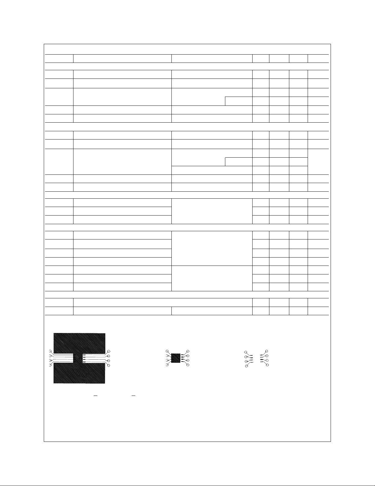
Electrical Characteristics (T
= 25 OC unless otherwise noted )
A
Symbol Parameter Conditions Min Typ Max Units
OFF CHARACTERISTICS
BV
∆BV
I
DSS
I
GSSF
I
GSSR
DSS
DSS
Drain-Source Breakdown Voltage VGS = 0 V, I D = -250 µA -30 V
Breakdown Voltage Temp. Coefficient
/∆T
J
Zero Gate Voltage Drain Current
ID = -250 µA, Referenced to 25 oC
VDS = -24 V, V
GS
= 0 V
-15
-1 µA
TJ = 55°C
Gate - Body Leakage, Forward VGS = -20 V, VDS = 0 V -100 nA
Gate - Body Leakage, Reverse
VGS = -20 V, V
DS
= 0 V
mV /oC
-10 µA
-100 nA
ON CHARACTERISTICS (Note 2)
V
∆V
R
GS(th)
GS(th)
DS(ON)
Gate Threshold Voltage VDS = VGS, ID = -250 µA -1 -1.5 -3 V
Gate Threshold Voltage Temp. Coefficient
/∆T
J
Static Drain-Source On-Resistance
ID = -250 µA, Referenced to 25 oC
VGS = -10 V, I D = -6.3 A
3
0.022 0.025
mV /oC
TJ =125°C 0.03 0.042
0.033 0.04
15 S
I
g
D(ON)
FS
VGS = -4.5 V, I D = -5 A
On-State Drain Current VGS = -10 V, VDS = -5 V -50 A
Forward Transconductance
VDS = -10 V, I D = -6.3 A
DYNAMIC CHARACTERISTICS
C
iss
C
oss
C
rss
Input Capacitance VDS = -15 V, VGS = 0 V,
Output Capacitance 740 pF
f = 1.0 MHz
1370 pF
Reverse Transfer Capacitance 220 pF
SWITCHING CHARACTERISTICS (Note 2)
t
t
t
t
Q
Q
Q
D(on)
r
D(off)
f
Turn - On Delay Time
Turn - On Rise Time
V
= -15 V, I D= -1 A
DS
VGS = -10 V , RG = 6 Ω
Turn - Off Delay Time 80 100 ns
Turn - Off Fall Time 130 160 ns
g
gs
gd
Total Gate Charge
Gate-Source Charge
Gate-Drain Charge 8.7 nC
VDS = -15 V, I D = -6.3 A,
V
= -10 V
GS
7 14 ns
12 19 ns
22 31 nC
3.8 nC
DRAIN-SOURCE DIODE CHARACTERISTICS AND MAXIMUM RATINGS
I
S
V
Notes:
1. R
SD
JA
θ
design while R
Maximum Continuous Drain-Source Diode Forward Current -1.3 A
Drain-Source Diode Forward Voltage
is the sum of the junction-to-case and case-to-ambient thermal resistance where the case thermal reference is defined as the solder mounting surface of the drain pins. R
is determined by the user's board design.
CA
θ
VGS = 0 V, IS = -1.3 A
(Note 2)
-0.73 -1.2 V
is guaranteed by
JC
θ
Ω
a. 50OC/W on a 0.5 in
pad of 2oz copper.
Scale 1 : 1 on letter size paper
2. Pulse Test: Pulse Width < 300µs, Duty Cycle < 2.0%.
2
b. 105OC/W on a 0.02 in
pad of 2oz copper.
2
c. 125OC/W on a 0.003 in2 pad
of 2oz copper.
FDR856P Rev.B
Page 3
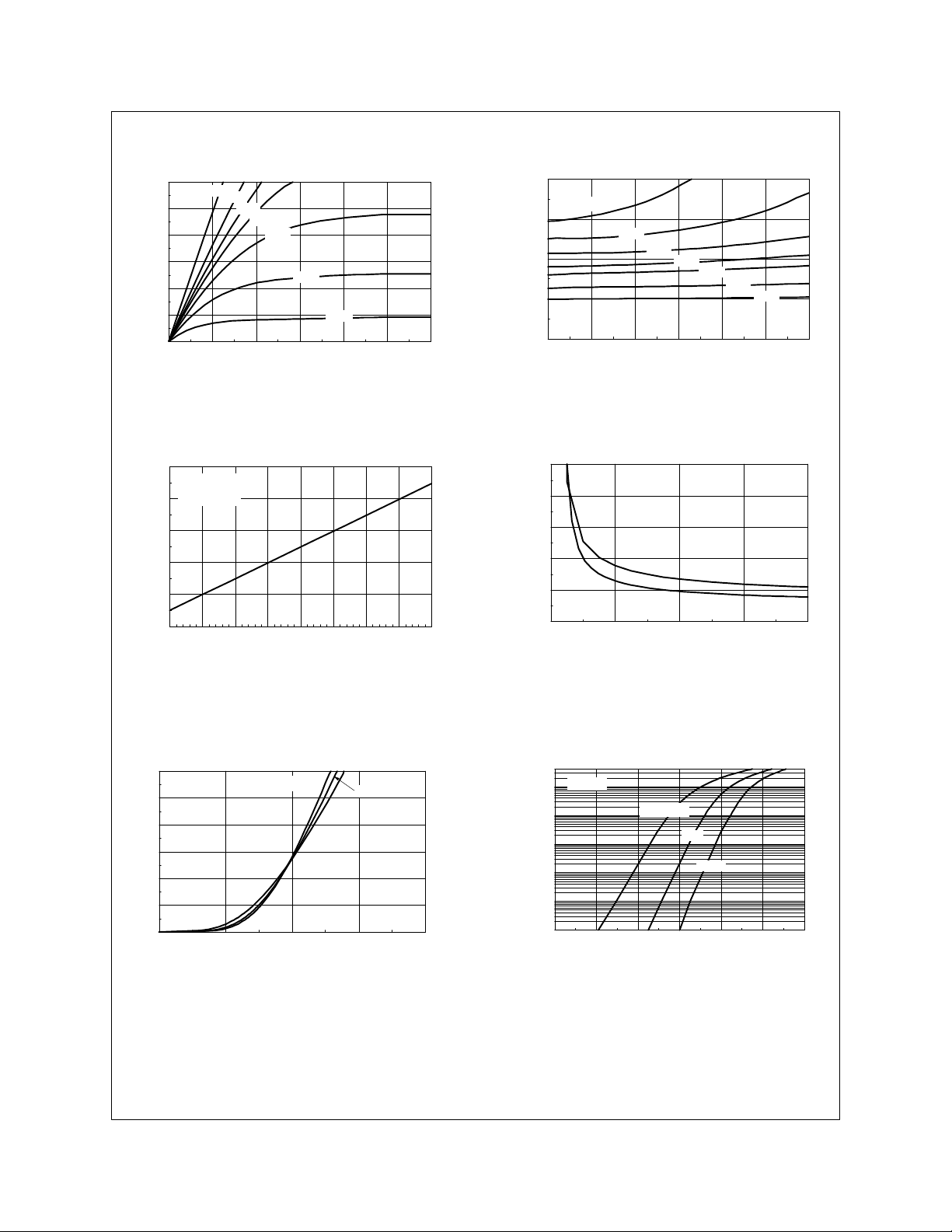
Typical Electrical Characteristics
30
V = -10V
GS
-5.5V
25
20
15
10
5
D
- I , DRAIN-SOURCE CURRENT (A)
0
0 0.5 1 1.5 2 2.5 3
-4.5V
-4.0V
-3.5V
-3.0V
-2.5V
-V , DRAIN-SOURCE VOLTAGE (V)
DS
Figure 1. On-Region Characteristics.
1.6
I = -6.3A
D
V = -10V
1.4
GS
1.2
1
DS(ON)
R , NORMALIZED
0.8
DRAIN-SOURCE ON-RESISTANCE
0.6
-50 -25 0 25 50 75 100 125 150
T , JUNCTION TEMPERATURE (°C)
J
2.5
V = -3.5 V
GS
2
1.5
DS(on)
R , NORMALIZED
1
DRAIN-SOURCE ON-RESISTANCE
0.5
0 5 10 15 20 25 30
Figure 2. On-Resistance Variation with
Drain Current and Gate Voltage.
0.125
0.1
0.075
0.05
0.025
DS(ON)
R , ON-RESISTANCE (OHM)
0
2 4 6 8 10
-4.0V
-4.5V
-5.0V
-5.5V
-7.0V
- I , DRAIN CURRENT (A)
D
T = 125°C
J
T = 25°C
J
-V , GATE TO SOURCE VOLTAGE (V)
GS
-10V
I = -3A
D
Figure 3. On-Resistance Variation with
Temperature.
30
V = -5V
DS
25
20
15
10
D
- I , DRAIN CURRENT (A)
5
0
1 2 3 4 5
-V , GATE TO SOURCE VOLTAGE (V)
GS
T = -55°C
J
25°C
125°C
Figure 4 . On Resistance Variation with
Gate-to-Source Voltage.
40
V = 0V
GS
5
1
0.1
0.01
0.001
S
-I , REVERSE DRAIN CURRENT (A)
0.0001
0 0.2 0.4 0.6 0.8 1 1.2
-V , BODY DIODE FORWARD VOLTAGE (V)
T = 125°C
J
25°C
-55°C
SD
Figure 5 . Transfer Characteristics. Figure 6 . Body Diode Forward Voltage
Variation with Source
Current and Temperature.
FDR856P Rev.B
Page 4
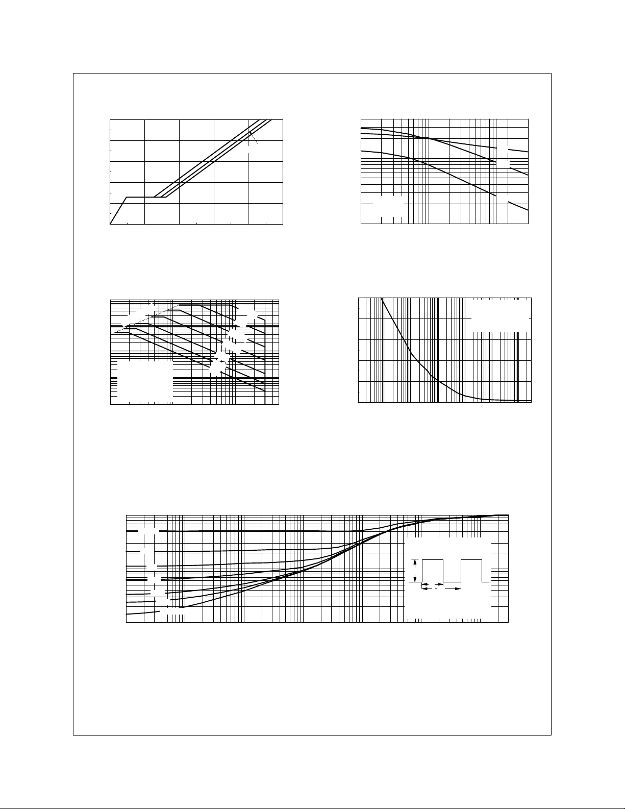
Typical Electrical Characteristics (continued)
10
8
I = -6.3A
D
V = -5V
DS
-15V
6
4
2
GS
-V , GATE-SOURCE VOLTAGE (V)
0
0 8 16 24 32 40
Q , GATE CHARGE (nC)
g
Figure 7. Gate Charge Characteristics.
80
RDS(ON) LIMIT
5
0.5
V = -10V
GS
SINGLE PULSE
D
-I , DRAIN CURRENT (A)
R = 135°C/W
0.05
0.01
JA
θ
T = 25°C
A
A
0.1 0.2 0.5 1 2 5 10 20 50
-V , DRAIN-SOURCE VOLTAGE (V)
DS
DC
100us
1ms
10ms
100ms
1s
10s
-10V
4000
2000
1000
500
CAPACITANCE (pF)
f = 1 MHz
200
V = 0 V
GS
100
0.1 0.3 1 3 7 15 30
-V , DRAIN TO SOURCE VOLTAGE (V)
DS
C
iss
C
oss
C
rss
Figure 8. Capacitance Characteristics.
50
40
30
20
POWER (W)
10
0
0.0001 0.001 0.01 0.1 1 10 100 300
SINGLE PULSE TIME (SEC)
SINGLE PULSE
R = 135°C/W
JA
θ
T = 25°C
A
Figure 9. Maximum Safe Operating Area.
Figure 10. Single Pulse Maximum Power
Dissipation.
1
D = 0.5
0.5
0.3
0.2
0.2
0.1
0.05
0.03
r(t), NORMALIZED EFFECTIVE
0.02
TRANSIENT THERMAL RESISTANCE
0.01
0.1
0.05
0.02
0.01
Single Pulse
0.0001 0.001 0.01 0.1 1 10 100 300
Figure 11. Transient Thermal Response Curve.
Thermal characterization performed using the conditions described in Note 1c.
Transient thermal response will change depending on the circuit board design.
t , TIME (sec)
1
R (t) = r(t) * R
JA
θ
R = 135
JA
θ
P(pk)
t
1
t
2
T - T = P * R (t)
J
A
Duty Cycle, D = t / t
°C/W
JA
θ
1
θ
JA
2
FDR856P Rev.B
Page 5
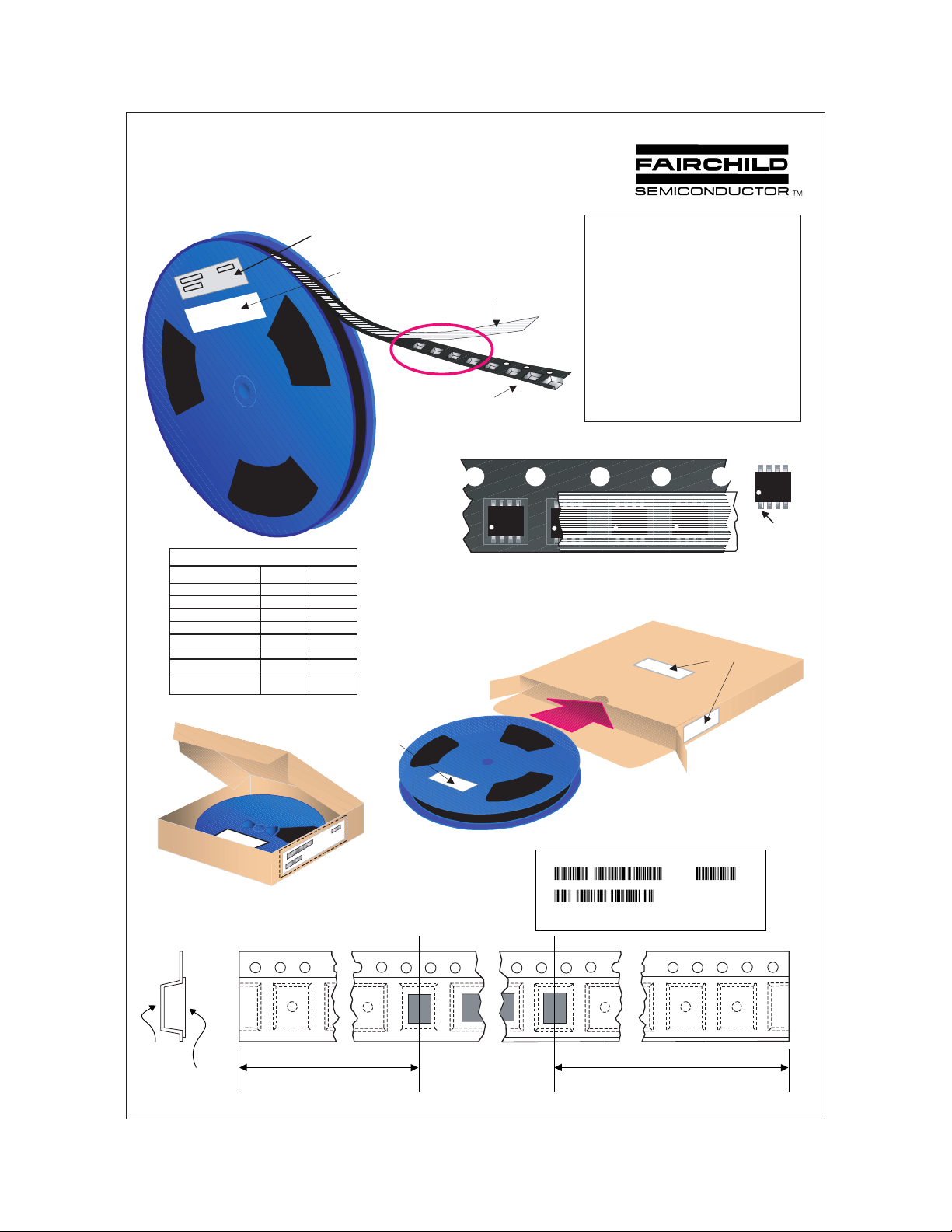
SuperSOTTM-8 Tape and Reel Data and Package Dimensions
SSOT-8 Packaging
Configuration: Figure 1.0
Customized Label
F63TNR Label
Emboss ed Carrier Tape
Antistatic Cover Tape
Static Dissipative
852
F
831N
Packaging Description:
SSOT-8 parts are shipped in tape. The carrier tape is
made from a di ssi pati ve (c arbo n fi lled) po lycarbon ate
resin. The cov er tap e is a mu lt ilayer film (Heat Act ivat ed
Adhesiv e in nat ure) prim aril y c omp osed of po lyes ter film ,
adhesive layer, sealant, and anti-static sprayed agent.
These reeled parts in standar d option are ship ped wi th
3,000 u n i ts per 13" or 330c m d i a m et er re el . The r e el s are
dark blue in color and is made of po ly s t yr ene plas ti c (antistatic c oated). Other option comes in 500 units per 7" or
177c m diam eter reel. This and s ome o ther opt ion s are
furth er described in th e Packaging Information table.
These full reels are in dividu ally barc ode labeled and
placed in side a standard intermediat e box (illus trated in
figur e 1.0) made of recyclable corr ugated brown pa per.
One box cont ains t wo reels maxi mum. And t hese bo xes
are placed ins ide a barc ode labeled shipp ing bo x whic h
co m e s i n di ff e r e n t sizes de pe ndin g on t he nu mbe r of part s
sh i pped.
852
852
F
831N
F
831N
852
F
831N
852
F
831N
Pin 1
SSOT-8 Packaging Information
Packaging Option
Packaging type
Qty per Reel/Tube/Bag
Reel Size
Box Dimension (mm)
Max qty per Box
Weight per unit (gm)
Weight per Reel (kg)
Note/Comments
184mm x 187mm x 47mm
Stan dard
(no flow c ode)
TNR
3,000 500
13" Dia
343x64x343 184x187x47
6,000 1,000
0.0416 0.0416
0.5615 0.0980
D84Z
TNR
7" Dia
F63TNR
Label
Pizza Box for D84Z Option
SSOT-8 Tape Leader and Trailer
Configuration: Figure 2.0
F63TNR
Label
SSOT-8 Unit Orientation
343mm x 342mm x 64mm
Inter mediate bo x for Standard
and L 99Z Options
F63TNR Label sampl e
LOT: CBVK7 41B019
FSID: FDR835N
D/C1: D9842 QTY1: SPEC REV:
D/C2: QTY2: CPN:
F63TNR Label
QTY: 3000
SPEC:
N/F: F (F63TNR)3
Carrier Tape
Cover Tape
Tr ailer Tape
300mm mi nimum or
38 empty pockets
Components
Leader Tape
500mm mi nimum or
62 empty poc k ets
August 1999, Rev. C
Page 6
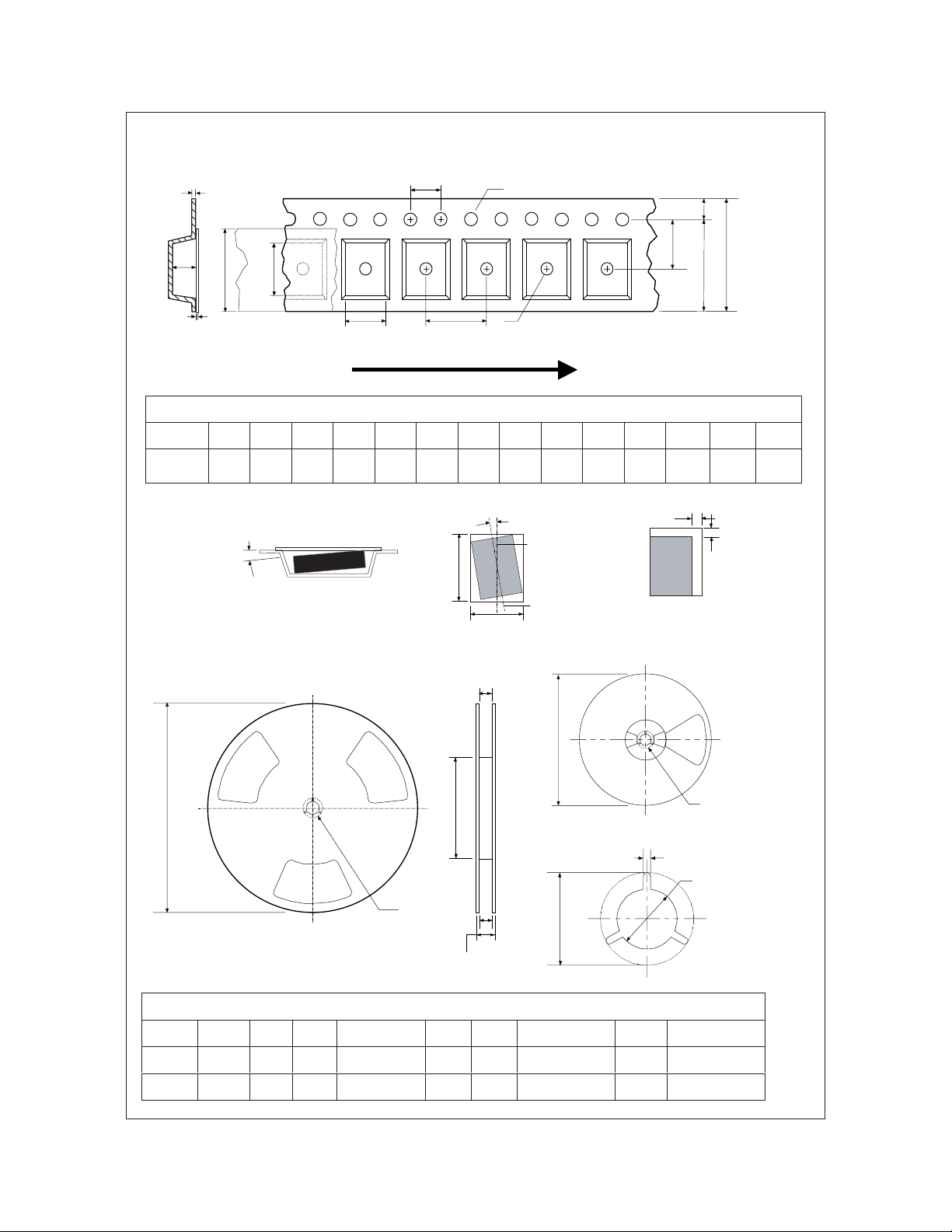
SuperSOTTM-8 Tape and Reel Data and Package Dimensions, continued
SSOT-8 Embossed Carrier Tape
Configuration: Figure 3.0
T
K0
Wc
B0
P0
D0
E1
F
W
E2
Tc
A0
P1
D1
User Direction of Feed
Dimensions are in millimeter
Pkg type
SSOT-8
(12mm)
Notes: A0, B0, and K0 dimensions are determined with respec t to the EIA/Jedec RS-481
rotational and lateral movement requi rements (see sketches A, B, and C).
SSOT-8 Reel Configuration: Figur e 4.0
A0 B0 W D0 D1 E1 E2 F P1 P0 K0 T Wc Tc
4.47
5.00
12.0
1.55
1.50
1.75
10.25
+/-0.10
+/-0.10
20 deg maximum component rotation
Sketc h A (Side or Front Sectional View)
Component Rotation
+/-0.3
+/-0.05
+/-0.10
+/-0.10
B0
Sketc h B (Top View)
Component Rotation
min
5.50
+/-0.05
20 deg maximum
A0
Typical
component
cavity
center line
Typical
component
center line
W1 Measured at Hub
Dim A
Max
8.0
+/-0.1
4.0
+/-0.1
1.37
0.280
+/-0.150
9.5
+/-0.025
0.5mm
maximum
+/-0.10
0.5mm
maximum
Sketc h C (Top View)
Component lateral movement
0.06
+/-0.02
Dim A
max
13" Diameter Option
Tape Size
12mm 7" Dia
12mm 13" Dia
1998 Fairchild Semiconductor Corporation
Reel
Option
Dim A Dim B Dim C Dim D Dim N Dim W1 Dim W2 Dim W3 (LSL-USL)
7.00
177.8
13.00
330
0.059
1.5
0.059
1.5
Dim N
See detail AA
W3
W2 max Measured at Hub
Dimensions are in inches and millimeters
512 +0.020/-0.008
13 +0.5/-0.2
512 +0.020/-0.008
13 +0.5/-0.2
0.795
20.2
0.795
20.2
5.906
150
7.00
178
0.488 +0.078/-0.000
12.4 +2/0
0.488 +0.078/-0.000
12.4 +2/0
Dim D
min
Diameter Option
7"
DETAIL AA
0.724
18.4
0.724
18.4
See detail AA
B Min
Dim C
0.469 – 0.606
11.9 – 15.4
0.469 – 0.606
11.9 – 15.4
July 1999, Rev. C
Page 7
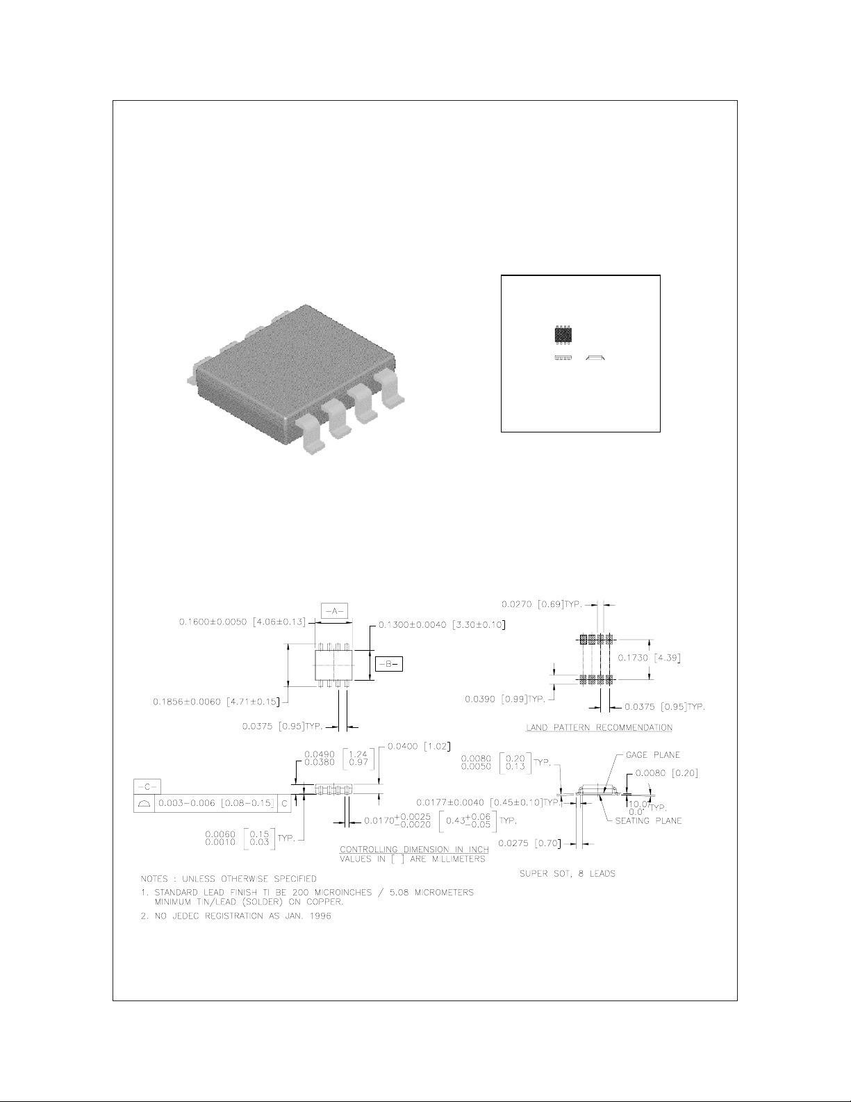
SuperSOTTM-8 Tape and Reel Data and Package Dimensions, continued
SuperSOT-8 (FS PKG Code 34, 35)
1 : 1
Scale 1:1 on letter size paper
Dimensio ns shown below are in:
inches [mil lime ters ]
Part Weight per unit (gram): 0.0416
September 1998, Rev. A
Page 8
TRADEMARKS
The following are registered and unregistered trademarks Fairchild Semiconductor owns or is authorized to use and is
not intended to be an exhaustive list of all such trademarks.
ACEx™
CoolFET™
CROSSVOLT™
2
E
CMOS
TM
FACT™
FACT Quiet Series™
®
FAST
FASTr™
GTO™
HiSeC™
ISOPLANAR™
MICROWIRE™
POP™
PowerTrench
QFET™
QS™
Quiet Series™
SuperSOT™-3
SuperSOT™-6
SuperSOT™-8
SyncFET™
TinyLogic™
UHC™
VCX™
DISCLAIMER
FAIRCHILD SEMICONDUCTOR RESERVES THE RIGHT TO MAKE CHANGES WITHOUT FURTHER
NOTICE TO ANY PRODUCTS HEREIN TO IMPROVE RELIABILITY, FUNCTION OR DESIGN. FAIRCHILD
DOES NOT ASSUME ANY LIABILITY ARISING OUT OF THE APPLICA TION OR USE OF ANY PRODUCT
OR CIRCUIT DESCRIBED HEREIN; NEITHER DOES IT CONVEY ANY LICENSE UNDER ITS PATENT
RIGHTS, NOR THE RIGHTS OF OTHERS.
LIFE SUPPORT POLICY
FAIRCHILD’S PRODUCTS ARE NOT AUTHORIZED FOR USE AS CRITICAL COMPONENTS IN LIFE SUPPORT
DEVICES OR SYSTEMS WITHOUT THE EXPRESS WRITTEN APPROV AL OF FAIRCHILD SEMICONDUCTOR CORPORA TION.
As used herein:
1. Life support devices or systems are devices or
systems which, (a) are intended for surgical implant into
the body, or (b) support or sustain life, or (c) whose
failure to perform when properly used in accordance
with instructions for use provided in the labeling, can be
reasonably expected to result in significant injury to the
user.
2. A critical component is any component of a life
support device or system whose failure to perform can
be reasonably expected to cause the failure of the life
support device or system, or to affect its safety or
effectiveness.
PRODUCT STA TUS DEFINITIONS
Definition of Terms
Datasheet Identification Product Status Definition
Advance Information
Preliminary
No Identification Needed
Obsolete
Formative or
In Design
First Production
Full Production
Not In Production
This datasheet contains the design specifications for
product development. Specifications may change in
any manner without notice.
This datasheet contains preliminary data, and
supplementary data will be published at a later date.
Fairchild Semiconductor reserves the right to make
changes at any time without notice in order to improve
design.
This datasheet contains final specifications. Fairchild
Semiconductor reserves the right to make changes at
any time without notice in order to improve design.
This datasheet contains specifications on a product
that has been discontinued by Fairchild semiconductor.
The datasheet is printed for reference information only.
Rev. D
 Loading...