

Page 1
tm
November 2007
FDMF8704
High Efficiency / High Frequency FET plus Driver Multi-chip Module
FDMF8704 High Efficiency / High Frequency FET plus Driver Multi-chip Module
Benefits
Fully optimized system efficiency. Higher efficiency levels
are achievable compared with conventional discrete
components.
Space savings of up to 50% PCB versus discrete solutions.
Higher frequency of operation.
Simpler system design and board layout. Reduced time in
component selection and optimization.
Features
7V to 20V Input Voltage Range
Output current to 32A
1MHz switching frequency capable
Internal adaptive gate drive
Low Side FET with Integrated Schottky Diode
Peak Efficiency >90%
Output disable for lost phase shutdown
Low profile SMD package
RoHS Compliant
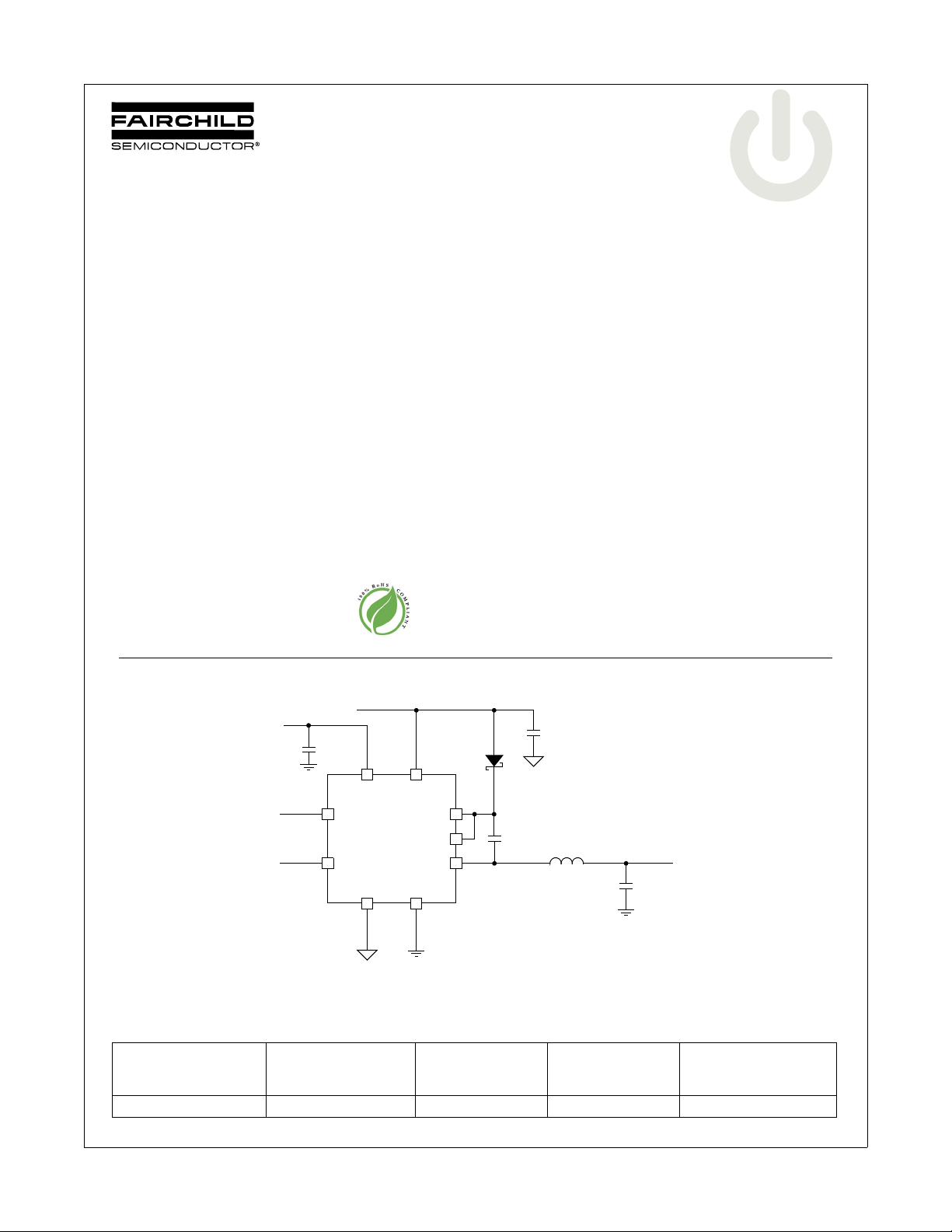
Powertrain Application Circuit
General Description
The FDMF8704 is a fully optimized integrated Driver plus
MOSFET power stage solution for high current synchronous
buck DC-DC applications. The device integrates a driver IC and
two Power MOSFETs into a space saving, MLP 8x8, 56-pin
package. Fairchild Semiconductor’s integrated approach
optimizes the complete switching power stage with regards to
driver to FET dynamic performance, system inductance and
overall solution ON resistance. Package parasitics and
problematical layouts associated with conventional discrete
solutions are greatly reduced. This integrated approach results
in significant board space saving, therefore maximizing footprint
power density. This solution is based on the Intel™ DrMOS
specification.
Applications
Desktop and server VR11.x V-core and non V-core buck
converters.
CPU/GPU power train in game consoles and high end
desktop systems.
High-current DC-DC Point of Load (POL) converters.
Networking and telecom microprocessor voltage regulators.
Small form factor voltage regulator modules.
7 - 20V
DISB
PWM
Input
5V
C
VIN
VIN VCIN
DISB
PWM
CGND PGND
C
VCIN
BOOT
HSEN
VSWH
Figure 1. Powertrain Application Circuit
C
BOOT
OUTPUT
C
OUT
Ordering Information
Current Rating
Max
Part
FDMF8704 32 12-19 1000 FDMF8704
[A]
Input Voltage
Typical
[V]
Frequency
Max
[KHz]
Device
Marking
©2007 Fairchild Semiconductor Corporation 1 www.fairchildsemi.com
FDMF8704 Rev. G
Page 2
Pin Configuration
PWM
DISB
NC
NC
NC
CGND
VSWH
VSWH
VSWH
VSWH
VSWH
VSWH
VSWH
VSWH
CGND
HSENNCVCIN
BOOT
CGNDNCVIN
VIN
TEST PAD 1
VIN
VIN
VIN
PGND
PGND
VIN
PGND
PGND
15
114
56
C
PGND
PGND
B
(VIN)
PGND
PGND
PGND
A
(CGND)
(VSWH)
43 28
42 29
VSWH
VSWH
PGND
VSWH
VIN
VIN
VIN
VIN
VIN
VIN
VSWH
PGND
PGND
PGND
PGND
PGND
PGND
PGND
FDMF8704 High Efficiency / High Frequency FET plus Driver Multi-chip Module
TEST PAD 2
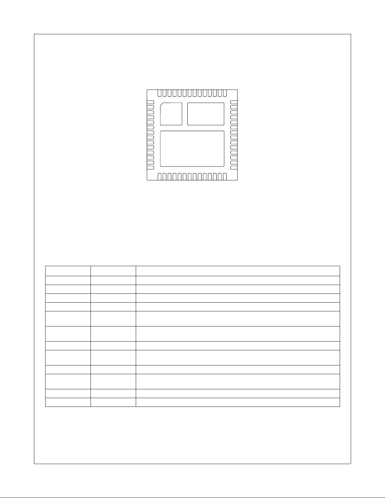
Figure 2. MLP 8x8 56L Bottom View
Pin Description
Pin Name Function
1, 6, 51, A CGND IC Ground. Ground return for driver IC.
2 HSEN High Side FET Enable. Must be connected to BOOT pin.
3, 7, 52-54 NC No connect
4 VCIN IC Supply. +5V chip bias power. Bypass with a 1µF ceramic capacitor.
5BOOT
21, 40-50, C VSWH
8, 9, 11-20, B VIN Power Input. Output stage supply voltage.
10 TEST PAD 1
22-38 PGND Power ground. Output stage ground. Source pin of low side MOSFET(s).
39 TEST PAD 2
55 DISB Output Disable. When low, this pin disable FET switching (HDRV and LDRV are held low).
56 PWM PWM Signal Input. This pin accepts a logic-level PWM signal from the controller.
Bootstrap Supply Input. Provides voltage supply to high-side MOSFET driver. Connect
bootstrap capacitor.
Switch Node Input. SW Provides return for high-side bootstrapped driver and acts as a
sense point for the adaptive shoot-thru protection.
For manufacturing test only. HDRV pin. This pin must be floated. Must not be connected to
any pin.
For manufacturing test only. LDRV pin. This pin must be floated. Must not be connected to
any pin.
FDMF8704 Rev. G
2 www.fairchildsemi.com
Page 3
Absolute Maximum Rating
Stresses exceeding the absolute maximum ratings may damage the device. The device may not function or be operable above the
recommended operating conditions and stressing the parts to these levels is not recommended. In addition, extended exposure to
stresses above the recommended operating conditions may affect device reliability. The absolute maximum ratings are stress ratings
only.
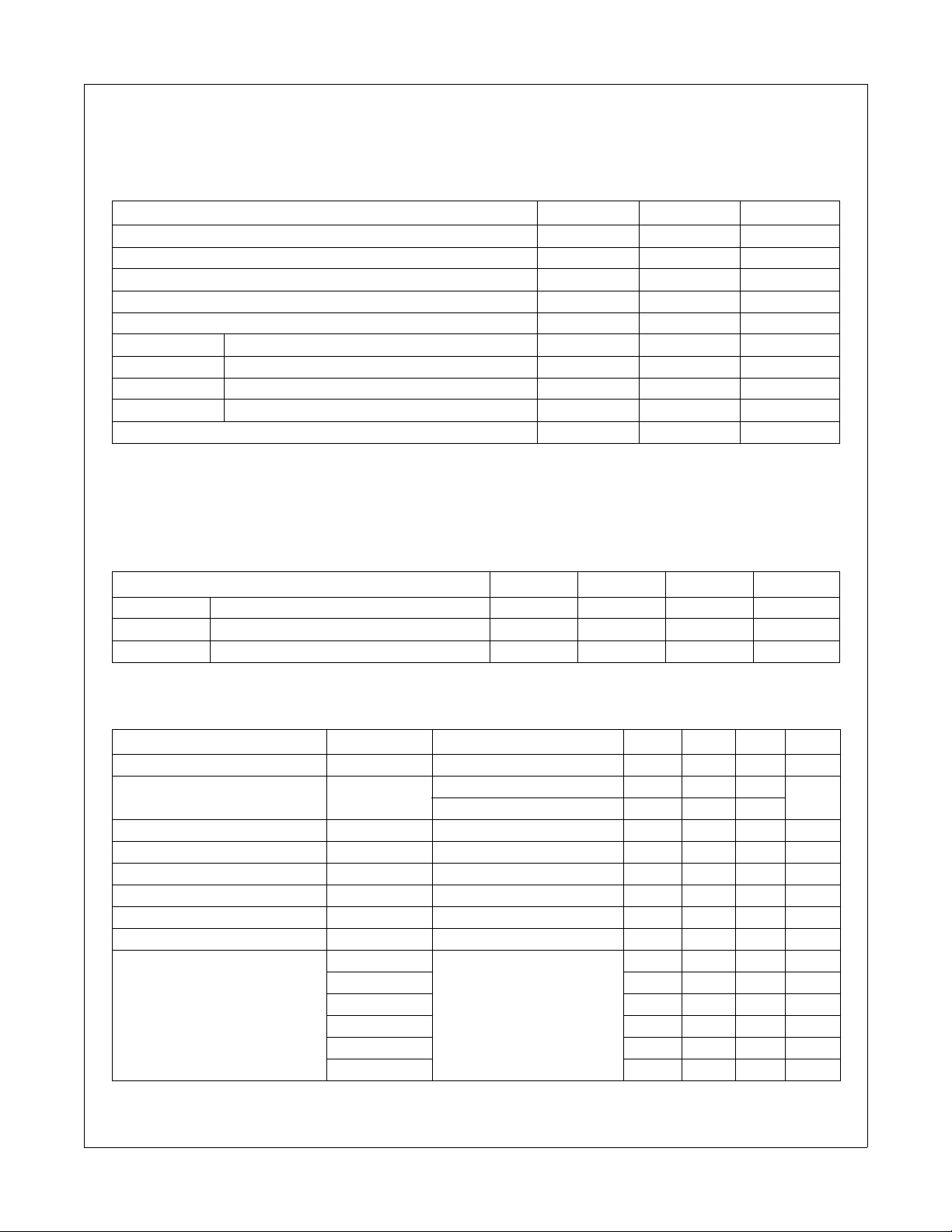
Parameter Min. Max. Units
V
, PWM, DISB to PGND -0.3 6 V
CIN
to PGND -0.3 24 V
V
IN
BOOT to VSWH -0.3 6 V
VSWH to PGND -1.0 24 V
BOOT to PGND -0.3 30 V
I
O(AV)
I
O(PK)
R
θJPCB
P
D
VIN = 12V, VO = 1.3V, fsw = 1MHz, T
VIN = 12V, t
= 10µs 65 A
PULSE
Junction to PCB Thermal Resistance (note 1) 5 °C/W
T
= 100°C (note 1) 10 W
PCB
Operating and Storage Junction Temperature Range -55 150 °C
Note 1: Package power dissipation based on 4 layers, 2 square inch, 2 oz. copper pad. R
thermal resistance with PCB temperature referenced at VSWH pin.
= 100°C 32 A
PCB
is the steady state junction to PCB
θJPCB
Recommended Operating Range
The Recommended Operating Conditions table defines the conditions for actual device operation. Recommended operating conditions are specified to ensure optimal performance to the datasheet specifications. Fairchild does not recommend exceeding them or
designing to Absolute Maximum Ratings.
FDMF8704 High Efficiency / High Frequency FET plus Driver Multi-chip Module
Parameter Min. Typ. Max. Units
V
V
V
CIN
IN
OUT
Control Circuit Supply Voltage 4.5 5 5.5 V
Output Stage Supply Voltage 7 12 20 V
Output Voltage 0.8 1.3 3.2 V
Electrical Characteristics
VIN = 12V, V
Parameter Symbol Conditions Min. Typ. Max. Units
Operating Voltage Range V
Control Circuit Supply Current I
PWM Input High Voltage V
PWM Input Low Voltage V
PWM Input Current I
DISB Input High Voltage V
DISB Input Low Voltage V
DISB Input Current I
Propagation Delay
Note 2: t
= 5V, TA = 25°C unless otherwise noted.
CIN
CC
IL(PWM)
IL(DISB)
t
PDL(DISB-LDRV)
t
PDH(DISB-LDRV)
t
PDL(LDRV)
t
PDL(HDRV)
t
PDH(LDRV)
t
PDH(HDRV)
PDL(LDRV/HRDV)
refers to HIGH-to-LOW transition, t
CIN
IH(PWM)
IL(PWM)
IHDISB)
IL(DISB)
4.5 5 5.5 V
fSW = 0Hz, V
= 1MHz, V
f
SW
= 0V 1 3
DISB
= 5V 50
DISB
mA
2.4 V
0.8 V
-2 2 µA
2.4 V
0.8 V
-2 2 µA
(2)
(2)
(2)
(2)
(2)
(2)
VIN = 12V, V
= 1MHz, IO = 30A
f
sw
PDH(LDRV/HDRV)
OUT
= 1.3V,
refers to LOW-to-HIGH transition.
8ns
6ns
9ns
22 ns
12 ns
20 ns
FDMF8704 Rev. G
3 www.fairchildsemi.com
Page 4
Functional Block Diagram
FDMF8704 High Efficiency / High Frequency FET plus Driver Multi-chip Module
VCIN
DISB
PWM
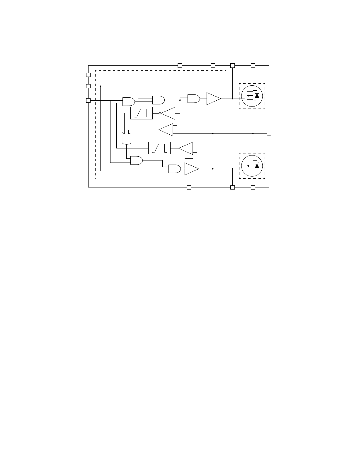
Figure 3. Functional Block Diagram
Functional Description
The FDMF8704 is a driver plus FET module optimized for
synchronous buck converter topology. A single PWM input
signal is all that is required to properly drive the high-side and
the low-side MOSFETs. Each part is capable of driving speeds
up to 1MHz.
Low-Side Driver
The low-side driver (LDRV) is designed to drive a ground
referenced low R
is internally connected between VCIN and CGND. When the
driver is enabled, the driver's output is 180° out of phase with
the PWM input. When the driver is disabled (DISB = 0V), LDRV
is held low.
High-Side Driver
The high-side driver (HDRV) is designed to drive a floating
N-channel MOSFET. The bias voltage for the high-side driver is
developed by a bootstrap supply circuit, consisting of the
external diode and external bootstrap capacitor (C
start-up, VSWH is held at PGND, allowing C
VCIN through the internal diode. When the PWM input goes
high, HDRV will begin to charge the high-side MOSFET's gate
(Q1). During this transition, charge is removed from C
delivered to Q1's gate. As Q1 turns on, VSWH rises to V
forcing the BOOT pin to V
sufficient VGS enhancement for Q1. To complete the switching
cycle, Q1 is turned off by pulling HDRV to VSWH. C
recharged to VCIN when VSWH falls to PGND. HDRV output is
in phase with the PWM input. When the driver is disabled, the
high-side gate is held low.
N-channel MOSFET. The bias for LDRV
DS(ON)
BOOT
IN
+V
, which provides
C(BOOT)
). During
BOOT
to charge to
and
BOOT
is then
BOOT
IN
HSEN
HDRV
VINBOOT
Q1
VSWH
Q2
VCIN
CGND
LDRV
PGND
Adaptive Gate Drive Circuit
The driver IC embodies an advanced design that ensures
minimum MOSFET dead-time while eliminating potential shootthrough (cross-conduction) currents. It senses the state of the
MOSFETs and adjusts the gate drive, adaptively, to ensure they
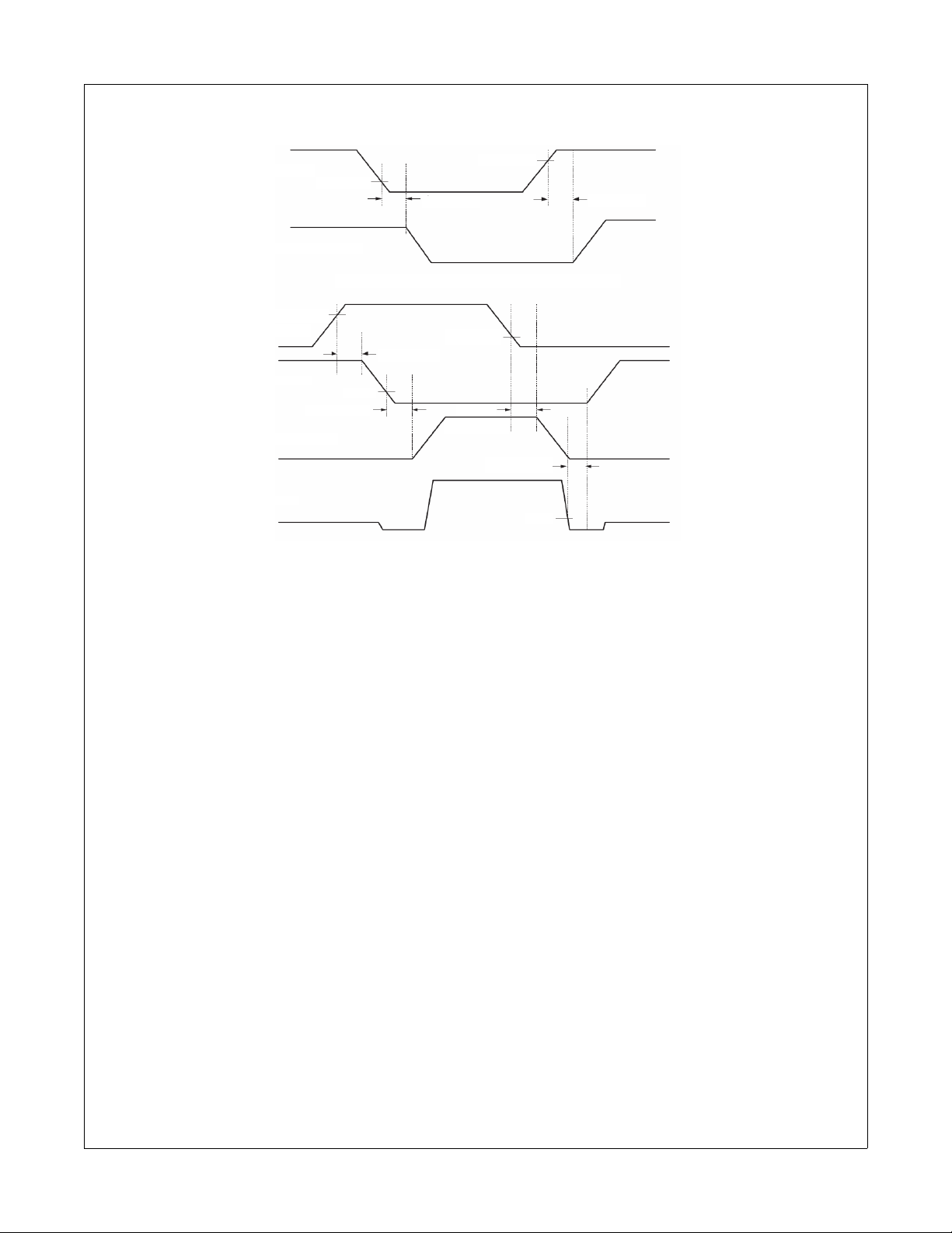
do not conduct simultaneously. Refer to Figure 4 and 5 for the
relevant timing waveforms. To prevent overlap during the lowto-high switching transition (Q2 OFF to Q1 ON), the adaptive
circuitry monitors the voltage at the LDRV pin. When the PWM
signal goes HIGH, Q2 will begin to turn OFF after some
propagation delay (t
discharged below ~1.2V, Q1 begins to turn ON after adaptive
delay t
PDH(HDRV)
PDL(LDRV)
. To preclude overlap during the high-to-low
transition (Q1 OFF to Q2 ON), the adaptive circuitry monitors
the voltage at the SW pin. When the PWM signal goes LOW, Q1
will begin to turn OFF after some propagation delay
(t
PDL(HDRV)
to turn ON after adaptive delay t
). Once the VSWH pin falls below ~2.2V, Q2 begins
Q1 is monitored. When V
secondary adaptive delay is initiated, which results in Q2 being
driven ON after t
function is implemented to ensure C
PDH(LDRV)
switching cycle, particularly for cases where the power
converter is sinking current and SW voltage does not fall below
the 2.2V adaptive threshold. Secondary delay t
longer than t
,
PDH(LDRV)
.
). Once the LDRV pin is
PDH(LDRV)
is discharged below ~1.2V, a
GS(Q1)
. Additionally, VGS of
, regardless of SW state. This
is recharged each
BOOT
PDH(HDRV)
is
FDMF8704 Rev. G
4 www.fairchildsemi.com
Page 5
Timing Diagram
DISB
V
IL(DISB)
LDRV / HDRV
V
IH(PWM)
PWM
LDRV
t
PDH(HDRV)
HDRV-SW
SW
t
PDL(DISB)
Figure 4. Output Disable Timing
V
IL(PWM)
t
PDL(LDRV)
1.2V
t
PDL(HDRV)
V
IH(DISB)
t
PDH(LDRV)
2.2V
t
PDH(DISB)
FDMF8704 High Efficiency / High Frequency FET plus Driver Multi-chip Module
Figure 5. Adaptive Gate Drive Timing
FDMF8704 Rev. G
5 www.fairchildsemi.com
Page 6
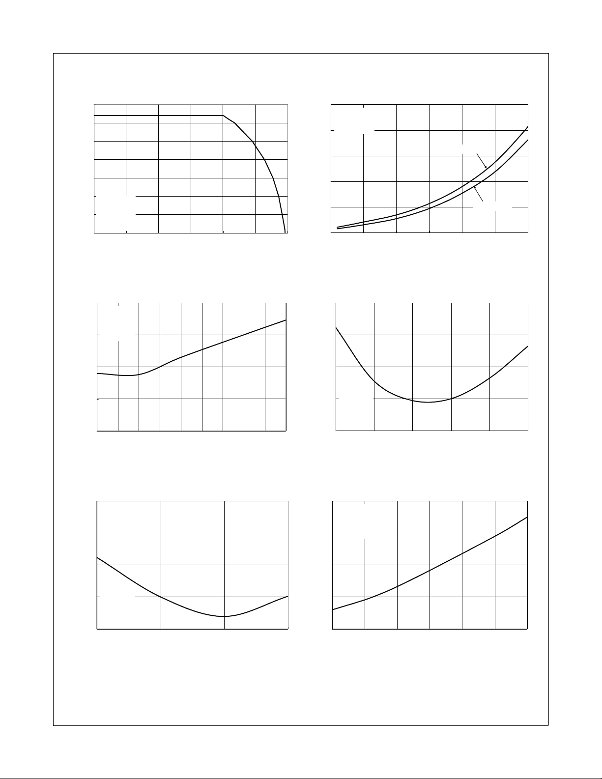
Typical Characteristics
0
0
0
6
VIN = 12V, V
35
30
25
20
, A
LOAD
I
15
10
5
0
0 25 50 75 100 125 15
= 5V, TA = 25°C unless otherwise noted.
CIN
VIN = 12V
= 1.3V
V
OUT
= 1MHz
f
SW
L = 0.33uH
PCB Temperature, oC
Figure 6. Safe Operating Area Figure 7. Module Power Loss vs. Output Current
10
VIN = 12V
= 1.3V
V
OUT
L = 0.33uH
8
6
fSW = 1MHz
, W
LOSS
P
4
2
fSW = 500KHz
0
0 5 10 15 20 25 3
I
LOAD
, A
FDMF8704 High Efficiency / High Frequency FET plus Driver Multi-chip Module
1.10
VIN = 12V
= 1.3V
V
OUT
= 30A
I
OUT
L = 0.33uH
1.00
0.90
(NORMALIZED)
LOSS
P
0.80
0.70
300 400 500 600 700 800 900 1000 1100 120
fSW, KHz
1.15
1.10
1.05
(NORMALIZED)
LOSS
P
V
= 1.3V
OUT
1.00
I
= 30A
OUT
L = 0.33uH
f
= 1MHz
SW
0.95
6 8 10 12 14 1
Input Voltage, V
Figure 8. Power Loss vs. Switching Frequency Figure 9. Power Loss vs. Input Voltage
1.15
1.10
1.05
(NORMALIZED)
VIN = 12V
LOSS
P
V
= 1.3V
OUT
1.00
I
= 30A
OUT
L = 0.33uH
f
= 1MHz
SW
0.95
4.5 5.0 5.5 6.0
Driver Supply Volt age, V
1.6
VIN = 12V
I
= 30A
OUT
L = 0.33uH
f
= 1MHz
SW
1.4
1.2
(NORMALIZED)
LOSS
P
1.0
0.8
0.8 1.2 1. 6 2.0 2.4 2.8 3.2
Output Voltage, V
Figure 10. Power Loss vs. Driver Supply Voltage Figure 11. Power Loss vs. Output Voltage
FDMF8704 Rev. G
6 www.fairchildsemi.com
Page 7
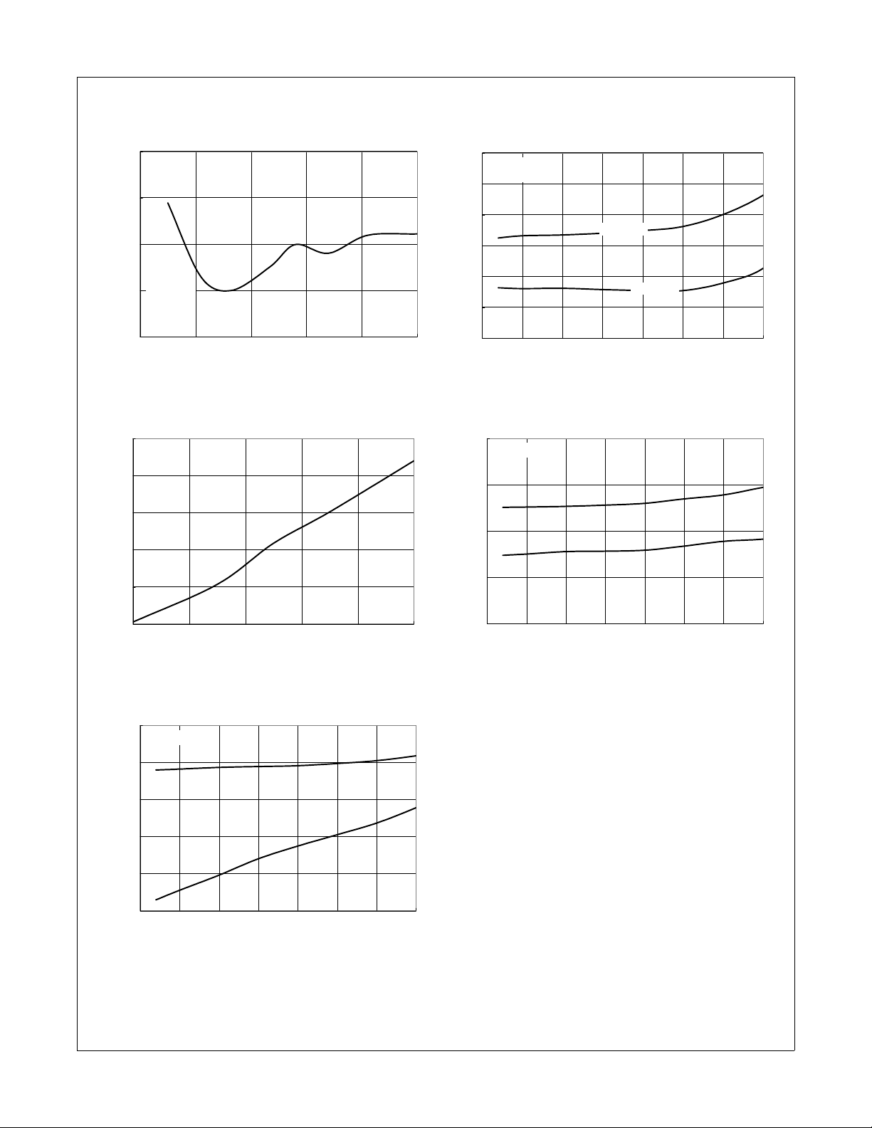
Typical Characteristics
0
V
V
VIN = 12V, V
1.06
1.04
1.02
(NORMALIZED)
LOSS
P
1.00
0.98
0.0 0.2 0.4 0.6 0.8 1. 0
= 5V, TA = 25°C unless otherwise noted.
CIN
VIN = 12V
V
= 1.3V
OUT
I
= 30A
OUT
f
= 1MHz
SW
Output Inductance, uH
Figure 12. Power Loss vs. Output Inductance Figure 13. Driver Supply Current vs. Temperature
1.0
V
= 5V
CIN
DISB = 5V
0.9
0.8
PWM = 5V
0.7
0.6
Driver Suppy Current , mA
PWM = 0V
0.5
0.4
-50 -25 0 25 50 75 100 125
Temperature,
o
C
FDMF8704 High Efficiency / High Frequency FET plus Driver Multi-chip Module
50
V
= 5V
CIN
40
1.83
1.81
V
= 5
CIN
V
IH
30
20
Driver Suppy Current , mA
10
0
0 200 400 600 800 100
fSW, KHz
1.79
1.77
PWM Threshold Voltage, V
1.75
-50 -25 0 25 50 75 100 125
V
IL
Temperature,
o
C
Figure 14. Driver Supply Current vs. Frequency Figure 15. PWM Threshold Voltage vs. Temperature
1.90
V
= 5
CIN
DISB Threshold Voltage, V
1.85
1.80
1.75
1.70
V
IH
V
IL
1.65
-50 -25 0 25 50 75 100 125
Temperature,
o
C
Figure 16. DISB Threshold Voltage vs. Temperature
7 www.fairchildsemi.com
FDMF8704 Rev. G
Page 8
FDMF8704 High Efficiency / High Frequency FET plus Driver Multi-chip Module
Application Information
Supply Capacitor Selection
For the supply input (V
bypass capacitor is recommended to reduce the noise and to
supply the peak current. Use at least a 1µF, X7R or X5R
capacitor. Keep this capacitor close to the FDMF8704 V
CGND pins.
) of the FDMF8704, a local ceramic
CIN
CIN
and
Bootstrap Circuit
The bootstrap circuit uses a charge storage capacitor (C
and the external schottky diode, as shown in Figure 18. A
BOOT
Typical Application
VIN 12V
V
5V
CIN
bootstrap capacitance of 100nF, X7R or X5R capacitor is
adequate.
The peak surge current rating of the boot diode should be
checked in-circuit, since this is dependent on the equivalent
impedance of the entire bootstrap circuit, including the PCB
traces. Boot diode must be sized big enough to carry the
forward charge current. Refer to Figure 14 for boot diode
average forward current.
The bootstrap diode must have low V
)
leakage. Breakdown voltage of the bootstrap diode must be
greater than the BOOT to VSWH voltage.
VIN VCIN
PWM
PWM
DISB
CGND PGND
BOOT
HSEN
VSWH
FDMF8704
and low reverse current
F
VCC
PWM
Controller
GND
Signal
GND
EN
PWM1
PWM2
PWM3
PWM4
Power
GND
VIN VCIN
PWM
DISB
CGND PGND
VIN VCIN
PWM
DISB
CGND PGND
VIN VCIN
PWM
DISB
CGND PGND
BOOT
HSEN
VSWH
BOOT
HSEN
VSWH
BOOT
HSEN
VSWH
FDMF8704
VOUT
FDMF8704
FDMF8704
FDMF8704 Rev. G
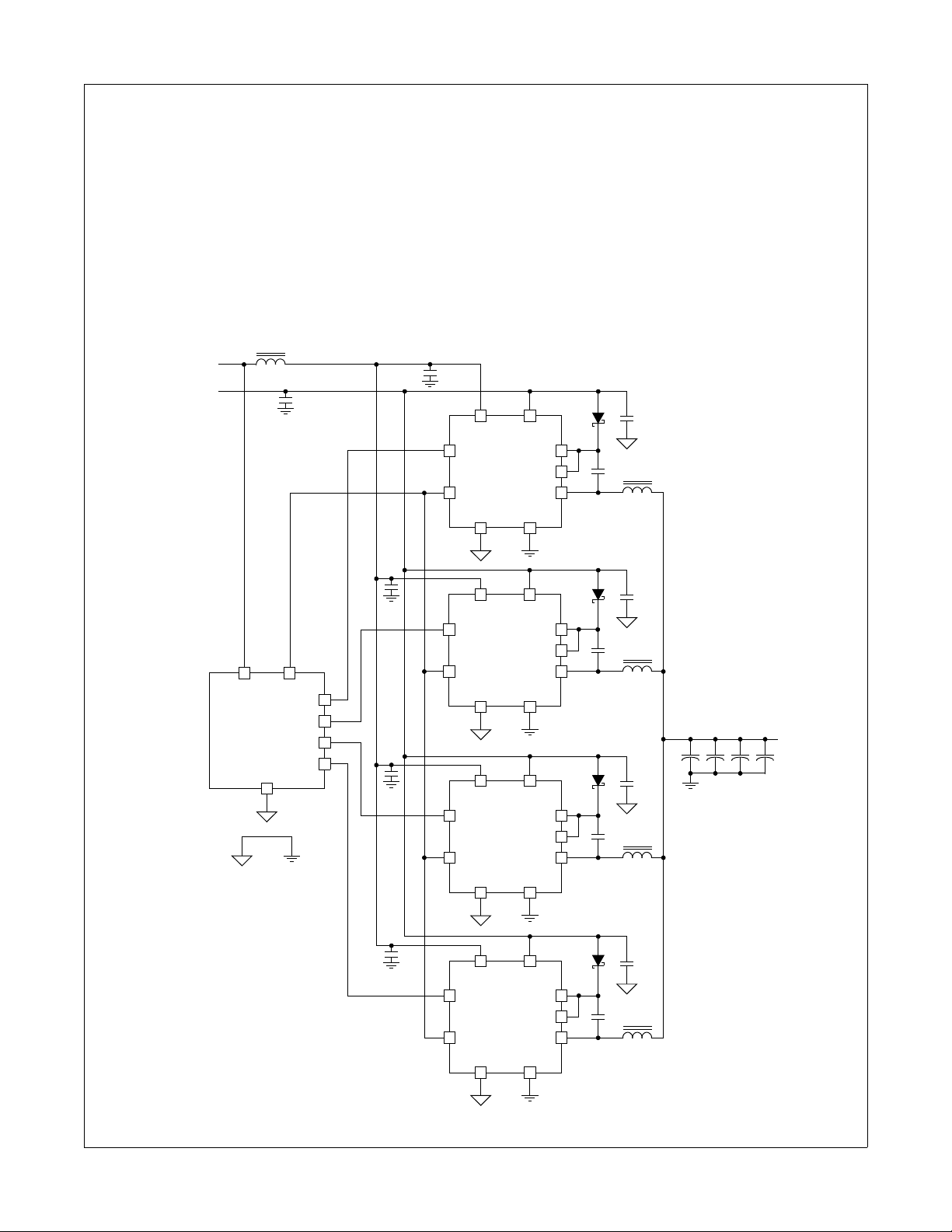
Figure 17. Typical Application
8 www.fairchildsemi.com
Page 9
FDMF8704 High Efficiency / High Frequency FET plus Driver Multi-chip Module
Module Power Loss Measurement and
Calculation
Refer to Figure 18 for module power loss testing method. Power
loss calculation are as follows:
(a) P
= (VIN x IIN) + (V
IN
(b) P
(c) P
= VO x I
OUT
= PIN - P
LOSS
OUT
OUT
(W)
(W)
CIN
x I
CIN
) (W)
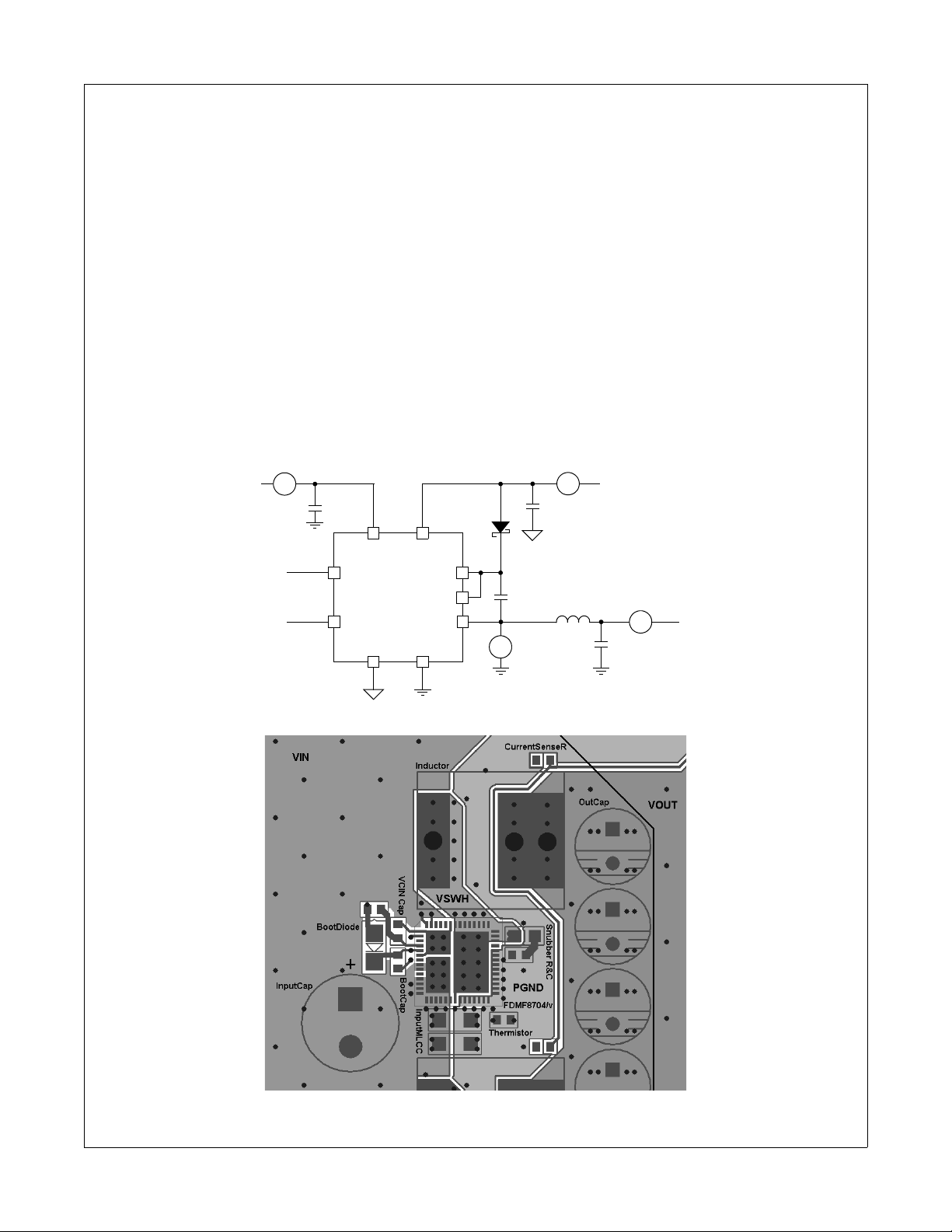
PCB Layout Guideline
Figure 19. shows a proper layout example of FDMF8704 and
critical parts. All of high current flow path, such as V
V
and GND copper, should be short and wide for better and
OUT
stable current flow, heat radiation and system performance.
Following is a guideline which the PCB designer should
consider:
1. Input bypass capacitors should be close to V
of FDMF8704 to help reduce input current ripple component
induced by switching operation.
I
IN
V
A
IN
C
VIN
VIN VCIN
DISB
PWM
Input
DISB
PWM
CGND PGND
, VSWH,
IN
and GND pin
IN
BOOT
HSEN
VSWH
2. It is critical that the VSWH copper has minimum area for
lower switching noise emission. VSWH copper trace should
also be wide enough for high current flow. Other signal routing
path, such as PWM IN and BOOT signal, should be considered
with care to avoid noise pickup from VSWH copper area.
3. Output inductor location should be as close as possible to the
FDMF8704 for lower power loss due to copper trace.
4. Snubber for suppressing ringing and spiking of VSWH
voltage should be placed near the FDMF8704. The resistor and
capacitor need to be of proper size for power dissipation.
5. Place boot diode, ceramic bypass capacitor and boot
capacitor as close to V
and BOOT pin of FDMF8704 in order
CIN
to supply stable power. Routing width and length should also be
considered
6. Use multiple Vias on each copper area to interconnect each
top, inner and bottom layer to help smooth current flow and heat
conduction. Vias should be relatively large and of reasonable
inductance.
I
CIN
A
V
CIN
C
VCIN
C
BOOT
V
V
O
L
I
OUT
A
C
OUT
V
OUT
Figure 18. Power Loss Measurement Block Diagram
Figure 19. Typical PCB Layout Example (Top View)
FDMF8704 Rev. G
9 www.fairchildsemi.com
Page 10
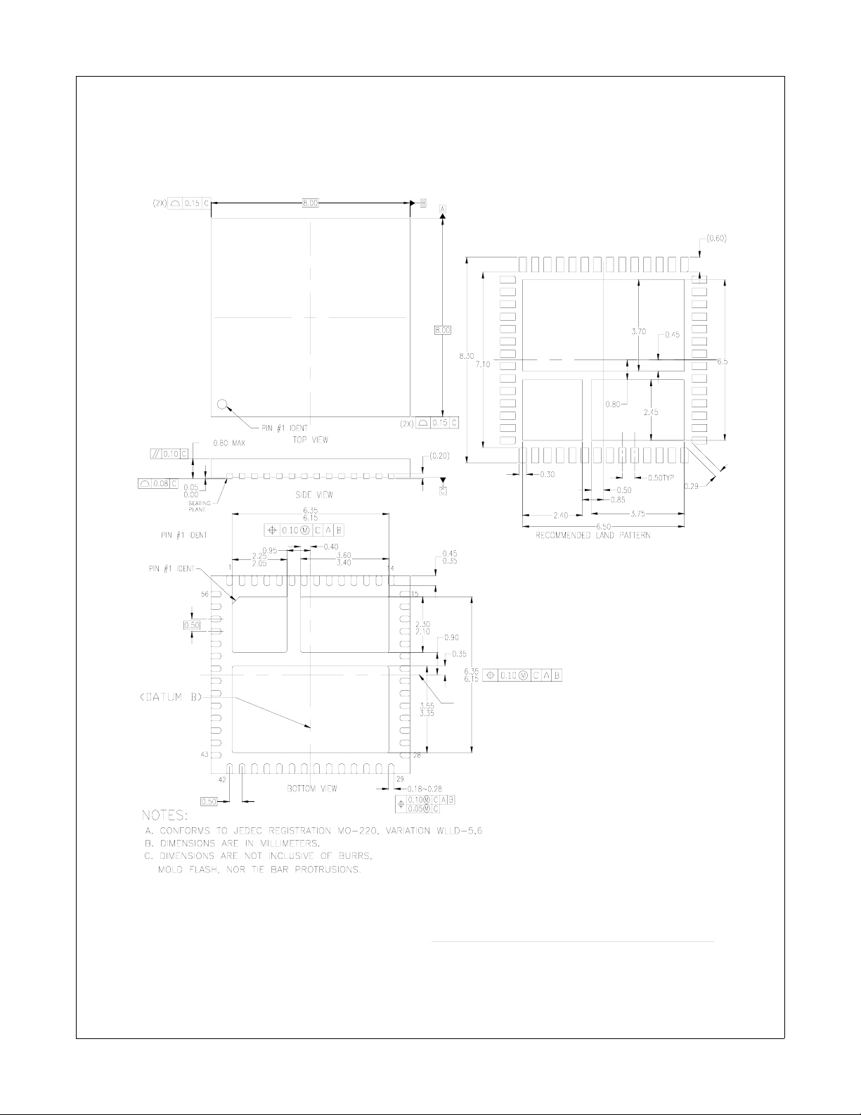
Dimensional Outline and Pad layout
FDMF8704 High Efficiency / High Frequency FET plus Driver Multi-chip Module
FDMF8704 Rev. G
(DATUM A)
Bayan Lepas FIZ
11900, Penang, Malaysia
10 www.fairchildsemi.com
Page 11
TRADEMARKS
The following includes registered and unregistered trademarks and service marks, owned by Fairchild Semiconductor and/or its global
subsidiaries, and is not intended to be an exhaustive list of all such trademarks.
®
ACEx
Build it Now™
CorePLUS™
CROSSVOLT™
CTL™
Current Transfer Logic™
EcoSPARK
®
EZSWITCH™ *
™
®
®
Fairchild
Fairchild Semiconduct or
FACT Quiet Series™
FACT
FAST
FastvCore™
FlashWriter
®
®
® *
®
* EZSWITCH™ and FlashWriter
FPS™
®
FRFET
Global Power ResourceSM
Green FPS™
Green FPS™ e-Series™
GTO™
i-Lo™
IntelliMAX™
ISOPLANAR™
MegaBuck™
MICROCOUPLER™
MicroFET™
MicroPak™
MillerDrive™
Motion-SPM™
OPTOLOGIC
OPTOPLANAR
®
®
are trademarks of System General Corporation, used under license by Fairchild Semiconductor.
®
®
PDP-SPM™
Power220
Power247
POWEREDGE
Power-SPM™
PowerTrench
Programmable Active Droop™
QFET
®
®
®
®
®
QS™
QT Optoelectronics™
Quiet Series™
RapidConfigure™
SMART START™
®
SPM
STEALTH™
SuperFET™
SuperSOT™-3
SuperSOT™-6
SuperSOT™-8
SyncFET™
The Power Franchise
®
TinyBoost™
TinyBuck™
TinyLogic
TINYOPTO™
TinyPower™
TinyPWM™
TinyWire™
μSerDes™
UHC
Ultra FRFET™
UniFET™
VCX™
®
®
DISCLAIMER
FAIRCHILD SEMICONDUCTOR RESERVES THE RIGHT TO MAKE CHANGES WITHOUT FURTHER NOTICE TO ANY PR ODUCTS
HEREIN TO IMPROVE RELIABILITY, FUNCTION, OR DESIGN. FAIRCHILD DOES NOT ASSUME ANY LIABILITY ARISING OUT OF THE
APPLICATION OR USE OF AN Y PRODUCT OR CIRCUIT DESCRIBED HEREIN; NEITHER DOES IT CONVEY ANY LICENSE UNDER ITS
PATENT RIGHTS, NOR THE RIG HTS OF OTH ERS. THESE SPECIFICATIO NS DO N OT EXPAN D THE TERM S OF FAIRCHILD’S
WORLDWIDE TERMS AND CONDITIONS, SPECIFIC ALLY THE WARRANTY THER EIN, WHICH COVERS TH ESE PRODUCTS.
LIFE SUPPORT POLICY
FAIRCHILD’S PRODUCTS ARE NOT AUTHORIZED FOR USE AS CRITICAL COMPONENTS IN LIFE SUPPORT DEVICES OR
SYSTEMS WITHOUT THE EXPRESS WRITTEN APPROVAL OF FAIRCHILD SEMICONDUCTOR CORPORATION.
As used herein:
1. Life support devices or systems are devices or systems
which, (a) are intended for surgical im plant into the body or
(b) support or sustain lif e, and (c) whose failure to perform
when properly used in accordance with instructi ons for use
2. A critical component in any component of a life support,
device, or system whose failure to perform can be
reasonably expected to cause the fail ure of the life support
device or system, or to affect its s afety or effectiveness.
provided in the labeling, can be reasonably expected to
result in a signific ant injury of the user.
PRODUCT STATUS DEFINITIONS
Definition of Terms
Datasheet Identification Product Status Definition
Advance Information Formative or In Design
Preliminary First Production
No Identification Needed Ful l Production
Obsolete Not In Production
This datasheet contains the design specificati ons for product
development. Specif i cations may change in any manner without notice.
This datasheet contains prelim inary data; supplementary data will be
published at a later date. Fairc hi l d Semiconductor reserves the right to
make changes at any ti me without notice to improve design.
This datasheet contains final specifications. Fairchild Semic onduc tor
reserves the right to make changes at any time without notice to improve
the design.
This datasheet contains specifications on a product that has been
discontinued by Fairchild Semiconductor. The datasheet i s printed for
reference information only.
Rev. I32
®
© 2007 Fairchild Semiconductor Corporation www.fairchildsemi.com
 Loading...