

Page 1
March 2012
FDMF6705V - Extra-Small, High-Performance, HighFrequency DrMOS Module
Benefits
Single 12V Input Power Supply Operation
Ultra-Compact 6x6mm PQFN, 72% Space-Saving
Compared to Conventional Discrete Solutions
Fully Optimized System Efficiency
Clean Switching Waveforms with Minimal Ringing
High-Current Handling
Features
Over 93% Peak-Efficiency
High-Current Handling of 43A
High-Performance PQFN Copper Clip Package
3-State 5V PWM Input Driver
Shorter Propagation Delays than FDMF6704V
Shorter Dead Times than FDMF6704V
Skip-Mode SMOD# (Low-Side Gate Turn Off) Input
Thermal Warning Flag for Over-Temperature
Condition
Driver Output Disable Function (DISB# Pin)
Internal Pull-Up and Pull-Down for SMOD# and
DISB# Inputs, Respectively
Fairchild PowerTrench® Technology MOSFETs for
Clean Voltage Waveforms and Reduced Ringing
Fairchild SyncFET™ (Integrated Schottky Diode)
Technology in the Low-Side MOSFET
Integrated Bootstrap Schottky Diode
Adaptive Gate Drive Timing for Shoot-through
Protection
Under-Voltage Lockout (UVLO)
Optimized for Switching Frequencies up to 1MHz
Low-Profile SMD Package
Fairchild Green Packaging and RoHS Compliant
Based on the Intel® 4.0 DrMOS Standard
Description
The XS™ DrMOS family is Fairchild’s next-generation,
fully optimized, ultra-compact, integrated MOSFET
plus driver power stage solutions for high-current,
high-frequency, synchronous buck DC-DC
applications. The FDMF6705V integrates a driver IC,
two power MOSFETs, and a bootstrap Schottky diode
into a thermally enhanced, ultra-compact 6x6mm
PQFN package.
With an integrated approach, the complete switching
power stage is optimized with regards to driver and
MOSFET dynamic performance, system inductance,
and Power MOSFET R
Fairchild's high-performance PowerTrench® MOSFET
technology, which dramatically reduces switch ringing,
eliminating the need for a snubber circuit in most buck
converter applications.
A new driver IC with reduced dead times and
propagation delays further enhances the performance of
this part. A thermal warning function has been included
to warn of a potential over-temperature situation. The
FDMF6705V also incorporates features, such as Skip
Mode (SMOD), for improved light-load efficiency along
with a 3-state PWM input for compatibility with a wide
range of PWM controllers.
. XS™ DrMOS uses
DS(ON)
Applications
High-Performance Gaming Motherboards
Compact Blade Servers, V-Core and Non-V-Core
DC-DC Converters
Desktop Computers, V-Core and Non-V-Core
DC-DC Converters
Workstations
High-Current DC-DC Point-of-Load (POL)
Converters
Networking and Telecom Microprocessor Voltage
Regulators
Small Form-Factor Voltage Regulator Modules
FDMF6705V - Extra-Small High-Performance, High-Frequency DrMOS Module
Ordering Information
Part
Number
FDMF6705V 40A 12V 1000kHz
© 2011 Fairchild Semiconductor Corporation www.fairchildsemi.com
FDMF6705V • Rev. 1.0 2
Current
Rating
Input
Voltage
Switching
Frequency
Package Top Mark
40-Lead, Clipbond PQFN DrMOS,
6.0x6.0mm Package
FDMF6705V
Page 2
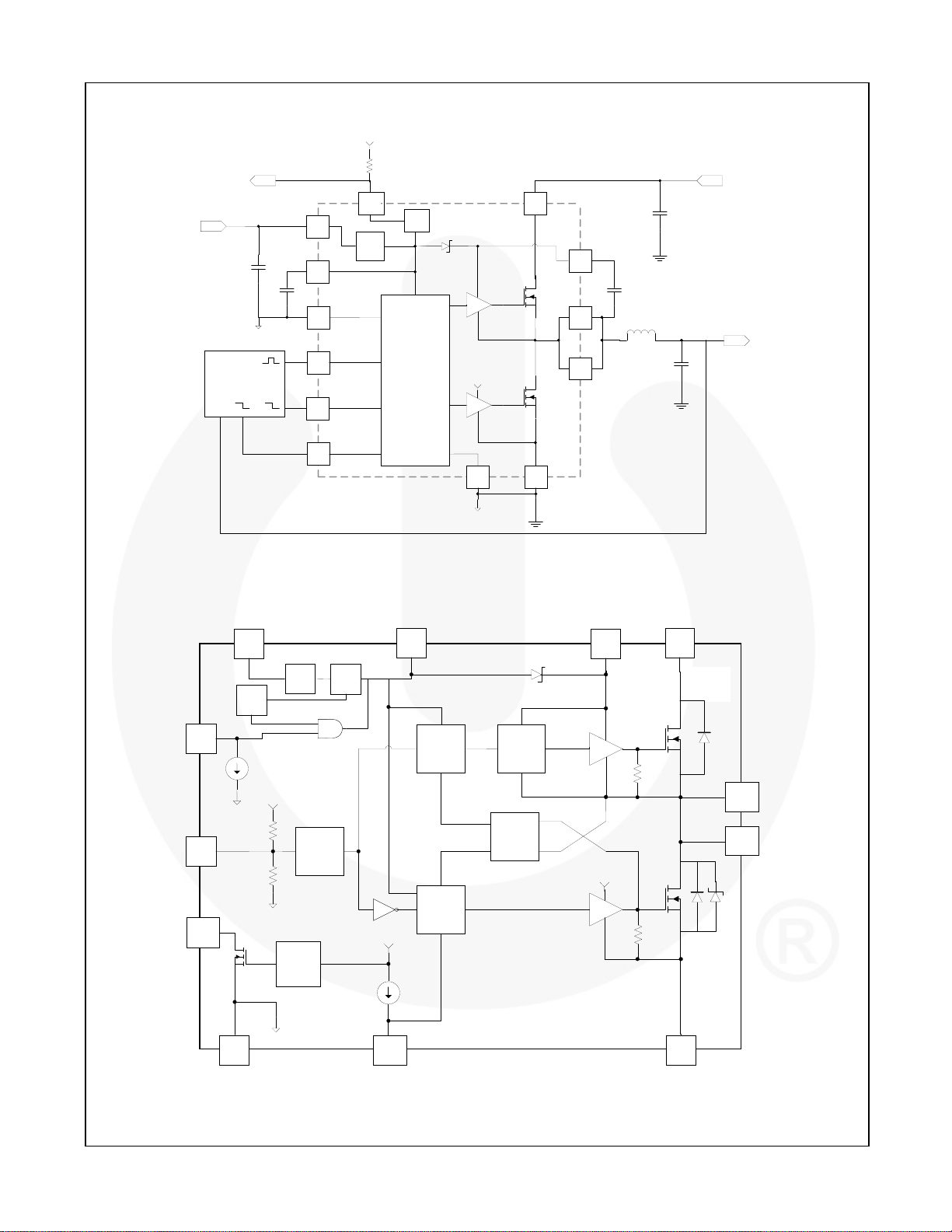
Typical Application Circuit
t
V
FDMF6705V - Extra-Small High-Performance, High-Frequency DrMOS Module
V
CIN
V
=3V to15 V
IN
V
DRV
=8V to 15 V
C
VDRV
C
VCI
PWM
Control
Enable
OFF
Disabled ON
DrMOS Block Diagram
VDRV VIN
THWN#
VDRV
VCIN
CGND
PWM
SMOD #
DISB #
5
Linear
Reg
Temp
Sense
.
Control
D
Boo
HDRV
V
CIN
LDRV
CGND
Figure 1. Typical Application Circuit
VCIN
VIN
PGND
C
VIN
BOOT
Q1
PHASE
VSWH
L
OUT
C
OUT
V
OUT
Q2
BOOT
GL
30kΩ
30kΩ
PGND
Q1
HS Power
MOSFET
Q2
LS Power
MOSFET
PHASE
VSWH
DISB#
PWM
THWN#
VCC
UVLO
R
R
DN_PWM
CGND
UP_PWM
10µA
V
VIN
UVLO
CIN
Temp.
Sense
Input
-State
3
Logic
5V
LDO
V
CIN
SMOD#
10µA
GH
Logic
GL
Logic
Level Shift
Dead-Time
Control
D
Boot
GH
V
CIN
Figure 2. DrMOS Block Diagram
© 2011 Fairchild Semiconductor Corporation www.fairchildsemi.com
FDMF6705V • Rev. 1.0.2 2
Page 3
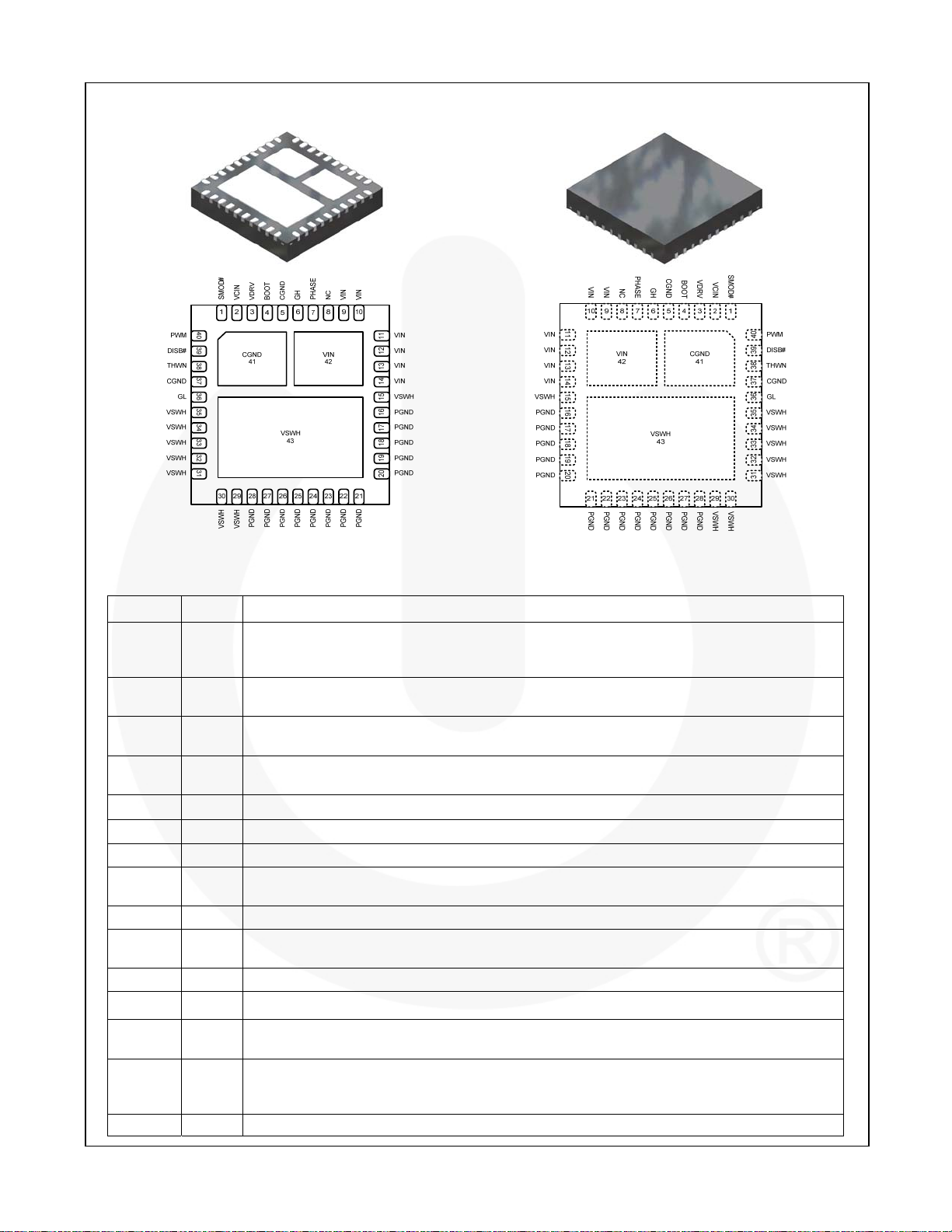
Pin Configuration
FDMF6705V - Extra-Small High-Performance, High-Frequency DrMOS Module
Figure 3. Bottom View Figure 4. Top View
Pin Definitions
Pin # Name Description
When SMOD#=HIGH, the low-side driver is the inverse of PWM input. When SMOD#=LOW,
1 SMOD#
2 VCIN
3 VDRV
4 BOOT
5, 37, 41 CGND IC ground. Ground return for driver IC.
6 GH For manufacturing test only. This pin must float. Must not be connected to any pin.
7 PHASE Switch node pin for bootstrap capacitor routing. Electrically shorted to VSWH pin.
8 NC
9 - 14, 42 VIN Power input. Output stage supply voltage.
15, 29 -
35, 43
16 – 28 PGND Power ground. Output stage ground. Source pin of low-side MOSFET.
36 GL For manufacturing test only. This pin must float. Must not be connected to any pin.
38 THWN#
39 DISB#
40 PWM
VSWH
the low-side driver is disabled. This pin has a 10µA internal pull-up current source. Do not add a
noise filter capacitor.
Linear regulator 5V output. IC bias supply for gate drive output stage. Minimum 1µF ceramic
capacitor is required and should be connected as close as possible from this pin to CGND
Linear regulator input. Minimum 1µF ceramic capacitor is recommended and should be
connected as close as possible from this pin to CGND.
Bootstrap supply input. Provides voltage supply to high-side MOSFET driver. Connect
bootstrap capacitor from this pin to PHASE.
No connect. The pin is not electrically connected internally, but can be connected to VIN for
convenience.
Switch node input. Provides return for high-side bootstrapped driver and acts as a sense point
for the adaptive shoot-through protection.
Thermal warning flag, open collector output. When temperature exceeds the trip limit, the
output is pulled LOW. THWN# does not disable the module.
Output disable. When LOW, this pin disables Power MOSFET switching (GH and GL are held
LOW). This pin has a 10µA internal pull-down current source. Do not add a noise filter
capacitor.
PWM signal input. This pin accepts a 3-state logic-level PWM signal from the controller.
© 2011 Fairchild Semiconductor Corporation www.fairchildsemi.com
FDMF6705V • Rev. 1.0.2 3
Page 4
FDMF6705V - Extra-Small High-Performance, High-Frequency DrMOS Module
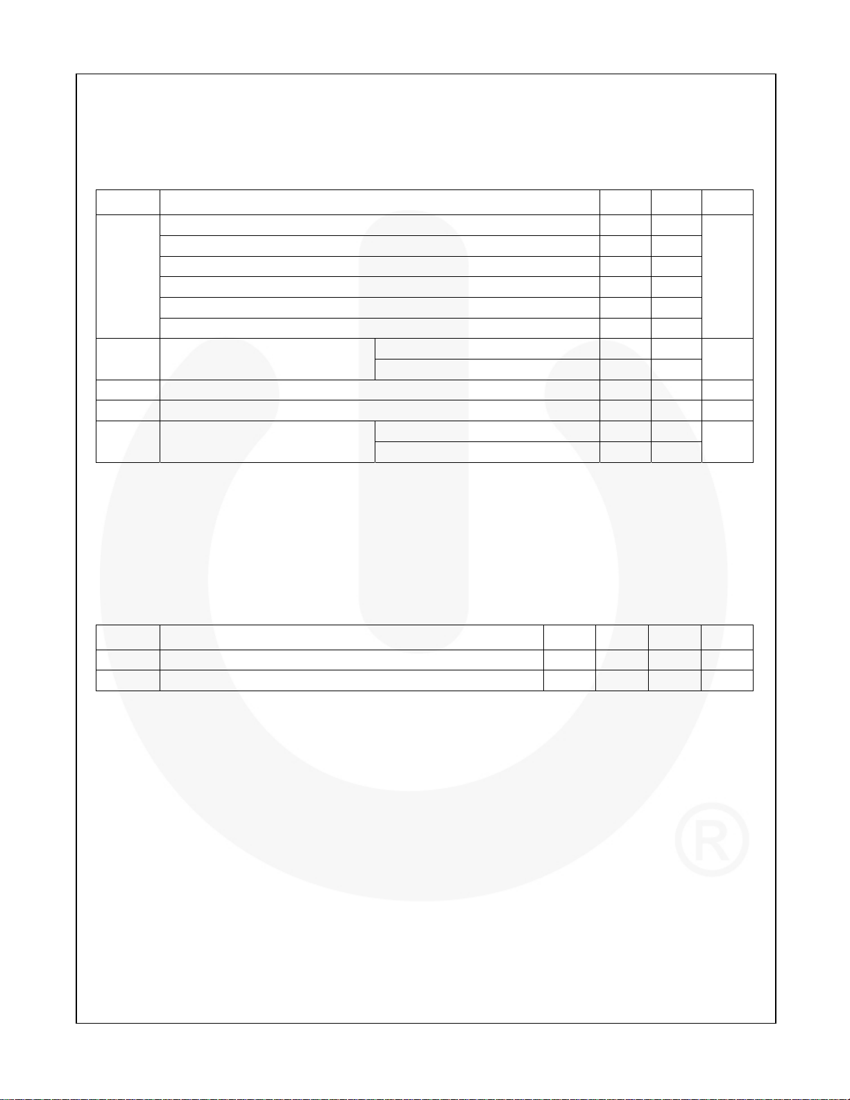
Absolute Maximum Ratings
Stresses exceeding the absolute maximum ratings may damage the device. The device may not function or be
operable above the recommended operating conditions and stressing the parts to these levels is not recommended.
In addition, extended exposure to stresses above the recommended operating conditions may affect device reliability.
The absolute maximum ratings are stress ratings only.
Symbol Parameter Min. Max. Unit
VCIN, DISB#, PWM, SMOD#, GL, THWN# to CGND Pins 6
VIN to PGND, CGND Pins 25
VDRV to PGND, CGND 16
BOOT, GH to VSWH, PHASE Pins 6
BOOT, VSWH, PHASE, GH to GND Pins 25
BOOT to VCIN Pins 22
f
=300kHz 43
(1)
I
O(AV)
θ
T
JPCB
STG
=12V, VO=1.0V
VIN
Junction-to-PCB Thermal Resistance 3.5 °C/W
Operating and Storage Temperature Range -55 +150 °C
ESD Electrostatic Discharge Protection
SW
fSW=1MHz 40
Human Body Model, JESD22-A114 2000
Charged Device Model, JESD22-C101 2000
Note:
1. I
is rated using Fairchild’s DrMOS evaluation board, TA = 25°C, natural convection cooling. This rating is limited
O(AV)
by the peak DrMOS temperature, T
= 150°C, and varies depending on operating conditions and PCB layout. This
J
rating can be changed with different application settings.
V
A
V
Recommended Operating Conditions
The Recommended Operating Conditions table defines the conditions for actual device operation. Recommended
operating conditions are specified to ensure optimal performance to the datasheet specifications. Fairchild does not
recommend exceeding them or designing to Absolute Maximum Ratings.
Symbol Parameter Min. Typ. Max. Unit
V
Gate Drive Control Circuit Input Supply Voltage
DRV
VIN Output Stage Supply Voltage
(2)
Note:
2. Operating at high V
can create excessive AC overshoots on the VSWH-to-GND and BOOT-to-GND nodes
IN
during MOSFET switching transients. For reliable DrMOS operation, VSWH-to-GND and BOOT-to-GND must
remain at or below the Absolute Maximum Ratings shown in the table above. Refer to the “Application
Information” and “PCB Layout Guidelines” sections of this datasheet for additional information.
8 12 15
3 12 15
V
V
© 2011 Fairchild Semiconductor Corporation www.fairchildsemi.com
FDMF6705V • Rev. 1.0.2 4
Page 5
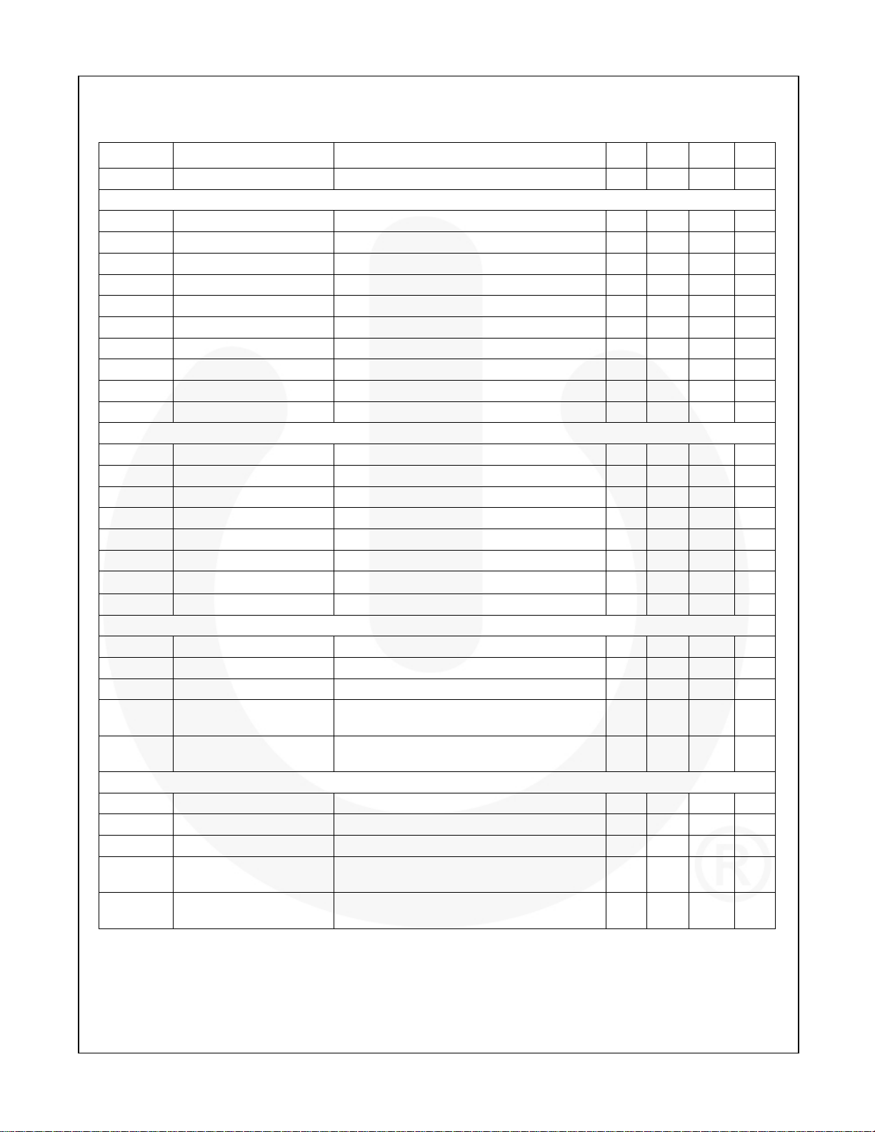
Electrical Characteristics
Typical values are VIN=12V, V
Symbol Parameter Condition Min. Typ. Max. Unit
I
Operating Current V
DRV
Internal 5V Linear Regulator
V
Input Voltage 8 12 14 V
DRV
I
Input Current 8V<VIN<14V, fSW=1MHz 36 mA
DRV
V
Output Voltage V
CIN
P
Power Dissipation V
VDRV
C
VCIN Bypass Capacitor X7R or X5R Ceramic 1 10 µF
VCIN
V
Line Regulation 8V<VIN<14V, I
RLINE
V
Load Regulation V
RLOAD
Short-Circuit Current Limit 200 mA
UVLO UVLO Threshold V
UVLO
PWM Input
R
UP_PWM
R
Down_PWM
V
V
V
V
t
D_HOLD-OFF
V
HiZ_PWM
DISB# Input
V
V
t
PD_DISBL
t
PD_DISBH
SMOD# Input
V
IH_SMOD
V
IL_SMOD
t
PD_SLGLL
t
PD_SHGLH
UVLO Hysteresis 0.435 V
_Hyst
Pull-Up Impedance 10 kΩ
Pull-Down Impedance 10 kΩ
PWM High Level Voltage 3.30 3.55 3.80 V
IH_PWM
3-State Rising Threshold 3.20 3.45 3.70 V
TRI_HI
3-State Falling Threshold 1.00 1.25 1.50 V
TRI_LO
PWM Low Level Voltage 0.85 1.15 1.40 V
IL_PWM
3-State Shutoff Time 160 200 ns
3-State Open Voltage 2.3 2.5 2.7 V
High-Level Input Voltage 2 V
IH_DISB
Low-Level Input Voltage 0.8 V
IL_DISB
I
Pull-Down Current 10 µA
PLD
Propagation Delay
Propagation Delay
High-Level Input Voltage 2 V
Low-Level Input Voltage 0.8 V
I
Pull-Up Current 10 µA
PLM
Propagation Delay
Propagation Delay
=12V, and TA=+25°C unless otherwise noted.
DRV
=14V, PWM=LOW or HIGH or Float 2 5 mA
DRV
=8V, I
DRV
=12V, fSW=1MHz 250 mW
DRV
=8V, 5mA<I
DRV
Rising 6.8 7.3 7.8 V
DRV
=5mA 4.8 5.0 5.2 V
LOAD
=5mA 20 mV
LOAD
<100mA 75 mV
LOAD
PWM=GND, Delay Between DISB# from
HIGH to LOW to GL from HIGH to LOW
PWM=GND, Delay Between DISB# from
LOW to HIGH to GL from LOW to HIGH
PWM=GND, Delay Between SMOD# from
HIGH to LOW to GL from HIGH to LOW
PWM=GND, Delay Between SMOD# from
LOW to HIGH to GL from LOW to HIGH
25 ns
25 ns
10 ns
10 ns
Continued on the following page…
FDMF6705V - Extra-Small High-Performance, High-Frequency DrMOS Module
© 2011 Fairchild Semiconductor Corporation www.fairchildsemi.com
FDMF6705V • Rev. 1.0.2 5
Page 6
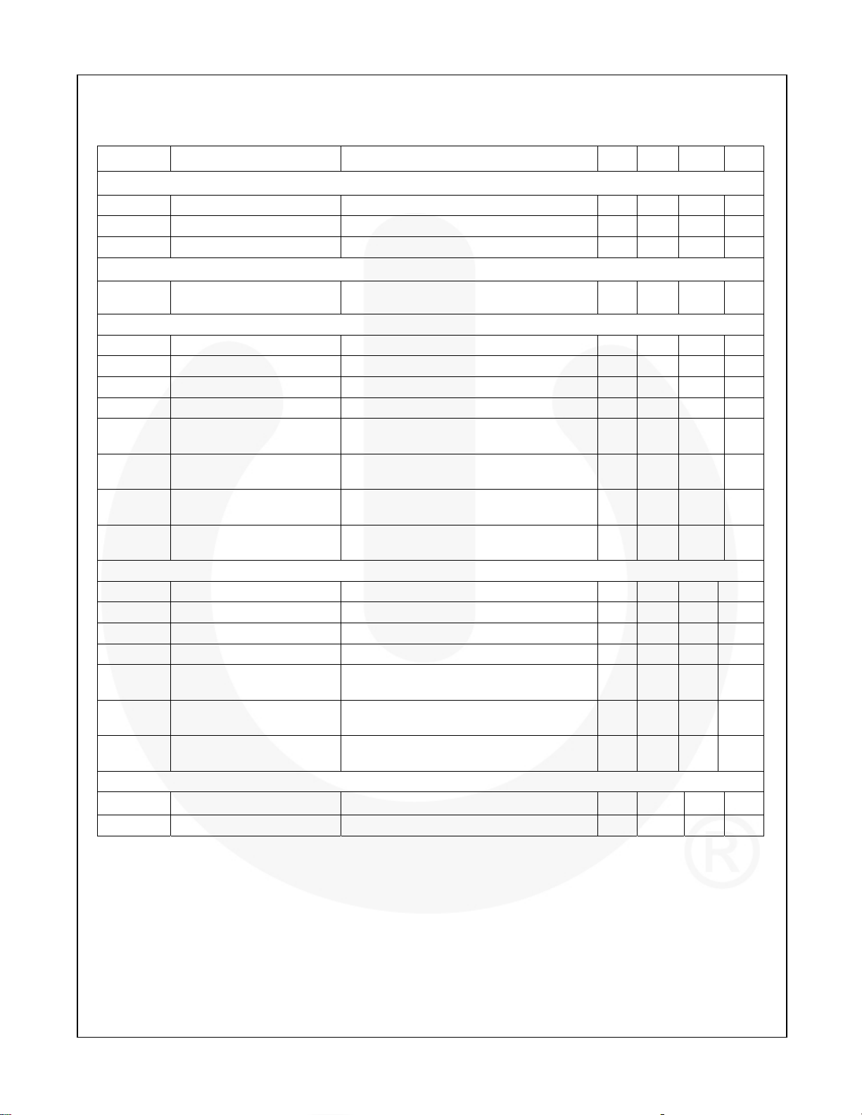
Electrical Characteristics (Continued)
Typical values are VIN=12V, V
Symbol Parameter Condition Min. Typ. Max. Unit
Thermal Warning Flag
T
Activation Temperature 150 °C
ACT
T
Reset Temperature 135 °C
RST
R
Pull-Down Resistance I
THWN
250ns Timeout Circuit
t
D_TIMEOUT
High-Side Driver
R
SOURCE_GH
R
t
D_DEADON
t
PD_PLGHL
t
PD_PHGHH
t
PD_TSGHH
Low-Side Driver
R
SOURCE_GL
R
t
D_DEADOFF
t
PD_PHGLL
t
PD_TSGLH
Boot Diode
Timeout Delay
Output Impedance, Sourcing Source Current=100mA 1 Ω
SINK_GH
t
R_GH
t
F_GH
SINK_GL
t
R_GL
t
F_GL
VF
VR
Output Impedance, Sinking Sink Current=100mA 0.8 Ω
Rise Time GH=10% to 90%, C
Fall Time GH=90% to 10%, C
LS to HS Deadband Time
PWM LOW Propagation
Delay
PWM HIGH Propagation
Delay (SMOD Held LOW)
Exiting 3-State Propagation
Delay
Output Impedance, Sourcing Source Current=100mA 1 Ω
Output Impedance, Sinking Sink Current=100mA 0.5 Ω
Rise Time GL=10% to 90%, C
Fall Time GL=90% to 10%, C
HS to LS Deadband Time
PWM-HIGH Propagation
Delay
Exiting 3-State Propagation
Delay
Forward-Voltage Drop I
Breakdown Voltage I
=12V, and TA=+25°C unless otherwise noted.
DRV
=5mA 30 Ω
PLD
SW=0V, Delay Between GH from HIGH to
LOW and GL from LOW to HIGH
=1.1nF 12 ns
LOAD
=1.1nF 11 ns
LOAD
GL going LOW to GH going HIGH,
2V GL to 10 % GH
PWM going LOW to GH going LOW,
V
to 90% GH
IL_PWM
PWM Going HIGH to GH going HIGH,
V
to 10% GH (SMOD=LOW)
IH_PWM
PWM (from 3-State) going HIGH to GH
going HIGH, V
IH_PWM
to 10% GH
=2.7nF 12 ns
LOAD
=2.7nF 8 ns
LOAD
SW going LOW to GL going HIGH,
2.2V SW to 10% GL
PWM going HIGH to GL going LOW,
V
IH_PWM
to 90% GL
PWM (from 3-State) going LOW to GL
going HIGH, V
=10mA 0.35 V
F
=1mA 22 V
R
IL_PWM
to 10% GL
250 ns
10 ns
16 30 ns
30 ns
30 ns
12 ns
9 25 ns
20 ns
FDMF6705V - Extra-Small High-Performance, High-Frequency DrMOS Module
© 2011 Fairchild Semiconductor Corporation www.fairchildsemi.com
FDMF6705V • Rev. 1.0.2 6
Page 7
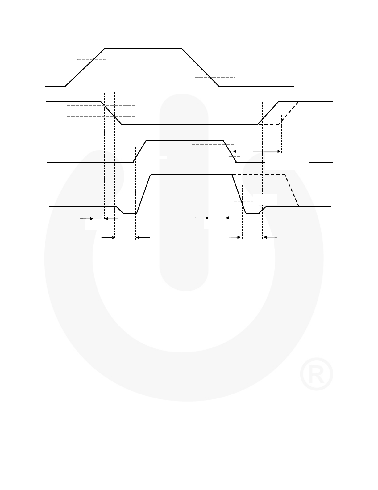
PWM
VSW
V
IH_PWM
FDMF6705V - Extra-Small High-Performance, High-Frequency DrMOS Module
V
IL_PWM
GL
GH
to
VSWH
90%
2.0V
10%
90%
H
t
PD PHGLL
t D_DEADON
10%
t
PD PLGHL
Figure 5. PWM Timing Diagram
1.2V
t
D_DEADOFF
t
D_TIMEOUT
( 250ns Timeout)
2.2V
© 2011 Fairchild Semiconductor Corporation www.fairchildsemi.com
FDMF6705V • Rev. 1.0.2 7
Page 8
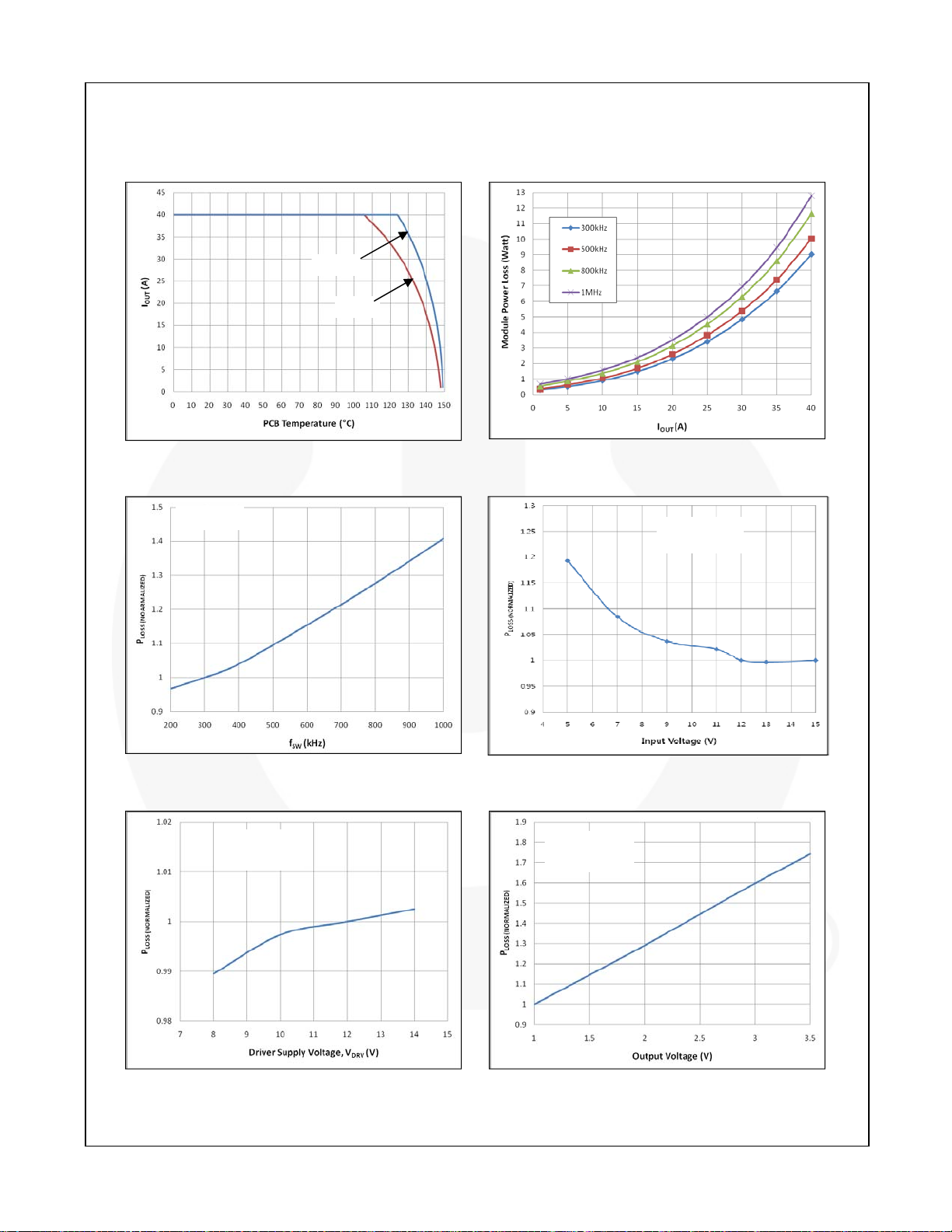
Typical Performance Characteristics
Test Conditions: VIN=12V, V
otherwise specified.
Figure 6. Safe Operating Area Figure 7. Module Power Loss vs. Output Current
=1.0V, V
OUT
300kHz
1MHz
DRV
=12V, L
OUT
FDMF6705V - Extra-Small High-Performance, High-Frequency DrMOS Module
=320nH, TA=25°C, and natural convection cooling, unless
I
=30A
OUT
fSW=300kHz
=30A
I
OUT
Figure 8. Power Loss vs. Switchin g Frequency Figure 9. Power Loss vs. Input Voltage
fSW=300kHz
=30A
I
OUT
fSW=300kHz
I
=30A
OUT
Figure 10. Power Loss vs. Driver Supply Voltage Figure 11. Power Loss vs. Output Voltage
© 2011 Fairchild Semiconductor Corporation www.fairchildsemi.com
FDMF6705V • Rev. 1.0.2 8
Page 9
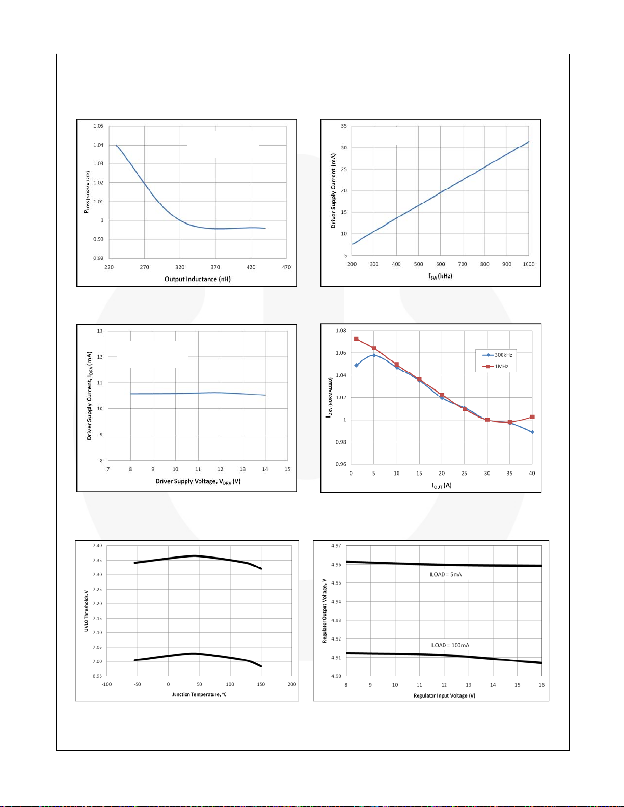
Typical Performance Characteristics (Continued)
Test Conditions: V
=12V, V
IN
otherwise specified.
Figure 12. Power Loss vs. Output Inductance Figure 13. Driver Supply Current vs. Frequency
=1.0V, V
OUT
fSW=300kHz
I
=30A
OUT
DRV
=12V, L
=320nH, TA=25°C, and natural convection cooling, unless
OUT
I
=0A
OUT
FDMF6705V - Extra-Small High-Performance, High-Frequency DrMOS Module
fSW=300kHz
I
=0A
OUT
Figure 14. Driver Supply Current vs. Driver
Supply Voltage
Figure 15. Driver Supply Current vs. Output Current
Figure 16. UVLO Thresholds vs. Temperature Figure 17. LDO Line and Load Regulations
© 2011 Fairchild Semiconductor Corporation www.fairchildsemi.com
FDMF6705V • Rev. 1.0.2 9
Page 10
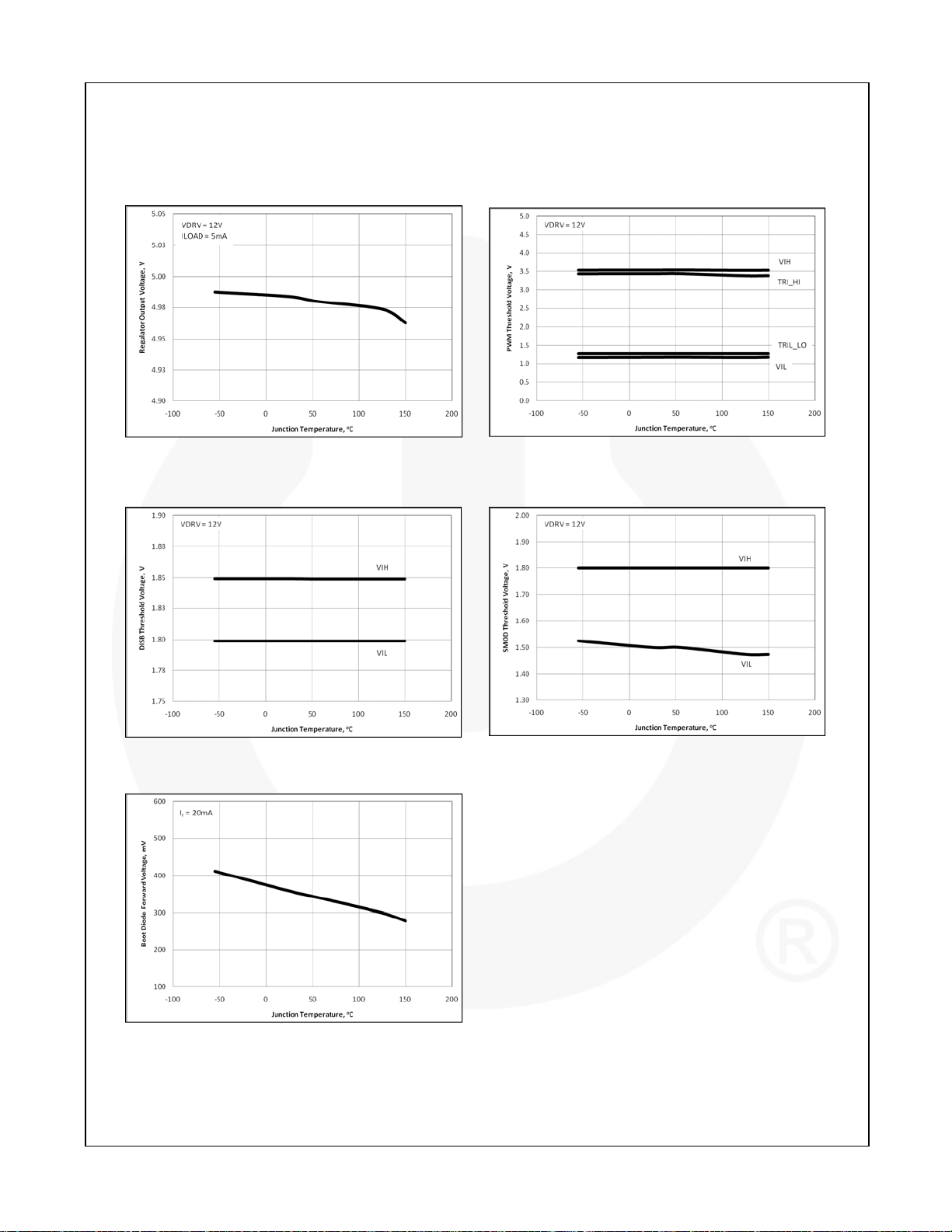
Typical Performance Characteristics (Continued)
Test Conditions: V
=12V, V
IN
otherwise specified.
Figure 18. LDO Output Voltage vs. Temperature Figure 19. PWM Thresholds vs. Temperature
=1.0V, V
OUT
=12V, L
DRV
=320nH, TA=25°C, and natural convection cooling, unless
OUT
FDMF6705V - Extra-Small High-Performance, High-Frequency DrMOS Module
Figure 20. DISB# Thresholds vs. Temperature Figure 21. SMOD# Thresholds vs. Temperature
Figure 22. BOOT Diode VF vs. Temperature
© 2011 Fairchild Semiconductor Corporation www.fairchildsemi.com
FDMF6705V • Rev. 1.0.2 10
Page 11
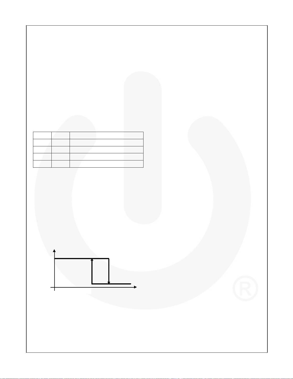
Functional Description
The FDMF6705V is a driver-plus-FET module optimized
for the synchronous buck converter topology. A single
PWM input signal is all that is required to properly drive
the high-side and the low-side MOSFETs. Each part is
capable of driving speeds up to 1MHz.
VDRV and Disable
The VDRV pin is monitored by an under-voltage lockout
(UVLO) circuit. When V
is enabled for operation. When V
the driver is disabled (GH, GL=0). The driver can also
be disabled by pulling the DISB# pin LOW (DISB# <
), which holds both GL and GH LOW regardless
V
IL_DISB
of the PWM input state. The driver can be enabled by
raising the DISB# pin voltage HIGH (DISB# > V
Table 1. UVLO and Disable Logic
UVLO DISB# Driver State
0 X Disabled (GH, GL=0)
1 0 Disabled (GH, GL=0)
1 1 Enabled (See Table 2)
1 Open Disabled (GH, GL=0)
Note:
3. DISB# has an internal pull-down current source of
10µA.
Thermal Warning Flag
The FDMF6705V provides a thermal warning flag
(THWN) to warn of over-temperature conditions. The
thermal warning flag uses an open-drain output that
pulls to CGND when the activation temperature (150°C)
is reached. The THWN output returns to a highimpedance state once the temperature falls to the reset
temperature (135°C). For use, the THWN output
requires a pull-up resistor, which can be connected to
VCIN. THWN does NOT disable the DrMOS module.
High
State
Normal
Operation
THWM Logic
Low
Figure 23. THWN Operation
rises above ~7.3V, the driver
DRV
T
J_drive
135
Reset
Temp.
falls below ~6.95V,
DRV
150°C
°
C
Activation
Temp.
IC
Thermal
Warning
IH_DISB
).
3-State PWM Input
The FDMF6705V incorporates a 3-state PWM input
gate drive design. The 3-state gate drive has both logic
HIGH level and LOW level, along with a 3-state
shutdown window. When the PWM input signal enters
and remains within the 3-state window for a defined
hold-off time (t
D_HOLD-OFF
), both GL and GH are pulled
LOW. This feature enables the gate drive to shut down
both high-and low-side MOSFETs to support features
such as phase shedding, which is a common feature on
multiphase voltage regulators.
Operation when Exiting 3-State Condition
When exiting a valid 3-state condition, the FDMF6705V
design follows the PWM input command. If the PWM
input goes from 3-state to LOW, the low side MOSFET
is turned on. If the PWM input goes from 3-state to
HIGH, the high-side MOSFET is turned on. This is
illustrated in Figure 24. The FDMF6705V design allows
for short propagation delays when exiting the 3-state
window (see Electrical Characteristics).
Low-Side Driver
The low-side driver (GL) is designed to drive a groundreferenced low R
N-channel MOSFET. The bias
DS(ON)
for GL is internally connected between VCIN and
CGND. When the driver is enabled, the driver's output is
180° out of phase with the PWM input. When the driver
is disabled (DISB#=0V), GL is held LOW.
High-Side Driver
The high-side driver is designed to drive a floating Nchannel MOSFET. The bias voltage for the high-side
driver is developed by a bootstrap supply circuit,
consisting of the internal Schottky diode and external
bootstrap capacitor (C
held at PGND, allowing C
through the internal diode. When the PWM input goes
HIGH, GH begins to charge the gate of the high-side
MOSFET (Q1). During this transition, the charge is
removed from C
Q1 turns on, V
V
+ V
IN
BOOT
BOOT
rises to VIN, forcing the BOOT pin to
SWH
, which provides sufficient VGS enhancement
for Q1. To complete the switching cycle, Q1 is turned off
by pulling GH to VSWH. C
VCIN when VSWH falls to PGND. GH output is in-phase
with the PWM input. The high-side gate is held LOW
when the driver is disabled or the PWM signal is held
within the 3-state window for longer than the 3-state
hold-off time, t
D_HOLD-OFF
). During startup, VSWH is
BOOT
to charge to VCIN
BOOT
and delivered to the gate of Q1. As
is then recharged to
BOOT
.
FDMF6705V - Extra-Small High-Performance, High-Frequency DrMOS Module
© 2011 Fairchild Semiconductor Corporation www.fairchildsemi.com
FDMF6705V • Rev. 1.0.2 11
Page 12
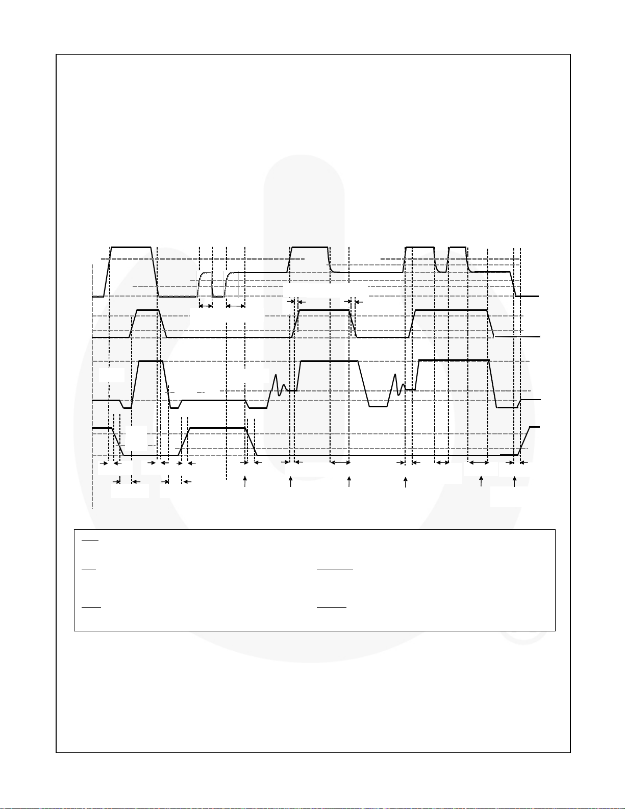
Adaptive Gate Drive Circuit
_
V
The driver IC advanced design ensures minimum
MOSFET dead-time while eliminating potential shoot
through (cross-conduction) currents. It senses the state
of the MOSFETs and adjusts the gate drive adaptively
to ensure they do not conduct simultaneously. Figure 24
provides the relevant timing waveforms. To prevent
overlap during the LOW-to-HIGH switching transition
(Q2 off to Q1 on), the adaptive circuitry monitors the
voltage at the GL pin. When the PWM signal goes
HIGH, Q2 begins to turn off after some propagation
delay (t
PD_PHGLL
~2V, Q1 begins to turn on after adaptive delay t
V
IH_PWM
PWM
). Once the GL pin is discharged below
D_DEADON
V
IH_PWM
V
IL_PWM
t
R_GH
.
To preclude overlap during the HIGH-to-LOW transition
(Q1 off to Q2 on), the adaptive circuitry monitors the
voltage at the VSWH pin. When the PWM signal goes
LOW, Q1 begins to turn off after some propagation
delay (t
PD_PLGHL
Q2 begins to turn on after adaptive delay t
Additionally, V
). Once the VSWH pin falls below ~2.2V,
is monitored. When V
GS(Q1)
D_DEADOFF
GS(Q1)
discharged below ~1.2V, a secondary adaptive delay is
initiated, which results in Q2 being driven on after
t
D_TIMEOUT
implemented to ensure C
, regardless of SW state. This function is
is recharged each
BOOT
switching cycle in the event that the SW voltage does
not fall below the 2.2V adaptive threshold. Secondary
delay t
V
TRI_HI
D_TIMEOUT
t
F_GH
is longer than t
V
IH_PWM
D_DEADOFF
.
V
V
TRI_HI
V
TRI_LO
IL_PWM
V
FDMF6705V - Extra-Small High-Performance, High-Frequency DrMOS Module
.
is
less than
t
OFF
GH
to
VSWH
VSWH
GL
CCM
t
PD_PHGLL
t
90%
2.0V
D_DEADON
t
D_HOLD
2.2
10%
t
PD
PLGHL
t
D_DEADOFF
t
R_GL
D_HOLD -
OFF
-
DCM
t
Enter
3
F_GL
State
-
t
Exit
3-State
PD_TSGHH
t
D_HOLD -OFF
Notes:
t
= propagation delay from external sign al (PWM, SMOD#, etc.) to IC generated signal. Example (t
PD_xxx
t
= delay from IC generated signal to IC generated signal. Example (t
D_xxx
PWM Exiting 3-state
t
= PWM rise to LS VGS fall, V
PD_PHGLL
t
= PWM fall to HS VGS fall, V
PD_PLGHL
= PWM rise to HS VGS rise, V
t
PD_PHGHH
SMOD# Dead Times
t
= SMOD# fall to LS VGS fall, V
PD_SLGLL
= SMOD# rise to LS VGS rise, V
t
PD_SHGLH
to 90% LS VGS t
IH_PWM
to 90% HS VGS t
IL_PWM
to 10% HS VGS (SMOD# held LOW)
IH_PWM
to 90% LS VGS t
IL_SMOD
to 10% LS VGS t
IH_SMOD
– LS VGS (GL) LOW to HS VGS (GH) HIGH)
D_DEADON
PD_TSGHH
PD_TSGLH
D_DEADON
D_DEADOFF
DCM
t
PD_TSGHH
Enter
3
-State
PD_PHGLL
= PWM 3-state to HIGH to HS VGS rise, V
= PWM 3-state to LOW to LS VGS rise, V
= LS VGS fall to HS VGS rise, LS-comp trip value (~2.0V GL) to 10% HS VGS
= VSWH fall to LS VGS rise, SW-comp trip value (~2.2V VSWH) to 10% LS VGS
Exit
3 S t at e
– PWM going HIGH to LS VGS (GL) going LOW)
less than
t
D_HOLD -
IH_PWM
IL_PWM
t
D_HOLD
OFF
Enter
3 -State
to 10% HS VGS
to 10% LS VGS
-
OFF
t
PD_TSGLH
Exit
State
3-
90%
10%
V
V
90%
1
IN
OUT
0%
Figure 24. PWM and 3-StateTiming Diagram
© 2011 Fairchild Semiconductor Corporation www.fairchildsemi.com
FDMF6705V • Rev. 1.0.2 12
Page 13
Skip Mode (SMOD)
V
V
#
The SMOD function allows for higher converter
efficiency under light-load conditions. During SMOD, the
low-side FET gate signal is disabled (held LOW),
preventing discharging of the output capacitors as the
filter inductor current attempts reverse current flow –
also known as “Diode Emulation” Mode.
When the SMOD pin is pulled HIGH, the synchronous
buck converter works in Synchronous Mode, gating on
the low-side FET. When the SMOD pin is pulled LOW,
the low-side FET is gated off. The SMOD pin is
connected to the PWM controller, which enables or
disables the SMOD automatically when the controller
detects light-load condition from output current sensing.
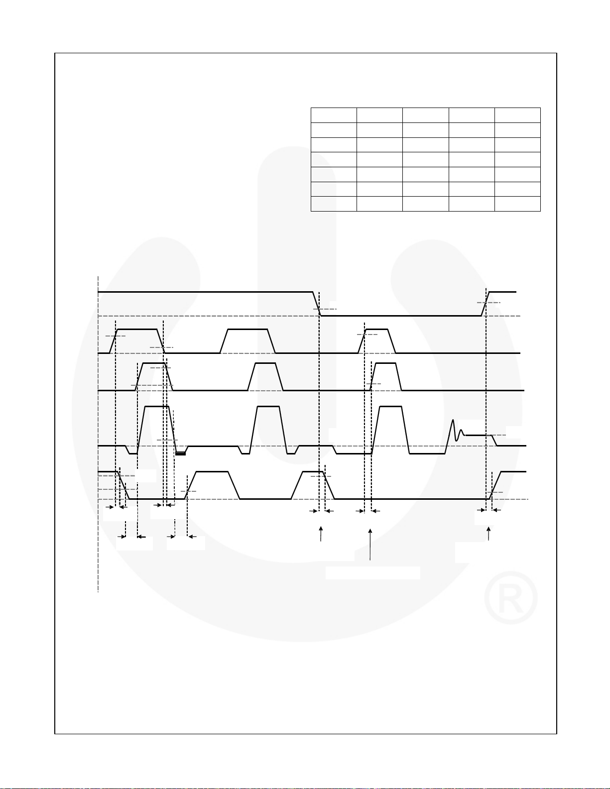
Normally this pin is active LOW. See Figure 25 for
timing delays.
SMOD
V
IH_PWM
V
PWM
GH
to
SWH
IL_PWM
90%
10%
Table 2. SMOD Logic
DISB# PWM SMOD# GH GL
0 X X 0 0
1 3-State X 0 0
1 0 0 0 0
1 1 0 1 0
1 0 1 0 1
1 1 1 1 0
Note:
4. The SMOD feature is intended to have low
propagation delay between the SMOD signal and
the low-side FET VGS response time to control
diode emulation on a cycle-by-cycle basis.
V
V
IL_SMOD
V
IH_PWM
10%
IH_SMOD
FDMF6705V - Extra-Small High-Performance, High-Frequency DrMOS Module
SWH
GL
t
PD_PHGLL
t
D_DEADON
90%
2.0V
t
PD_PLGHL
2.2V
t
D_DEADOFF
10%
CCM
CCM
t
PD_SLGLL
Delay from SMOD# going
LOW to LS VGSLOW
HS turn -on with SMOD# LOW
t
PD_PHGHH
DCM
t
Delay from SMOD# going
HIGH to LS VGSHIGH
PD_SHGLH
10%
V
OUT
Figure 25. SMOD Timing Diagram
© 2011 Fairchild Semiconductor Corporation www.fairchildsemi.com
FDMF6705V • Rev. 1.0.2 13
Page 14
Application Information
A
A
A
Supply Capacitor Selection
For the supply input (VDRV), a local ceramic bypass
capacitor is required to have regulator stable and to
reduce noise. For the regulator output on VCIN, another
local ceramic bypass capacitor is needed to supply the
peak power MOSFET low-side gate current and boot
capacitor charging current. Use at least a 1µF, X7R or
X5R capacitors. Keep these capacitors close to the
FDMF6705V VDRV and VCIN pin and connect them to
GND plane with vias. Do not tie VDRV and VCIN pins
each other.
Bootstrap Circuit
The bootstrap circuit uses a charge storage capacitor
), as shown in Figure 26. A bootstrap capacitance
(C
BOOT
of 100nF X7R or X5R capacitor is adequate. A series
V
DRV
I
DRV
C
VDR
C
VCIN
bootstrap resistor would be needed for specific
applications to improve switching noise immunity.
Power Loss and Efficiency
Measurement and Calculation
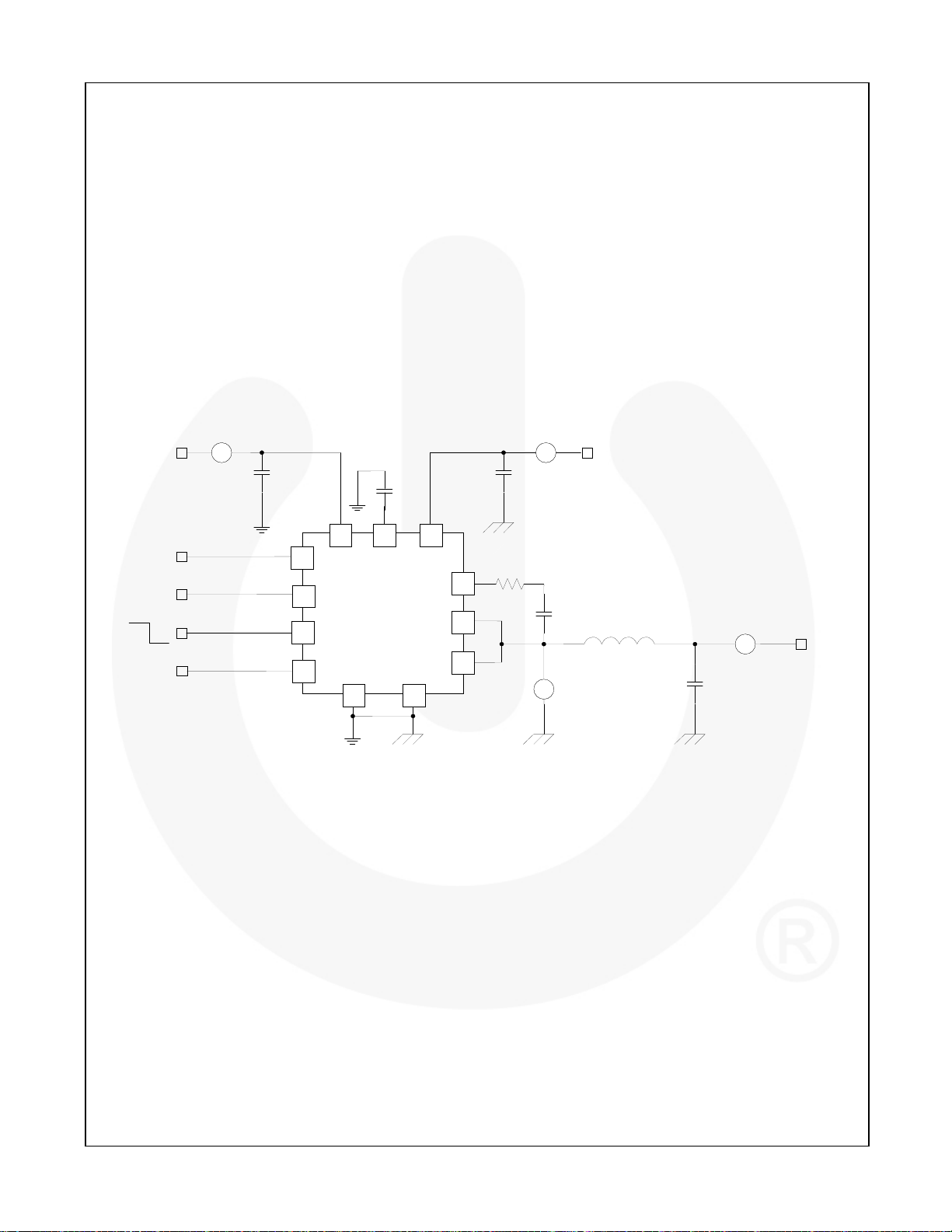
Refer to Figure 26 for power loss testing method. Power
loss calculations are:
=(VIN x IIN) + (V
P
IN
P
SW=VSW
P
OUT=VOUT
P
LOSS_MODULE=PIN
P
LOSS_BOARD=PIN
EFF
MODULE
EFF
BOARD
I
IN
C
VIN
x I
OUT
x I
OUT
=100 x PSW/PIN (%)
=100 x P
DRV
(W)
(W)
- PSW (W)
- P
OUT
OUT/PIN
V
IN
x I
(W)
DRV
(%)
) (W)
FDMF6705V - Extra-Small High-Performance, High-Frequency DrMOS Module
DISB#
PWM Input
OFF
ON
Open-Drain
Output
PGND
VIN
R
BOOT
VSWH
PHASE
BOOT
C
BOOT
L
OUT
V
V
SW
DISB#
PWM
SMOD#
THWN
VCIN
VDRV
FDMF6705V
CGND
Figure 26. Power Loss Measurement Block Diagram
I
OUT
C
OUT
V
OUT
© 2011 Fairchild Semiconductor Corporation www.fairchildsemi.com
FDMF6705V • Rev. 1.0.2 14
Page 15

PCB Layout Guidelines
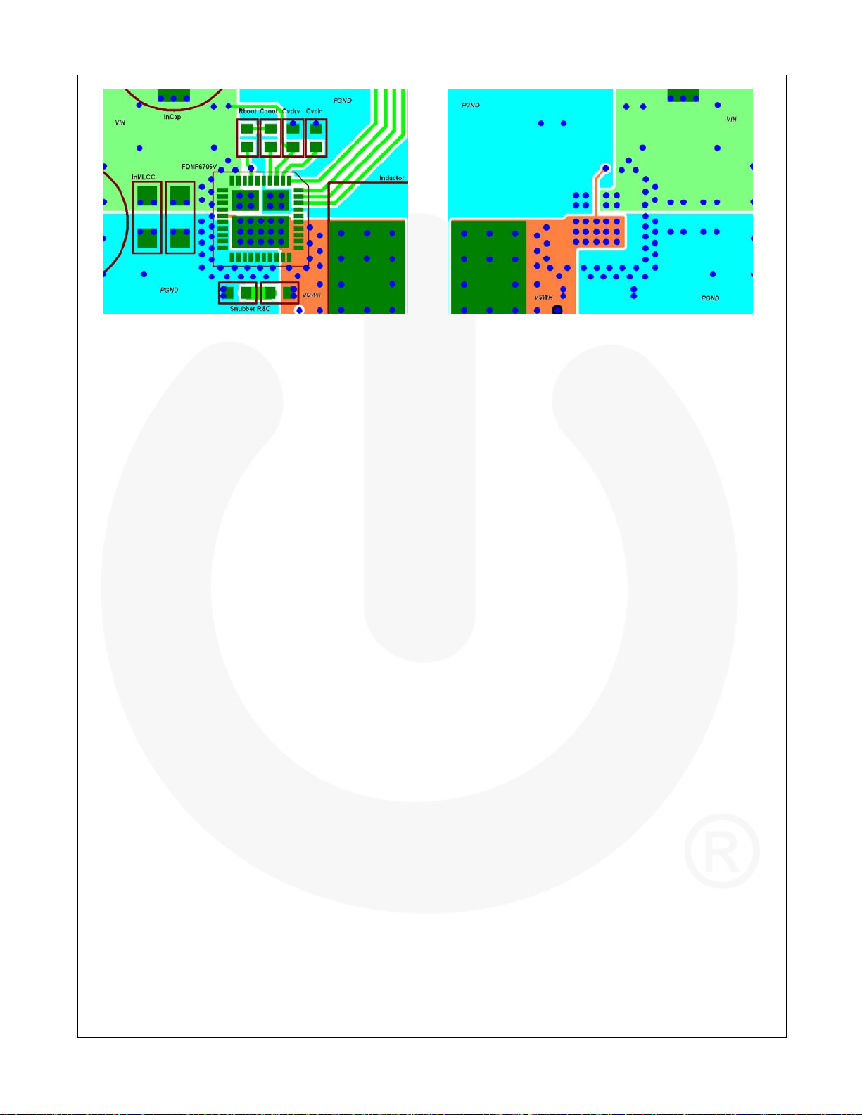
Figure 27 provides an example of a proper layout for the
FDMF6705V and critical components. All of the highcurrent paths, such as V
IN
, V
SWH
, V
OUT
, and GND
copper, should be short and wide for low inductance
and resistance. This technique aids in achieving a more
stable and evenly distributed current flow, along with
enhanced heat radiation and system performance.
The following guidelines are recommendations for the
PCB designer:
1. Input ceramic bypass capacitors must be placed
close to the VIN and PGND pins. This helps
reduce the high-current power loop inductance
and the input current ripple induced by the power
MOSFET switching operation.
2. The V
copper trace serves two purposes. In
SWH
addition to being the high-frequency current path
from the DrMOS package to the output inductor, it
also serves as a heat sink for the low-side
MOSFET in the DrMOS package. The trace
should be short and wide enough to present a lowimpedance path for the high-frequency, highcurrent flow between the DrMOS and inductor to
minimize losses and temperature rise. Note that
the VSWH node is a high voltage and highfrequency switching node with high noise
potential. Care should be taken to minimize
coupling to adjacent traces. Since this copper
trace also acts as a heat sink for the lower FET,
balance using the largest area possible to improve
DrMOS cooling while maintaining acceptable
noise emission.
3. An output inductor should be located close to the
FDMF6705V to minimize the power loss due to the
VSWH copper trace. Care should also be taken so
the inductor dissipation does not heat the DrMOS.
4. PowerTrench® MOSFETs are used in the output
stage. The Power MOSFETs are effective at
minimizing ringing due to fast switching. In most
cases, no VSWH snubber is required. If a snubber
is used, it should be placed close to the VSWH and
PGND pins. The resistor and capacitor need to be
of proper size for the power dissipation.
5. VCIN, VDRV, and BOOT capacitors should be
placed as close as possible to the VCIN to CGND,
VDRV to CGND, and BOOT to PHASE pins to
ensure clean and stable power. Routing width and
length should be considered as well.
6. Include a trace from PHASE to VSWH to improve
noise margin. Keep the trace as short as possible.
© 2011 Fairchild Semiconductor Corporation www.fairchildsemi.com
FDMF6705V • Rev. 1.0.2 15
7. The layout should include the option to insert a
small-value series boot resistor between the boot
capacitor and BOOT pin. The boot-loop size,
including R
BOOT
and C
, should be as small as
BOOT
possible. The boot resistor is normally not
required, but is effective at controlling the highside MOSFET turn-on slew rate. This can improve
noise operating margin in synchronous buck
designs that may have noise issues due to ground
bounce or high positive and negative VSWH
ringing. Inserting a boot resistance lowers the
DrMOS efficiency. Efficiency versus noise tradeoffs must be considered.
The VIN and PGND pins handle large current
transients with frequency components greater than
100MHz. If possible, these pins should be
connected directly to the VIN and board GND
planes. The use of thermal relief traces in series
with these pins is discouraged since this adds
inductance to the power path. This added
inductance in series with either the VIN or PGND
pin degrades system noise immunity by increasing
positive and negative VSWH ringing.
8. CGND pad and PGND pins should be connected
by plane GND copper with multiple vias for stable
grounding. Poor grounding can create a noise
transient offset voltage level between CGND and
PGND. This could lead to faulty operation of gate
driver and MOSFET.
9. Ringing at the BOOT pin is most effectively
controlled by close placement of the boot
capacitor. Do not add an additional BOOT to the
PGND capacitor. This may lead to excess current
flow through the BOOT diode.
10. The SMOD# and DISB# pins have weak internal
pull-up and pull-down current sources,
respectively. These pins should not have any
noise filter capacitors. Do not to float these pins
unless absolutely necessary.
11. Use multiple vias on each copper area to
interconnect top, inner, and bottom layers to help
distribute current flow and heat conduction. Vias
should be relatively large and of reasonably low
inductance. Critical high-frequency components,
such as R
BOOT
, C
, the RC snubber, and
BOOT
bypass capacitors should be located as close to
the respective DrMOS module pins as possible
on the top layer of the PCB. If this is not feasible,
they should be connected from the backside
through a network of low-inductance vias.
FDMF6705V - Extra-Small High-Performance, High-Frequency DrMOS Module
Page 16
FDMF6705V - Extra-Small High-Performance, High-Frequency DrMOS Module
Bottom View Top View
Figure 27. PCB Layout Example
© 2011 Fairchild Semiconductor Corporation www.fairchildsemi.com
FDMF6705V • Rev. 1.0.2 16
Page 17
Physical Dimensions
B
0.10
2X
0.50
0.40
2.00±0.10
0.10
0.08
0.40
(0.70)
C
C
11
20
C
1.10
0.90
6.00
TOP VIEW
FRONT VIEW
4.40±0.10
(2.20)
21
10
(0.20)
BOTTOM VIEW
0.30
0.20
DETAIL 'A'
(0.20)
0.05
0.00
SCALE: 2:1
0.30
0.20
30
31
2.40±0.10
1.50±0.10
40
1
2.00±0.10
0.50
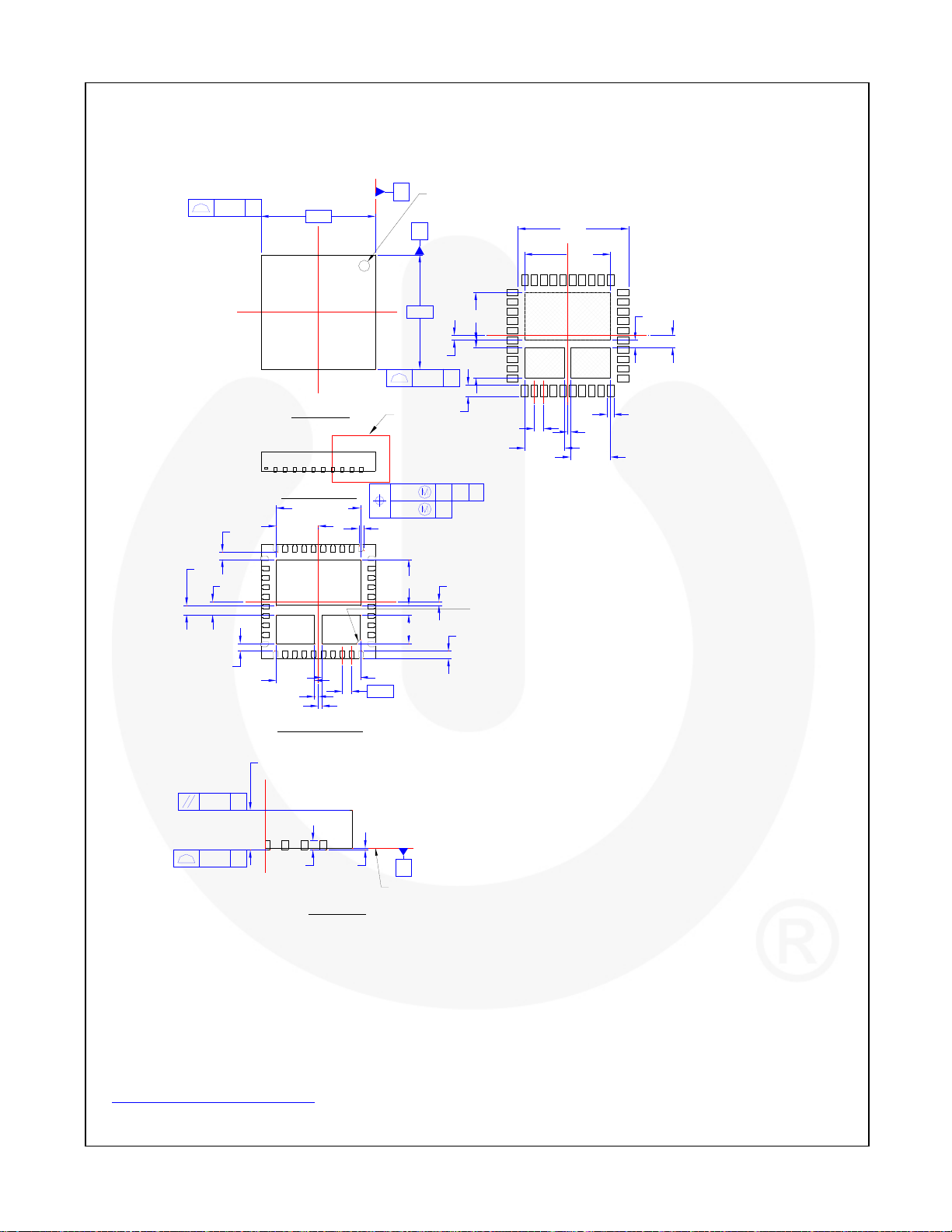
Figure 28. 40-Lead, Clipbond PQFN DrMOS, 6.0x6.0mm Package
Package drawings are provided as a service to customers considering Fairchild components. Drawings may change in any manner
without notice. Please note the revision and/or date on the drawing and contact a Fairchild Semiconductor representative to verify or
obtain the most recent revision. Package specifications do not expand the terms of Fairchild’s worldwide terms and conditions, specifically the
warranty therein, which covers Fairchild products.
Always visit Fairchild Semiconductor’s online packaging area for the most recent package drawings:
http://www.fairchildsemi.com/packaging/
.
PIN#1
INDICATOR
A
6.00
0.25
0.10 C
2X
0.60
SEE
DETAIL 'A'
0.10 CAB
C
0.05
(40X)
0.20
0.50
0.30
NOTES: UNLESS OTHERWISE SPECIFIED
A) DOES NOT FULLY CONFORM TO JEDEC
B) ALL DIMENSIONS ARE IN MILLIMETERS.
C) DIMENSIONS DO NOT INCLUDE BURRS
OR MOLD FLASH. MOLD FLASH OR
BURRS DOES NOT EXCEED 0.10MM.
D) DIMENSIONING AND TOLERANCING PER
ASME Y14.5M-1994.
E) DRAWING FILE NAME: PQFN40AREV2
C
SEATING
PLANE
5.80
4.50
31
2.50
1.60
40
1
0.50 TYP
2.10
LAND PATTERN
RECOMMENDATION
PIN #1 INDICATOR
(40X)
REGISTRATION MO-220, DATED
MAY/2005.
2130
10
0.15
2.10
20
0.40
0.65
11
0.35
FDMF6705V - Extra-Small High-Performance, High-Frequency DrMOS Module
© 2011 Fairchild Semiconductor Corporation www.fairchildsemi.com
FDMF6705V • Rev. 1.0.2 17
Page 18
FDMF6705V - Extra-Small High-Performance, High-Frequency DrMOS Module
© 2011 Fairchild Semiconductor Corporation www.fairchildsemi.com
FDMF6705V • Rev. 1.0.2 18
 Loading...