

Page 1
tm
August 2009
FDMF6704A - XSTM DrMOS
The Xtra Small, High Performance, High Frequency DrMOS Module
FDMF6704A
The Xtra Small, High Performance, High Frequency DrMOS Module
Benefits
Ultra compact size - 6 mm x 6 mm MLP, 44 % space
saving compared to conventional MLP 8 mm x 8 mm
DrMOS packages.
Fully optimized system efficiency.
Clean voltage waveforms with reduced ringing.
High frequency operation.
Features
Ultra- compact thermally enhanced 6 mm x 6 mm MLP
package 84 % smaller than conventional discrete solutions.
Synchronous driver plus FET multichip module.
High current handling of 35 A.
Over 93 % peak efficiency.
Logic level PWM input.
Fairchild's PowerTrench® 5 technology MOSFETs for clean
voltage waveforms and reduced ringing.
Optimized for high switching frequencies of up to 1 MHz.
Skip mode SMOD [low side gate turn off] input.
Fairchild SyncFETTM [integrated Schottky diode] technology
in the low side MOSFET.
Integrated bootstrap Schottky diode.
Adaptive gate drive timing for shoot-through protection.
Driver output disable function [DISB# pin].
Undervoltage lockout (UVLO).
Fairchild Green Packaging and RoHS
compliant. Low profile SMD package.
General Description
The XSTM DrMOS family is Fairchild’s next-generation fullyoptimized, ultra-compact, integrated MOSFET plus driver power
stage solutions for high current, high frequency synchronous
buck DC-DC applications. The FDMF6704A XSTM DrMOS
integrates a driver IC, two power MOSFETs and a bootstrap
Schottky diode into a thermally enhanced, ultra compact 6 mm x
6 mm MLP package. With an integrated approach, the complete
switching power stage is optimized with regards to driver and
MOSFET dynamic performance, system inductance and
R
. This greatly reduces the package parasitics and layout
DS(ON)
challenges associated with conventional discrete solutions.
XSTM DrMOS uses Fairchild's high performance
PowerTrenchTM 5 MOSFET technology, which dramatically
reduces ringing in synchronous buck converter applications.
PowerTrenchTM 5 can eliminate the need for a snubber circuit in
buck converter applications. The driver IC incorporates
advanced features such as SMOD for improved light load
efficiency. A 5 V gate drive and an improved PCB interface
optimized for a maximum low side FET exposed pad area,
ensure higher performance. This product is compatible with
the new Intel 6 mm x 6 mm DrMOS specification.
Applications
Compact blade servers V-core, non V-core and VTT DC-DC
converters.
Desktop computers V-core, non V-core and VTT DC-DC
converters.
Workstations V-core, non V-core and VTT DC-DC
converters.
Gaming Motherboards V-core, non V-core and VTT DC-DC
converters.
Gaming consoles.
High-current DC-DC Point of Load (POL) converters.
Networking and telecom microprocessor voltage regulators.
Small form factor voltage regulator modules.
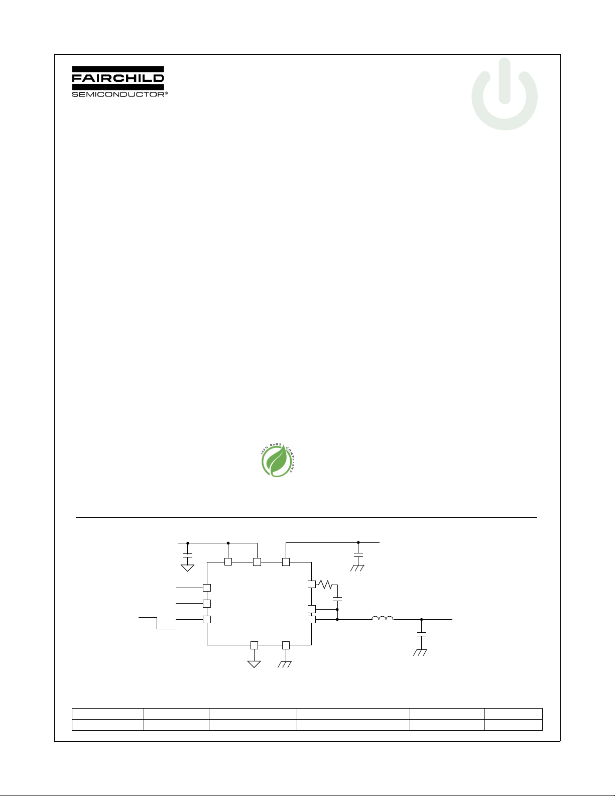
Power Train Application Circuit
5 V
C
VDRV
DISB#
PWM Input
OFF
ON
VCIN VIN
VDRV
DISB#
PWM
SMOD#
BOOT
PHASE
VSWH
CGND PGND
R
BOOT
C
BOOT
Figure 1. Power Train Application Circuit
12 V
C
VIN
L
OUT
OUTPUT
C
OUT
Ordering Information
Order Number Marking Temperature Range Device Package Packing Method Quantity
FDMF6704A FDMF6704A_1 -55 °C to 150 °C 40 Pin, 3 DAP, MLP 6x6 mm Tape and Reel 3000
©2008 Fairchild Semiconductor Corporation
FDMF6704A Rev. F
1
www.fairchildsemi.com
Page 2
Functional Block Diagram
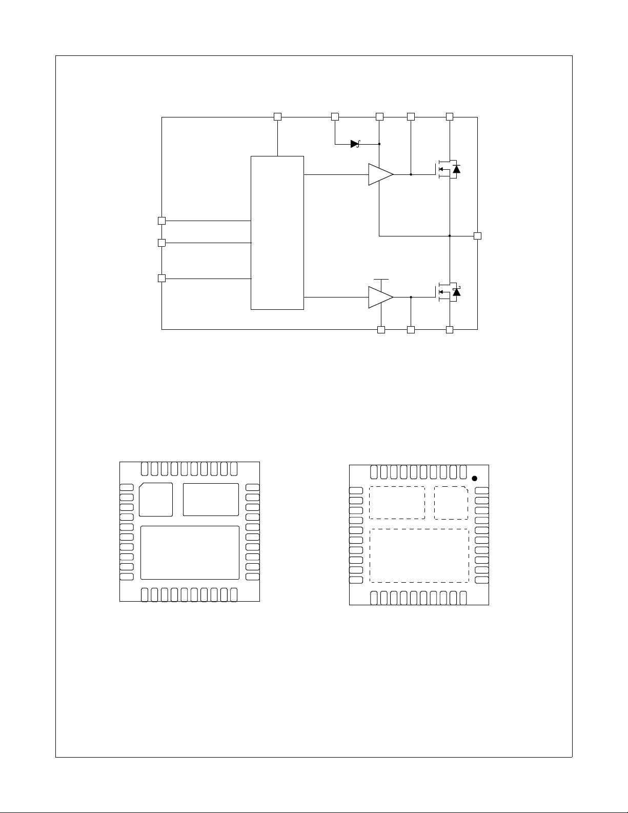
Figure 2. Functional Block Diagram
CGND
PGND
VSWH
VIN
BOOT
VCIN
VDRV
GH
GL
VDRV
PWM
DISB#
Overlap
Control
SMOD#
Q2
Q1
Figure 3. 6mm x 6mm, 40L MLP
CGND
V
IN
VSWH
CGND
V
IN
VSWH
PWM
SMOD#
DISB#
NC
CGND
GL
VSWH
VSWH
VSWH
VSWH
VSWH
VCIN
VDRV
BOOT
CGND
GH
NC
VIN
VIN
VIN
VIN
VIN
VIN
VSWH
PGND
VSWH
VSWH
PGND
PGND
PGND
PGND
PGND
PGND
PGND
PHASE
PGND
PGND
PGND
PGND
PGND
Bottom View Top View
1
2
3
4
5
6
7
8
9
10
11
12
13
14
15
16
17
18
19
20
30
29
28
27
26
25
24
23
22
21
40
39
38
37
36
35
34
33
32
31
123456789
10
40
39
38
37
36
35
34
33
32
31
302928272625242322
21
11
12
13
14
15
16
17
18
19
20
SMOD#
VCIN
VDRV
BOOT
CGND
GH
NC
VIN
VIN
PHASE
VIN
VIN
VIN
VIN
VSWH
PGND
PGND
PGND
PGND
PGND
PGND
VSWH
VSWH
PGND
PGND
PGND
PGND
PGND
PGND
PGND
PWM
DISB#
NC
CGND
GL
VSWH
VSWH
VSWH
VSWH
VSWH
41
42
43
41
42
43
FDMF6704A
The Xtra Small, High Performance, High Frequency DrMOS Module
Pin Configuration
FDMF6704A Rev. F
2
www.fairchildsemi.com
Page 3
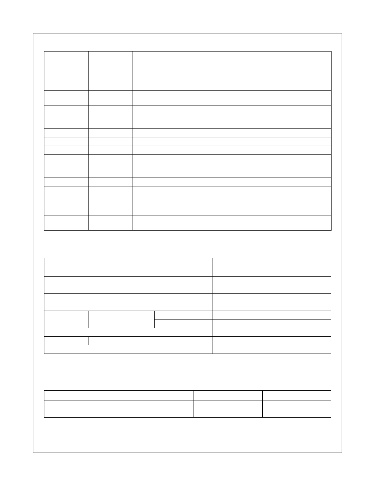
Pin Description
Pin Name Function
1 SMOD#
2 VCIN IC bias supply. Minimum 1 F ceramic capacitor is recommended from this pin to CGND.
3 VDRV
4 BOOT
5, 37, 41 CGND IC ground. Ground return for driver IC.
6 GH For manufacturing test only. This pin must be floated. Must not be connected to any pin.
7 PHASE Switch node pin for easy bootstrap capacitor routing. Electrically shorted to VSWH pin.
8, 38 NC No connect.
9-14, 42 VIN Power input. Output stage supply voltage.
15, 29-35, 43 VSWH, PHASE
16-28 PGND Power ground. Output stage ground. Source pin of low side MOSFET(s).
36 GL For manufacturing test only. This pin must be floated. Must not be connected to any pin.
39 DISB#
40 PWM
When SMOD# = HI, low side driver is inverse of PWM input. When SMOD# = Low, low
side driver is disabled. This pin has no internal pullup or pulldown. It should not be left
floating. Do not add noise filter cap.
Power for low side driver. Minimum 1 F ceramic capacitor is recommended to be
connected as close as possible from this pin to CGND.
Bootstrap supply input. Provides voltage supply to high-side MOSFET driver. Connect
bootstrap capacitor from this pin to PHASE.
Switch node input. Provides return for high-side bootstrapped driver and acts as a
sense point for the adaptive shoot-thru protection.
Output disable. When low, this pin disable FET switching (GH and GL are held low). This
pin has no internal pullup or pulldown. It should not be left floating. Do not add noise filter
cap.
PWM Signal Input. This pin accepts a logic-level PWM signal from the controller. This pin
has no internal pullup or pulldown. It should not be left floating. Do not add noise filter cap.
FDMF6704A
The Xtra Small, High Performance, High Frequency DrMOS Module
Absolute Maximum Rating
Parameter Min Max Units
VCIN, VDRV, DISB#, PWM, SMOD#, GL to CGND 6 V
VIN to PGND, CGND 27 V
BOOT, GH to VSWH, PHASE 6 V
BOOT, VSWH, PHASE, GH to GND 27 V
BOOT to VDRV 22 V
I
* V
O(AV)
I
* 80 A
O(peak)
R
θJPCB
Operating and Storage Junction Temperature Range -55 150 °C
* I
and I
O(AV)
O(peak)
= 12 V, VO = 1.3 V
IN
Junction to PCB Thermal Resistance 3.75 °C/W
are measured in FCS evaluation board. These ratings can be changed with different application setting.
fSW = 350 kHz 35 A
fSW = 1 MHz 32 A
Recommended Operating Range
Parameter Min Typ Max Units
V
CIN
V
IN
* May be operated at lower input voltage. See figure 10.
Control Circuit Supply Voltage 4.5 5 5.5 V
Output Stage Supply Voltage 3
*
12 14 V
FDMF6704A Rev. F
3
www.fairchildsemi.com
Page 4
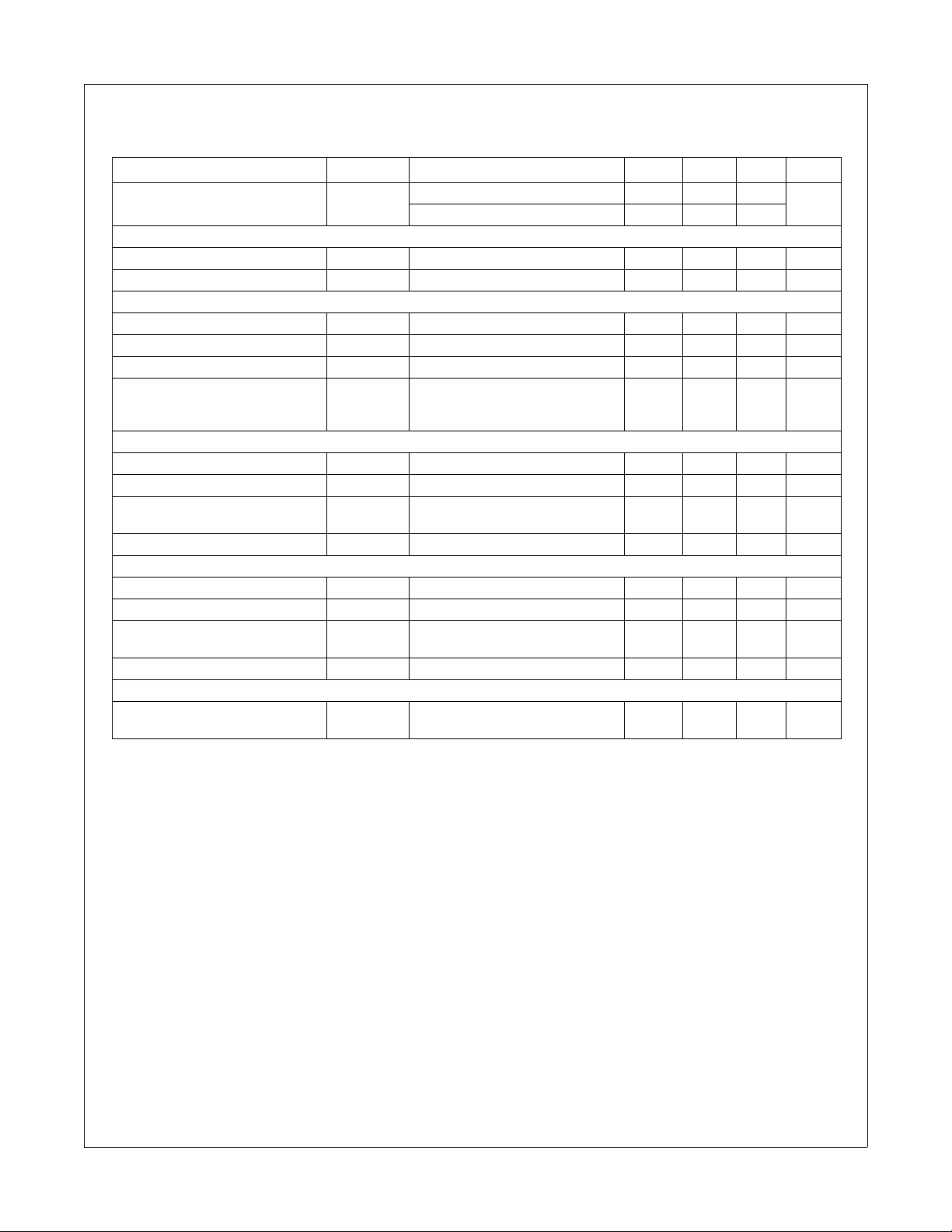
Electrical Characteristics
VIN = 12 V, TA = 25 °C unless otherwise noted.
Parameter Symbol Conditions Min Typ Max Units
Operating Quiescent Current IQ
VCIN UVLO
UVLO Threshold 3.0 3.2 3.4 V
UVLO COMP Hysteresis 0.2 V
PWM, DISB# and SMOD# Input
High Level Input Voltage 2 V
Low Level Input Voltage 0.8 V
Input Bias Current -2 2 A
Propagation Delay Time
High Side Driver
Rise Time 10 % to 90 % 25 ns
Fall Time 90 % to 10 % 20 ns
Deadband Time t
Propagation Delay t
Low Side Driver
Rise Time 10 % to 90 % 25 ns
Fall Time 90 % to 10 % 20 ns
Deadband Time t
Propagation Delay t
250 ns Time Out Circuit
250 ns Time Delay
DTHH
PDHL
DTLH
PDLL
PWM = GND 2
PWM = V
PWM = GND, delay between SMOD#
or DISB# from HI to LO to GL from HI
to LO.
GL going LO to GH going HI, 10 % to
10 %
PMW going LO to GH going LO 10 ns
VSWH going LO to GL going HI, 10
% to 10 %
PWM going HI to GL going LO 10 ns
Delay between GH from HI to LO and
GL from LO to HI.
CIN
15 ns
25 ns
20 ns
250 ns
2
mA
FDMF6704A
The Xtra Small, High Performance, High Frequency DrMOS Module
FDMF6704A Rev. F
4
www.fairchildsemi.com
Page 5

FDMF6704A
Description of Operation
Circuit Description
The FDMF6704A is a driver plus FET module optimized for
synchronous buck converter topology. A single PWM input
signal is all that is required to properly drive the high-side and
the low-side MOSFETs. Each part is capable of driving speeds
up to 1 MHz.
Low-Side Driver
The low-side driver (GL) is designed to drive a ground
referenced low R
internally connected between VDRV and CGND. When the
driver is enabled, the driver's output is 180° out of phase with
the PWM input. When the driver is disabled (DISB = 0 V), GL is
held low.
High-Side Driver
The high-side driver (GH) is designed to drive a floating
N-channel MOSFET. The bias voltage for the high-side driver is
developed by a bootstrap supply circuit, consisting of the
internal diode and external bootstrap capacitor (C
start-up, VSWH is held at PGND, allowing C
V
through the internal diode. When the PWM input goes
DRV
high, GH will begin to charge the high-side MOSFET's gate
(Q1). During this transition, charge is removed from C
delivered to Q1's gate. As Q1 turns on, VSWH rises to VIN,
forcing the BOOT pin to VIN +V
sufficient VGS enhancement for Q1. To complete the switching
cycle, Q1 is turned off by pulling GH to VSWH. C
recharged to VDRV when VSWH falls to PGND. GH output is in
phase with the PWM input. When the driver is disabled, the
high-side gate is held low.
N-channel MOSFET. The bias for GL is
DS(ON)
BOOT
, which provides
C(BOOT)
). During
BOOT
to charge to
and
BOOT
is then
BOOT
Adaptive Gate Drive Circuit
The driver IC embodies an advanced design that ensures
minimum MOSFET dead-time while eliminating potential
shoot-through (cross-conduction) currents. It senses the state of
the MOSFETs and adjusts the gate drive, adaptively, to ensure
they do not conduct simultaneously. Refer to Figure 4 for the
relevant timing waveforms.
To prevent overlap during the low-to-high switching transition
(Q2 OFF to Q1 ON), the adaptive circuitry monitors the voltage
at the GL pin. When the PWM signal goes HIGH, Q2 will begin
to turn OFF after some propagation delay (t
pin is discharged below 1 V, Q1 begins to turn ON after adaptive
delay t
To preclude overlap during the high-to-low transition (Q1 OFF to
Q2 ON), the adaptive circuitry monitors the voltage at the
VSWH pin. When the PWM signal goes LOW, Q1 will begin to
turn OFF after some propagation delay (t
VSWH pin falls below 1 V, Q2 begins to turn ON after adaptive
delay t
Additionally, VGS of Q1 is monitored. When V
discharged low, a secondary adaptive delay is initiated, which
results in Q2 being driven ON after 250 ns, regardless of VSWH
state. This function is implemented to ensure C
recharged each switching cycle, particularly for cases where the
power convertor is sinking current and VSWH voltage does not
fall below the 1 V adaptive threshold. The 250 ns secondary
delay is longer than t
DTHH
DTLH
.
.
.
DTLH
). Once the GL
PDLL
). Once the
PDHL
GS(Q1)
BOOT
is
is
The Xtra Small, High Performance, High Frequency DrMOS Module
SMOD
The SMOD (Skip Mode) function allows for higher converter
efficiency under light load conditions. During SMOD, the LS
FET is disabled and it prevents discharging of output caps.
When the SMOD# pin is pulled high, the sync buck converter
will work in synchronous mode. When the SMOD# pin is pulled
low, the LS FET is turned off. The SMOD function does not have
internal current sensing. This SMOD# pin is connected to a
PWM controller which enables or disables the SMOD
automatically when the controller detects light load condition.
Normally this pin is Active Low.
FDMF6704A Rev. F
5
www.fairchildsemi.com
Page 6
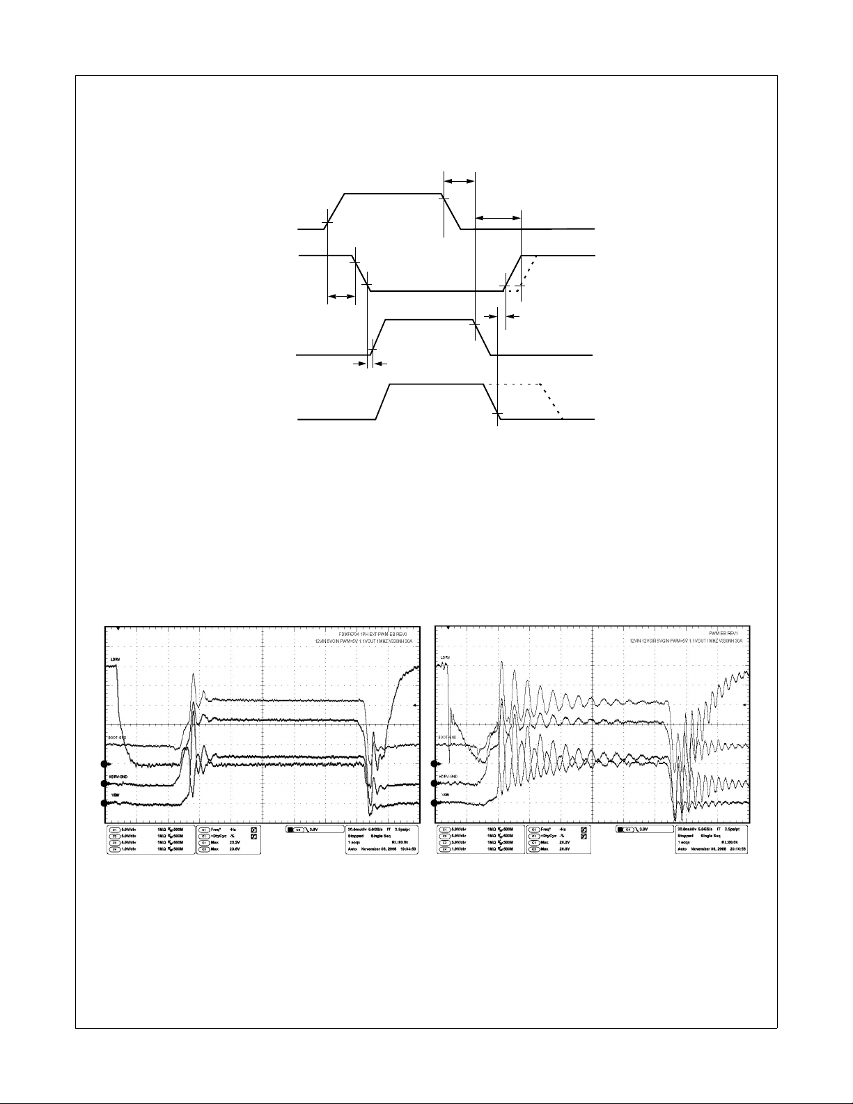
Timing Diagrams
Figure 4. Timing Diagram
PWM
t
PDLL
GH to VSWH
t
DTLH
GL
VSWH
t
PDHL
Timeout
t
DTHH
FDMF6704A
The Xtra Small, High Performance, High Frequency DrMOS Module
Switch Node Ringing Suppression
Fairchild's DrMOS products have proprietary feature* that minimizes the peak overshoot and ringing voltage on the switch node
(VSWH) output, without the need of external snubbers. The following pictures show the waveforms of an FDMF6704 DrMOS part and
a competitor's part tested without snubbing. The tests were done in the same test circuit, under the same operating conditions.
Figure 5. FDMF6704 Figure 6. Competitor Part
* Patent Pending
FDMF6704A Rev. F
6
www.fairchildsemi.com
Page 7
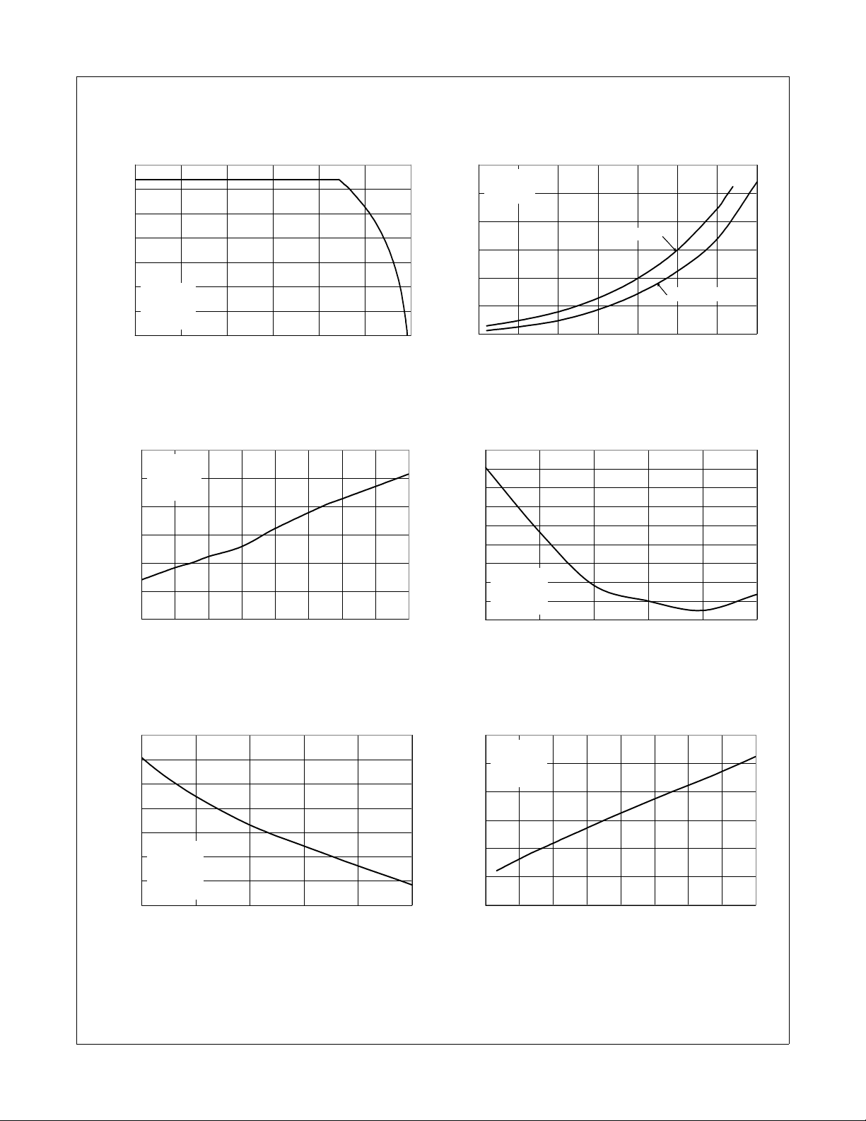
Typical Characteristics
0
5
10
15
20
25
30
35
0 25 50 75 100 125 150
PCB Temperature, oC
I
LOAD
, A
VIN = 12 V
V
OUT
= 1.3 V
fSW = 1 MHz
L = 440 nH
0
2
4
6
8
10
12
0 5 10 15 20 25 30 35
I
LOAD
, A
P
LOSS
, W
fSW = 1 MHz
fSW = 350 kHz
VIN = 12 V
V
OUT
= 1.3 V
L = 440 nH
0.98
1.00
1.02
1.04
1.06
1.08
1.10
1.12
1.14
1.16
6 8 10 12 14 16
Input Voltage, V
P
LOSS (NORMALIZED)
V
OUT
= 1.3 V
I
OUT
= 30 A
L = 440 nH
fSW = 350 kHz
0.80
0.90
1.00
1.10
1.20
1.30
1.40
0.8 1.1 1.4 1.7 2.0 2.3 2.6 2.9 3.2
Output Voltage, V
P
LOSS (NORMALIZED)
VIN = 12 V
I
OUT
= 30 A
L = 440 nH
fSW = 350 kHz
0.80
0.90
1.00
1.10
1.20
1.30
1.40
200 300 400 500 600 700 800 900 1000
fSW, kHz
P
LOSS (NORMALIZED)
VIN = 12 V
V
OUT
= 1.3 V
I
OUT
= 30 A
L = 440 nH
0.89
0.92
0.95
0.98
1.01
1.04
1.07
1.10
4.5 4.8 5.1 5.4 5.7 6.0
Driver Supply Voltage, V
P
LOSS (NORMALIZED)
VIN = 12 V
V
OUT
= 1.3 V
I
OUT
= 30 A
L = 440 nH
fSW = 350 kHz
VIN = 12V, V
= 5V, TA = 25°C unless otherwise noted.
CIN
Figure 7. Safe Operating Area Figure 8. Module Power Loss vs. Output Current
FDMF6704A
The Xtra Small, High Performance, High Frequency DrMOS Module
Figure 9. Power Loss vs. Switching Frequency Figure 10. Power Loss vs. Input Voltage
FDMF6704A Rev. F
Figure 11. Power Loss vs. Driver Supply Voltage Figure 12. Power Loss vs. Output Voltage
7
www.fairchildsemi.com
Page 8
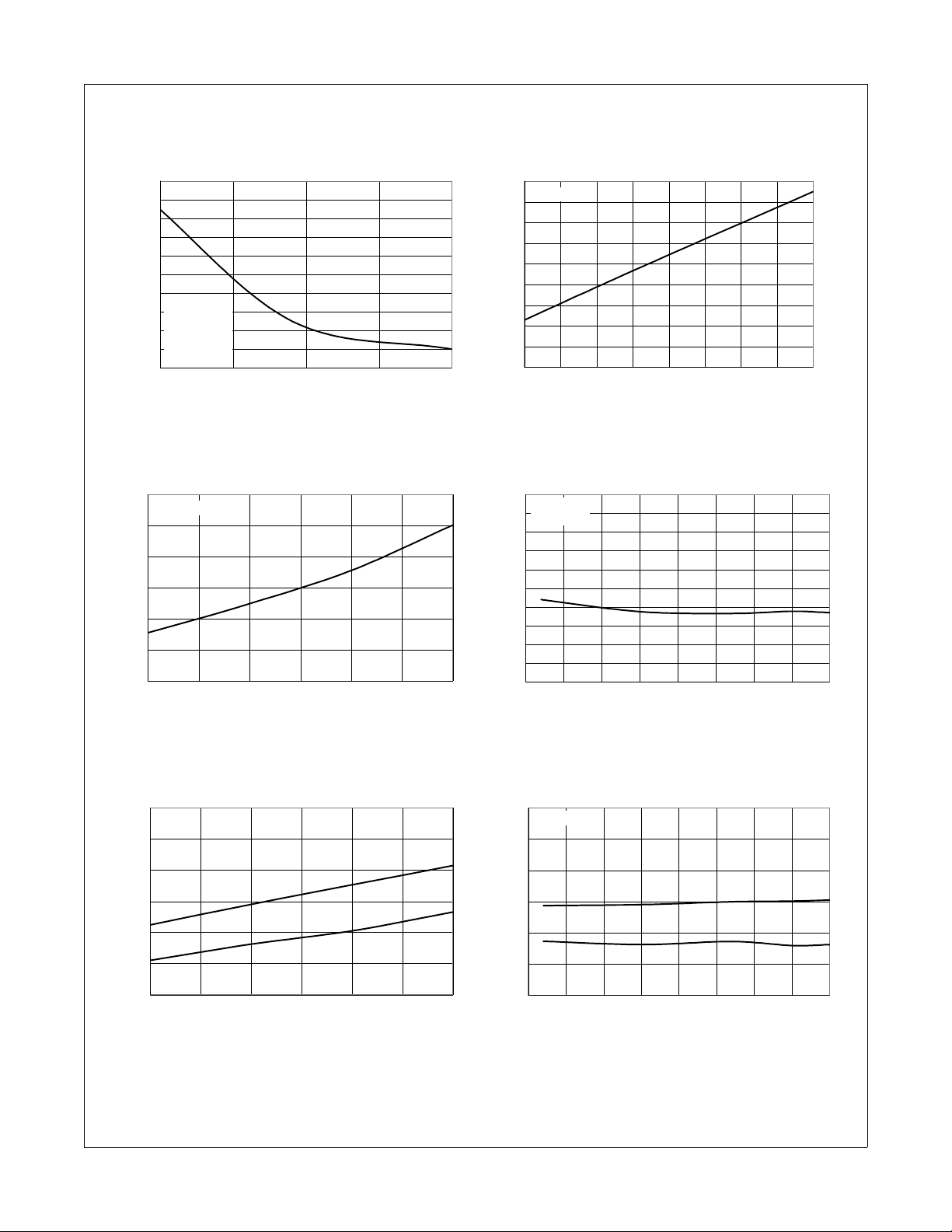
Typical Characteristics
0.995
1.000
1.005
1.010
1.015
1.020
1.025
1.030
1.035
1.040
1.045
220 275 330 385 440
Output Inductance, nH
P
LOSS (NORMALIZED)
VIN = 12 V
V
OUT
= 1.3 V
I
OUT
= 30 A
fSW = 350 kHz
0
5
10
15
20
25
30
35
40
45
200 300 400 500 600 700 800 900 1000
fSW, kHz
Driver Supply Current, mA
V
CIN
= 5 V
30
35
40
45
50
55
60
4.5 4.8 5.0 5.3 5.5 5.8 6.0
Driver Supply Voltage, V
Driver Supply Current, mA
fSW = 1 MHz
40
41
42
43
44
45
46
47
48
49
50
-50 -25 0 25 50 75 100 125 150
Temperature, oC
Driver Supply Current, mA
V
CIN
= 5 V
fSW = 1 MHz
1.0
1.2
1.4
1.6
1.8
2.0
2.2
4.5 4.8 5.0 5.3 5.5 5.8 6.0
Driver Supply Voltage, V
PWM Threshold Voltage, V
V
IH
V
IL
1.0
1.2
1.4
1.6
1.8
2.0
2.2
-50 -25 0 25 50 75 100 125 150
Temperature, oC
PWM Threshold Voltage, V
V
IH
V
IL
V
CIN
= 5 V
1.0
1.2
1.4
1.6
1.8
2.0
2.2
4.5 4.8 5.0 5.3 5.5 5.8 6.0
Driver Supply Voltage, V
PWM Threshold Voltage, V
V
IH
V
IL
VIN = 12V, V
= 5V, TA = 25°C unless otherwise noted.
CIN
Figure 13. Power Loss vs. Output Inductance Figure 14. Driver Supply Current vs. Frequency
FDMF6704A
The Xtra Small, High Performance, High Frequency DrMOS Module
Figure 15. Driver Supply Current vs. Drive Supply Voltage
Figure 17. PWM Threshold Voltage vs. Driver Supply Voltage
FDMF6704A Rev. F
Figure 16. Driver Supply Current vs. Temperature
Figure 18. PWM Threshold Voltage vs. Temperature
8
www.fairchildsemi.com
Page 9
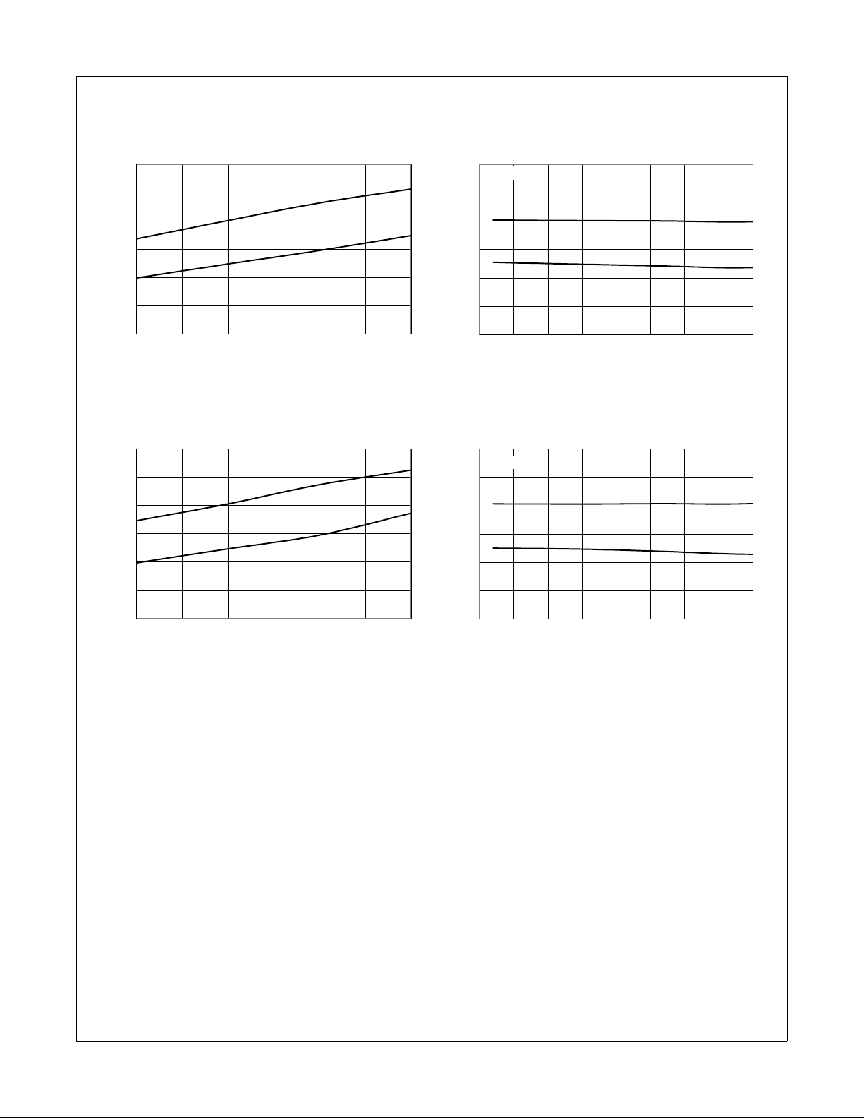
Typical Characteristics
1.0
1.2
1.4
1.6
1.8
2.0
2.2
4.5 4.8 5.0 5.3 5.5 5.8 6.0
Driver Supply Voltage, V
SMOD# Threshold Voltage, V
V
IH
V
IL
1.0
1.2
1.4
1.6
1.8
2.0
2.2
-50 -25 0 25 50 75 100 125 150
Temperature, oC
SMOD# Threshold Voltage, V
V
IH
V
IL
V
CIN
= 5 V
1.0
1.2
1.4
1.6
1.8
2.0
2.2
4.5 4.8 5.0 5.3 5.5 5.8 6.0
Driver Supply Voltage, V
DISB# Threshold Voltage, V
V
IH
V
IL
1.0
1.2
1.4
1.6
1.8
2.0
2.2
-50 -25 0 25 50 75 100 125 150
Temperature, oC
DISB# Threshold Voltage, V
V
IH
V
IL
V
CIN
= 5 V
VIN = 12V, V
Figure 19. SMOD# Threshold Voltage vs. Driver Supply Voltage Figure 20. SMOD# Threshold Voltage vs. Temperature
= 5V, TA = 25°C unless otherwise noted.
CIN
FDMF6704A
The Xtra Small, High Performance, High Frequency DrMOS Module
Figure 21. DISB# Threshold Voltage vs. Driver Supply Voltage
FDMF6704A Rev. F
Figure 22. DISB# Threshold Voltage vs. Temperature
9
www.fairchildsemi.com
Page 10
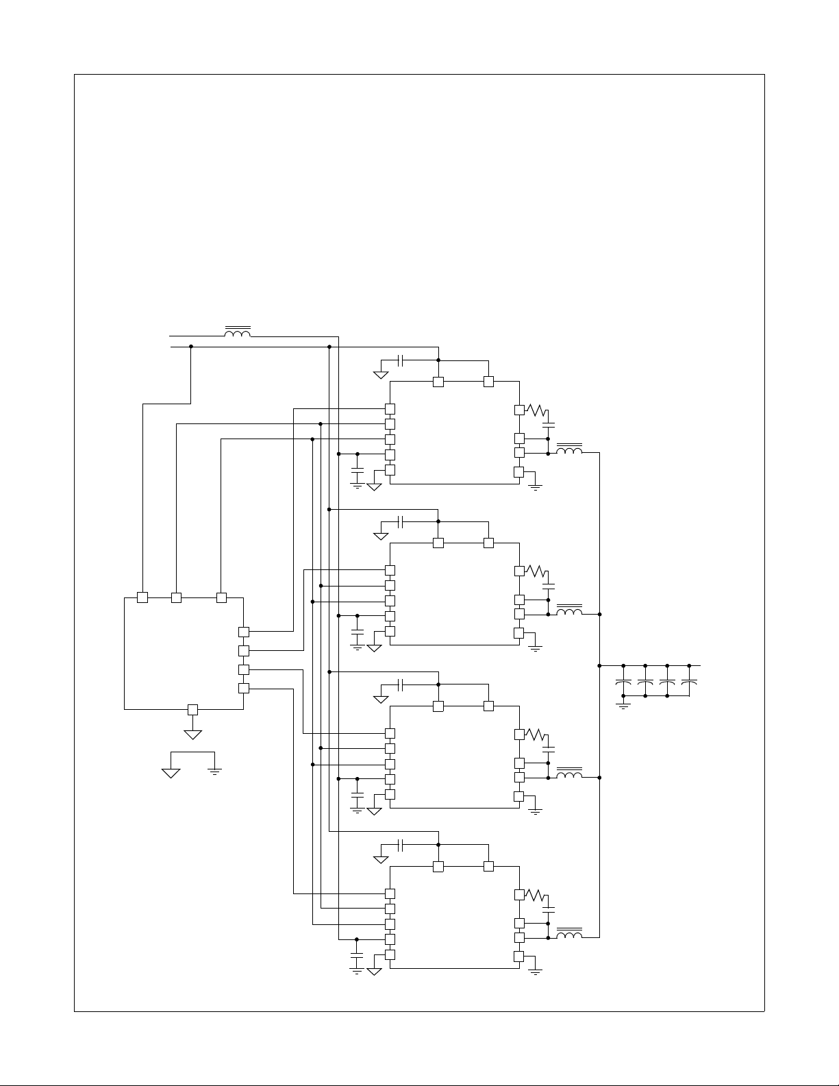
Application Information
Supply Capacitor Selection
For the supply input (VCIN) of the FDMF6704A, a local ceramic
bypass capacitor is recommended to reduce the noise and to
supply the peak current. Use at least a 1F, X7R or X5R
capacitor. Keep this capacitor close to the FDMF6704A VCIN
and PGND pins.
Bootstrap Circuit
The bootstrap circuit uses a charge storage capacitor (C
as shown in Figure 23. A bootstrap capacitance of 100nF, X7R
or X5R capacitor is adequate. A series bootstrap resistor would
be needed for specific application in order to improve switching
noise immunity.
BOOT
Typical Application
VIN 12V
V5V 5V
VCIN Filter
The VDRV pin provides power to the gate drive of the high side
and low side power FET. In most cases, it can be connected
directly to VCIN, the pin that provides power to the logic section
of the driver. For additional noise immunity, an RC filter can be
inserted between VDRV and VCIN. Recommended values
would be 10 Ohms and 1F.
),
FDMF6704A
The Xtra Small, High Performance, High Frequency DrMOS Module
VCC
PWM
Controller
Signal
GND
EN
CGND
SMOD#
PWM1
PWM2
PWM3
PWM4
Power
GND
VDRV
PWM
DISB#
SMOD#
VIN
CGND
FDMF6704A
VDRV
PWM
DISB#
SMOD#
VIN
CGND
FDMF6704A
VDRV
PWM
DISB#
SMOD#
VIN
CGND
FDMF6704A
VCIN
BOOT
PHASE
VSWH
PGND
VCIN
BOOT
PHASE
VSWH
PGND
VCIN
BOOT
PHASE
VSWH
PGND
R
R
R
BOOT
BOOT
BOOT
C
L
C
L
C
L
BOOT
OUT
BOOT
OUT
BOOT
OUT
V
OUT
FDMF6704A Rev. F
VDRV
PWM
DISB#
SMOD#
VIN
CGND
FDMF6704A
Figure 23. Typical Application
10
VCIN
BOOT
PHASE
VSWH
PGND
R
BOOT
C
L
BOOT
OUT
www.fairchildsemi.com
Page 11
FDMF6704A
Power Loss and Efficiency
Measurement and Calculation
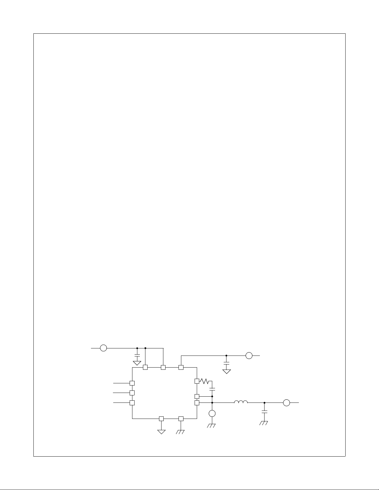
Refer to Figure 24 for power loss testing method. Power loss
calculation are as follows:
(a) PIN = (VIN x IIN) + (V5V x I5V) (W)
(b) PSW = VSW x I
(c) P
(d) P
(e) P
(f) EFF
(g) EFF
= V
OUT
LOSS_MODULE
LOSS_BOARD
= 100 x PSW/P
MODULE
= 100 x P
BOARD
OUT
= PIN - PSW (W)
= PIN - P
(W)
OUT
x I
(W)
OUT
OUT
IN
OUT/PIN
(W)
(%)
(%)
PCB Layout Guideline
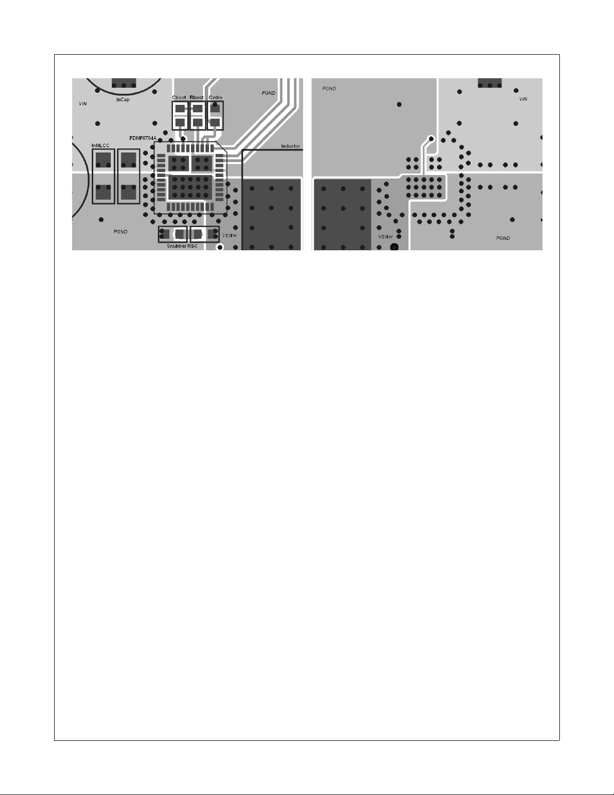
Figure 25 shows a proper layout example of FDMF6704A and
critical parts. All of high current flow path, such as VIN, VSWH,
V
and GND copper, should be short and wide for better and
OUT
stable current flow, heat radiation and system performance.
Following is a guideline which the PCB designer should
consider:
1. Input ceramic bypass capacitors must be close to VIN and
PGND pin of FDMF6704A to help reduce the input current ripple
component induced by switching operation.
2. The VSWH copper trace serves two purposes. In addition to
being the high frequency current path from the DrMOS package
to the output inductor, it also serves as heatsink for the lower
FET in the DrMOS package. The trace should be short and wide
enough to present a low impedance path for the high frequency,
high current flow between the DrMOS and inductor in order to
minimize losses and temperature rise. Please note that the
VSWH node is a high voltage and high frequency switching
node with high noise potential. Care should be taken to
minimize coupling to adjacent traces. Additionally, since this
copper trace also acts as heatsink for the lower FET, tradeoff
must be made to use the largest area possible to improve
DrMOS cooling while maintaining acceptable noise emission.
3. Output inductor location should be as close as possible to the
FDMF6704A for lower power loss due to copper trace. Care
should be taken so that inductor dissipation does not heat the
DrMOS.
4. The PowerTrench
very effective at minimizing ringing. In most cases, no snubber
will be required. If a snubber is used, it should be placed near
®
5 MOSFETs used in the output stage are
the FDMF6704A. The resistor and capacitor need to be of
proper size for the power dissipation.
5. Place ceramic bypass capacitor and BOOT capacitor as
close as possible to the VCIN and BOOT pins of the
FDMF6704A to ensure clean and stable power. Routing width
and length should be considered as well.
6. Include a trace from PHASE to VSWH in order to improve
noise margin. Keep the trace as short as possible.
7. The layout should include the option to insert a small value
series boot resistor between boot cap and BOOT pin. The boot
loop size, including Rboot and Cboot, should be as small as
possible. The boot resistor is normally not required, but is
effective at improving noise operating margin in multi phase
designs that may have noise issues due to ground bounce and
high negative VSWH ringing. The VIN and PGND pins handle
large current transients with frequency components above
100 MHz. If possible, these package pins should be connected
directly to the VIN and board GND planes. The use of thermal
relief traces in series with these pins is discouraged since this
will add inductance to the power path. This added inductance in
series with the PGND pin will degrade system noise immunity
by increasing negative VSWH ringing.
8. CGND pad and PGND pins should be connected by plane
GND copper with multiple vias for stable grounding. Poor
grounding can create a noise transient offset voltage level
between CGND and PGND. This could lead to fault operation of
gate driver and MOSFET.
9. Ringing at the BOOT pin is most effectively controlled by
close placement of the boot capacitor. Do not add an additional
BOOT to PGND capacitor. This may lead to excess current flow
through the BOOT diode.
10. SMOD#, DISB# and PWM pins don’t have internal pull up or
pull down resistors. They should not be left floating. These pins
should not have any noise filter caps.
11. Use multiple vias on each copper area to interconnect top,
inner and bottom layers to help smooth current flow and heat
conduction. Vias should be relatively large and of reasonable
inductance. Critical high frequency components such as Rboot,
Cboot, the RC snubber and bypass caps should be located
close to the DrMOS module and on the same side of the PCB
as the module. If not feasible, they should be connected from
the backside via a network of low inductance vias.
The Xtra Small, High Performance, High Frequency DrMOS Module
FDMF6704A Rev. F
V
5V
PWM Input
SMOD#
A
DISB#
I
5V
C
VDRV
VDRV
DISB#
PWM
SMOD#
VCIN
VIN
BOOT
PHASE
VSWH
R
BOOT
CGND PGND
Figure 24. Power Loss Measurement Block Diagram
11
I
IN
V
A
IN
C
VIN
C
BOOT
L
OUT
V
V
SW
C
I
OUT
OUT
V
A
OUT
www.fairchildsemi.com
Page 12
FDMF6704A
The Xtra Small, High Performance, High Frequency DrMOS Module
TOP VIEW
BOTTOM VIEW
Figure 25. Typical PCB Layout Example
FDMF6704A Rev. F
12
www.fairchildsemi.com
Page 13
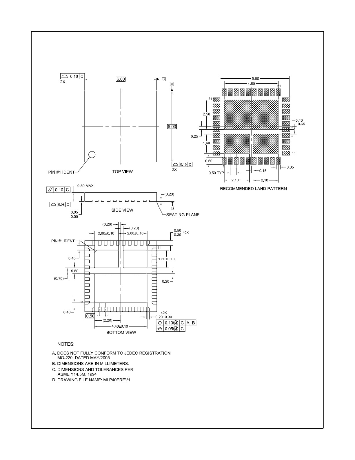
Dimensional Outline and Pad layout
FDMF6704A
The Xtra Small, High Performance, High Frequency DrMOS Module
FDMF6704A Rev. F
13
www.fairchildsemi.com
Page 14
FDMF6704A
TRADEMARKS
The following includes registered and unregistered trademarks and service marks, owned by Fairchild Semiconductor and/or its global subsidianries, and is
not intended to be an exhaustive list of all such trademarks.
Auto-SPM™
Build it Now™
CorePLUS™
CorePOWER™
CROSSVOLT™
CTL™
Current Transfer Logic™
EcoSPARK
®
EfficentMax™
EZSWITCH™*
™*
®
Fairchild
Fairchild Semiconductor
FACT Quiet Series™
®
FACT
®
FAST
FastvCore™
FETBench™
FlashWriter®*
FPS™
F-PFS™
®
FRFET
Global Power Resource
Green FPS™
Green FPS™ e-Series™
SM
Gmax™
GTO™
IntelliMAX™
ISOPLANAR™
MegaBuck™
MICROCOUPLER™
MicroFET™
MicroPak™
MillerDrive™
®
MotionMax™
Motion-SPM™
OPTOLOGIC
OPTOPLANAR
®
PDP SPM™
Power-SPM™
®
®
PowerTrench
PowerXS™
Programmable Active Droop™
QFET
QS™
Quiet Series™
RapidConfigure™
Saving our world, 1mW/W/kW at a time™
SmartMax™
SMART START™
SPM
STEALTH™
SuperFET™
SuperSOT™-3
SuperSOT™-6
SuperSOT™-8
SupreMOS™
SyncFET™
Sync-Lock™
®
®
The Power Franchise
TinyBoost™
TinyBuck™
TinyLogic
®
TINYOPTO™
TinyPower™
TinyPWM™
TinyWire™
TriFault Detect™
®
TRUECURRENT™*
µSerDes™
®
UHC
Ultra FRFET™
UniFET™
VCX™
®
*
VisualMax™
XS™
®
* Trademarks of System General Corporation, used under license by Fairchild Semiconductor.
DISCLAIMER
FAIRCHILD SEMICONDUCTOR RESERVES THE RIGHT TO MAKE CHANGES WITHOUT FURTHER NOTICE TO ANY PRODUCTS HEREIN TO IMPROVE
RELIABILITY, FUNCTION, OR DESIGN. FAIRCHILD DOES NOT ASSUME ANY LIABILITY ARISING OUT OF THE APPLICATION OR USE OF ANY
PRODUCT OR CIRCUIT DESCRIBED HEREIN; NEITHER DOES IT CONVEY ANY LICENSE UNDER ITS PATENT RIGHTS, NOR THE RIGHTS OF OTHERS.
THESE SPECIFICATIONS DO NOT EXPAND THE TERMS OF FAIRCHILD°ØS WORLDWIDE TERMS AND CONDITIONS, SPECIFICALLY THE WARRANTY
THEREIN, WHICH COVERS THESE PRODUCTS.
LIFE SUPPORT POLICY
FAIRCHILD’S PRODUCTS ARE NOT AUTHORIZED FOR USE AS CRITICAL COMPONENTS IN LIFE SUPPORT DEVICES OR SYSTEMS WITHOUT THE
EXPRESS WRITTEN APPROVAL OF FAIRCHILD SEMICONDUCTOR CORPORATION.
As used herein:
1. Life support devices or systems are devices or systems which, (a) are
intended for surgical implant into the body or (b) support or sustain life,
and (c) whose failure to perform when properly used in accordance with
instructions for use provided in the labeling, can be reasonably
2. A critical component in any component of a life support, device, or
system whose failure to perform can be reasonably expected to cause
the failure of the life support device or system, or to affect its safety or
effectiveness.
expected to result in a significant injury of the user.
ANTI-COUNTERFEITING POLICY
Fairchild Semiconductor Corporation's Anti-Counterfeiting Policy. Fairchild's Anti-Counterfeiting Policy is also stated on our external website,
www.fairchildsemi.com, under Sales Support.
Counterfeiting of semiconductor parts is a growing problem in the industry. All manufacturers of semiconductor products are experiencing counterfeiting of
their parts. Customers who inadvertently purchase counterfeit parts experience many problems such as loss of brand reputation, substandard performance,
failed applications, and increased cost of production and manufacturing delays. Fairchild is taking strong measures to protect ourselves and our customers
from the proliferation of counterfeit parts. Fairchild strongly encourages customers to purchase Fairchild parts either directly from Fairchild or from Authorized
Fairchild Distributors who are listed by country on our web page cited above. Products customers buy either from Fairchild directly or from Authorized Fairchild
Distributors are genuine parts, have full traceability, meet Fairchild's quality standards for handling and storage and provide access to Fairchild's full range of
up-to-date technical and product information. Fairchild and our Authorized Distributors will stand behind all warranties and will appropriately address any
warranty issues that may arise. Fairchild will not provide any warranty coverage or other assistance for parts bought from Unauthorized Sources. Fairchild is
committed to combat this global problem and encourage our customers to do their part in stopping this practice by buying direct or from authorized distributors.
The Xtra, Small High Performance, High Frequency DrMOS Module
PRODUCT STATUS DEFINITIONS
Definition of Terms
Datasheet Identification Product Status Definition
Advance Information Formative / In Design
Preliminary First Production
No Identification Needed Full Production
Obsolete Not In Production
Datasheet contains the design specifications for product development. Specifications may change
in any manner without notice.
Datasheet contains preliminary data; supplementary data will be published at a later date. Fairchild
Semiconductor reserves the right to make changes at any time without notice to improve design.
Datasheet contains final specifications. Fairchild Semiconductor reserves the right to make
changes at any time without notice to improve the design.
Datasheet contains specifications on a product that is discontinued by Fairchild Semiconductor.
The datasheet is for reference information only.
14
FDMF6704A Rev. F
Rev. I40
www.fairchildsemi.com
 Loading...