

Page 1
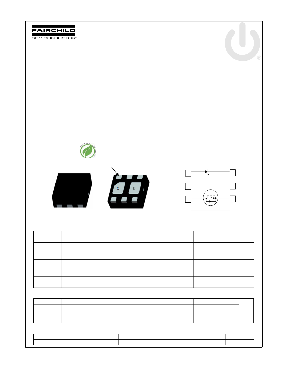
FDFMA2P859T Integrated P-Channel PowerTrench
FDFMA2P859T
July 2009
Integrated P-Channel PowerTrench® MOSFET and Schottky Diode
–20 V, –3.0 A, 120 m:
Features
MOSFET:
Max r
Max r
Max r
Schottky:
VF < 0.54 V @ 1 A
Low profile - 0.55 mm maximum - in the new package
MicroFET 2x2 Thin
Free from halogenated compounds and antimony oxides
RoHS compliant
= 120 m: at VGS = –4.5 V, ID = –3.0 A
DS(on)
= 160 m: at VGS = –2.5 V, ID = –2.5 A
DS(on)
= 240 m: at VGS = –1.8 V, ID = –1.0 A
DS(on)
Pin 1
A
NC
General Description
This device is designed specifically as a single package solution
for the battery charge switch in cellular handset and other
ultra-portable applications. It features a MOSFET with low
on-state resistance and an independently connected low forward
voltage schottky diode for minimum conduction losses.
The MicroFET 2x2 Thin package offers exceptional thermal
performance for its physical size and is well suited to linear mode
applications.
D
1
A
2
NC
6
5
C
®
MOSFET and Schottky Diode
G
3
D
C
S
G
4
MicroFET 2x2 Thin
MOSFET Maximum Ratings T
Symbol Parameter Ratings Units
V
V
I
P
T
V
I
DSS
GSS
D
D
J
RRM
O
, T
STG
Drain to Source Voltage 20 V
Gate to Source Voltage ±8 V
Drain Current -Continuous (Note 1a) –3
-Pulsed –6
Power Dissipation (Note 1a) 1.4
Power Dissipation (Note 1b) 0.7
Operating and Storage Junction Temperature Range –55 to +150 °C
Schottky Repetitive Peak Reverse Voltage 30 V
Schottky Average Forward Current 1 A
= 25 °C unless otherwise noted
A
Thermal Characteristics
R
TJA
R
TJA
R
TJA
R
TJA
Thermal Resistance, Junction to Ambient (Note 1a) 86
Thermal Resistance, Junction to Ambient (Note 1b) 173
Thermal Resistance, Junction to Ambient (Note 1c) 86
Thermal Resistance, Junction to Ambient (Note 1d) 140
Package Marking and Ordering Information
S
A
W
°C/W
Device Marking Device Package Reel Size Tape Width Quantity
59 FDFMA2P859T MicroFET 2x2 Thin 7 ’’ 8 mm 3000 units
©2009 Fairchild Semiconductor Corporation
FDFMA2P859T Rev.B
1
www.fairchildsemi.com
Page 2
FDFMA2P859T Integrated P-Channel PowerTrench
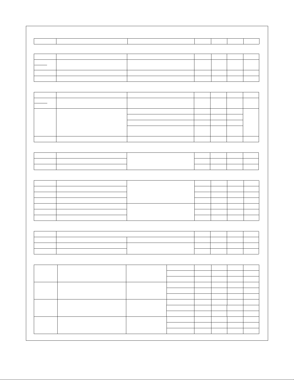
Electrical Characteristics T
= 25 °C unless otherwise noted
J
Symbol Parameter Test Conditions Min Typ Max Units
Off Characteristics
BV
'BV
'T
I
DSS
I
GSS
DSS
DSS
J
Drain to Source Breakdown Voltage ID = –250 PA, VGS = 0 V –20 V
Breakdown Voltage Temperature
Coefficient
I
= –250 PA, referenced to 25 °C –12 mV/°C
D
Zero Gate Voltage Drain Current VDS = –16 V, VGS= 0 V –1 PA
Gate to Source Leakage Current VGS = ±8 V, VDS= 0 V ±100 nA
On Characteristics
V
GS(th)
'V
'T
r
DS(on)
g
FS
GS(th)
J
Gate to Source Threshold Voltage VGS = VDS, ID = –250 PA –0.4 –0.7 –1.3 V
Gate to Source Threshold Voltage
Temperature Coefficient
Static Drain to Source On Resistance
I
= –250 PA, referenced to 25 °C 2 mV/°C
D
V
= –4.5 V, ID = –3.0 A 90 120
GS
= –2.5 V, ID = –2.5 A 120 160
V
GS
= –1.8 V, ID = –1.0 A 172 240
V
GS
= –4.5 V, ID = –3.0 A
V
GS
T
= 125 °C
J
118 160
Forward Transconductance VDS = –5 V, ID = –3.0 A 7 S
Dynamic Characteristics
C
iss
C
oss
C
rss
Input Capacitance
Output Capacitance 80 pF
Reverse Transfer Capacitance 45 pF
= –10 V, VGS = 0 V,
V
DS
f = 1.0 MHz
435 pF
m:
Switching Characteristics
t
d(on)
t
r
t
d(off)
t
f
Q
g(TOT)
Q
gs
Q
gd
Turn-On Delay Time
Rise Time 11 19 ns
Turn-Off Delay Time 15 27 ns
Fall Time 612ns
Total Gate Charge
Gate to Source Gate Charge 0.8 nC
Gate to Drain “Miller” Charge 0.9 nC
Drain-Source Diode Characteristics
I
S
V
SD
t
rr
Q
rr
Maximum Continuous Drain-Source Diode Forward Current –1.1 A
Source to Drain Diode Forward Voltage VGS= 0 V, IS= –1.1 A (Note 2) –0.8 –1.2 V
Reverse Recovery Time
Reverse Recovery Charge 6 nC
Schottky Diode Characteristics
I
R
I
R
V
F
V
F
Reverse Leakage VR = 10 V
Reverse Leakage VR = 20 V
Forward Voltage IF = 100 mA
Forward Voltage IF = 1 A
= –10 V, ID = –1.0 A
V
DD
V
= –4.5 V, R
GS
= –10 V, ID = –3.0 A
V
DD
V
= –4.5 V
GS
= –3.0 A, di/dt = 100 A/Ps
I
F
GEN
= 6 :
918ns
46nC
17 ns
T
= 25 °C 0.3 1.0 PA
J
= 85 °C 25 40 PA
T
J
= 125 °C 0.28 0.37 mA
T
J
T
= 25 °C 1.0 2.5 PA
J
= 85 °C 74 110 PA
T
J
= 125 °C 0.73 1.00 mA
T
J
T
= 25 °C 0.40 0.41 V
J
= 85 °C 0.31 0.33 V
T
J
= 125 °C 0.26 0.27 V
T
J
T
= 25 °C 0.52 0.54 V
J
= 85 °C 0.45 0.47 V
T
J
= 125 °C 0.41 0.43 V
T
J
®
MOSFET and Schottky Diode
©2009 Fairchild Semiconductor Corporation
FDFMA2P859T Rev.B
2
www.fairchildsemi.com
Page 3
FDFMA2P859T Integrated P-Channel PowerTrench
Electrical Characteristics T
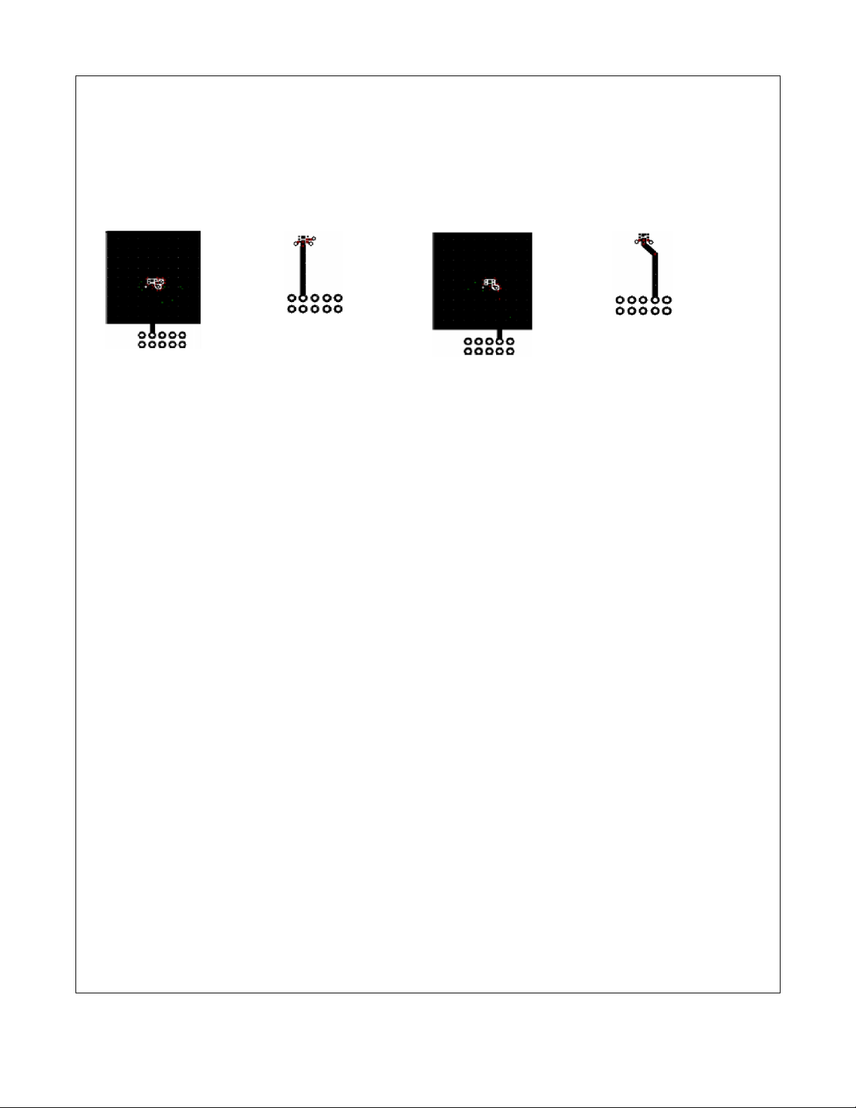
Notes:
1: R
is determined with the device mounted on a 1 in2 oz. copper pad on a 1.5 x 1.5 in. board of FR-4 material. R
TJA
user's board design.
(a) MOSFET R
(b) MOSFET R
(c) Schottky R
(d) Schottky R
2: Pulse Test: Pulse Width < 300 Ps, Duty cycle < 2.0%.
= 86 oC/W when mounted on a 1 in2pad of 2 oz copper, 1.5 ” x 1.5 ” x 0.062 ” thick PCB.
TJA
= 173 oC/W when mounted on a minimum pad of 2 oz copper.
TJA
= 86 oC/W when mounted on a 1 in2pad of 2 oz copper, 1.5 ” x 1.5 ” x 0.062 ” thick PCB.
TJA
= 140 oC/W when mounted on a minimum pad of 2 oz copper.
TJA
a)86 oC/W when
mounted on a 1
in2pad of 2 oz
copper.
= 25 °C unless otherwise noted
A
b)173 oC/W when
mounted on a
minimum pad of 2
oz copper.
is guaranteed by design while R
TJC
c)86 oC/W when
mounted on a 1
in2pad of 2 oz
copper.
is determined by the
TCA
d)140 oC/W when
mounted on a
minimum pad of 2
oz copper.
®
MOSFET and Schottky Diode
©2009 Fairchild Semiconductor Corporation
FDFMA2P859T Rev.B
3
www.fairchildsemi.com
Page 4
FDFMA2P859T Integrated P-Channel PowerTrench
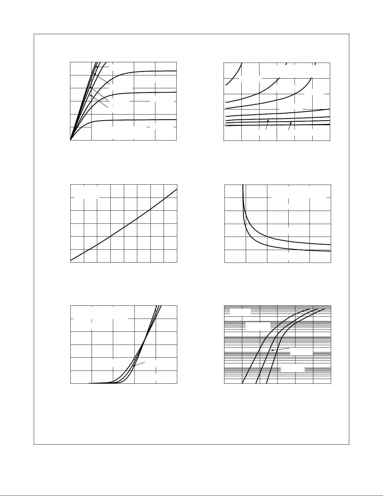
Typical Characteristics T
6
5
4
3
DRAIN CURRENT (A)
2
,
D
-I
1
0
0 0.5 1.0 1.5 2.0 2.5
-V
DS
Figure 1.
1.4
ID = -3.0 A
V
= -4.5 V
GS
1.3
1.2
1.1
1.0
NORMALIZED
0.9
DRAIN TO SOURCE ON-RESISTANCE
0.8
-50 -25 0 25 50 75 100 125 150
T
F i g u r e 3 . N o r m a l i z e d O n - R e s i s t a n c e
vs Junction Temperature
VGS = -4.5 V
VGS = -3.5 V
VGS = -3 V
VGS = -2.5 V
PULSE DURATION = 300 Ps
DUTY CYCLE = 2% MAX
,
DRAIN TO SOURCE VOLTAGE (V)
On-Region Characteristics Figure 2.
,
JUNCTION TEMPERATURE
J
= 25 °C unless otherwise noted
J
VGS = -2 V
VGS = -1.8 V
VGS = -1.5 V
o
(
C
)
3.0
PULSE DURATION = 300 Ps
2.5
VGS = -1.5 V
DUTY CYCLE = 2%MAX
VGS = -1.8 V
2.0
V
= -2.5 V
1.5
NORMALIZED
GS
1.0
DRAIN TO SOURCE ON-RESISTANCE
0.5
0123456
VGS = -3 V
-I
,
DRAIN CURRENT (A)
D
VGS= -3.5 V
N o r m a l i z e d O n - R e s i s t a n c e
vs Drain Current and Gate Voltage
DRAIN TO
,
DS(on)
r
0.28
)
:
0.24
(
0.20
0.16
0.12
0.08
SOURCE ON-RESISTANCE
0.04
0246810
-V
,
GATE TO SOURCE VOLTAGE (V)
GS
Figure 4.
O n - R es i s t a n c e vs G a t e t o
PULSE DURATION = 300 Ps
DUTY CYCLE = 2% MAX
ID= -1.5 A
TJ= 125 oC
TJ= 25 oC
Source Voltage
V
V
GS
GS
= -2 V
=-4.5 V
®
MOSFET and Schottky Diode
6
PULSE DURATION = 300 Ps
DUTY CYCLE = 2% MAX
5
VDS= -5 V
4
3
2
, DRAIN CURRENT (A)
D
-I
1
0
0 0.5 1.0 1.5 2.0 2.5
TJ = 125 oC
-VGS, GATE TO SOURCE VOLTAGE (V)
Figure 5. Transfer Characteristics
©2009 Fairchild Semiconductor Corporation
FDFMA2P859T Rev.B
TJ = 25 oC
TJ = -55 oC
10
VGS= 0 V
1
TJ= 125 oC
0.1
0.01
0.001
, REVERSE DRAIN CURRENT (A)
S
-I
0.0001
0 0.2 0.4 0.6 0.8 1.0 1.2
-VSD, BODY DI ODE FORWARD VOLTAGE (V)
Figure 6.
S o u r ce t o D r a i n D io d e
TJ = 25 oC
TJ = -55 oC
Forward Voltage vs Source Current
4
www.fairchildsemi.com
Page 5
FDFMA2P859T Integrated P-Channel PowerTrench
Typical Characteristics T
5
ID= -3.0 A
4
VDD = -5 V
3
2
1
, GATE TO SOURCE VOLTAGE (V)
GS
-V
0
012345
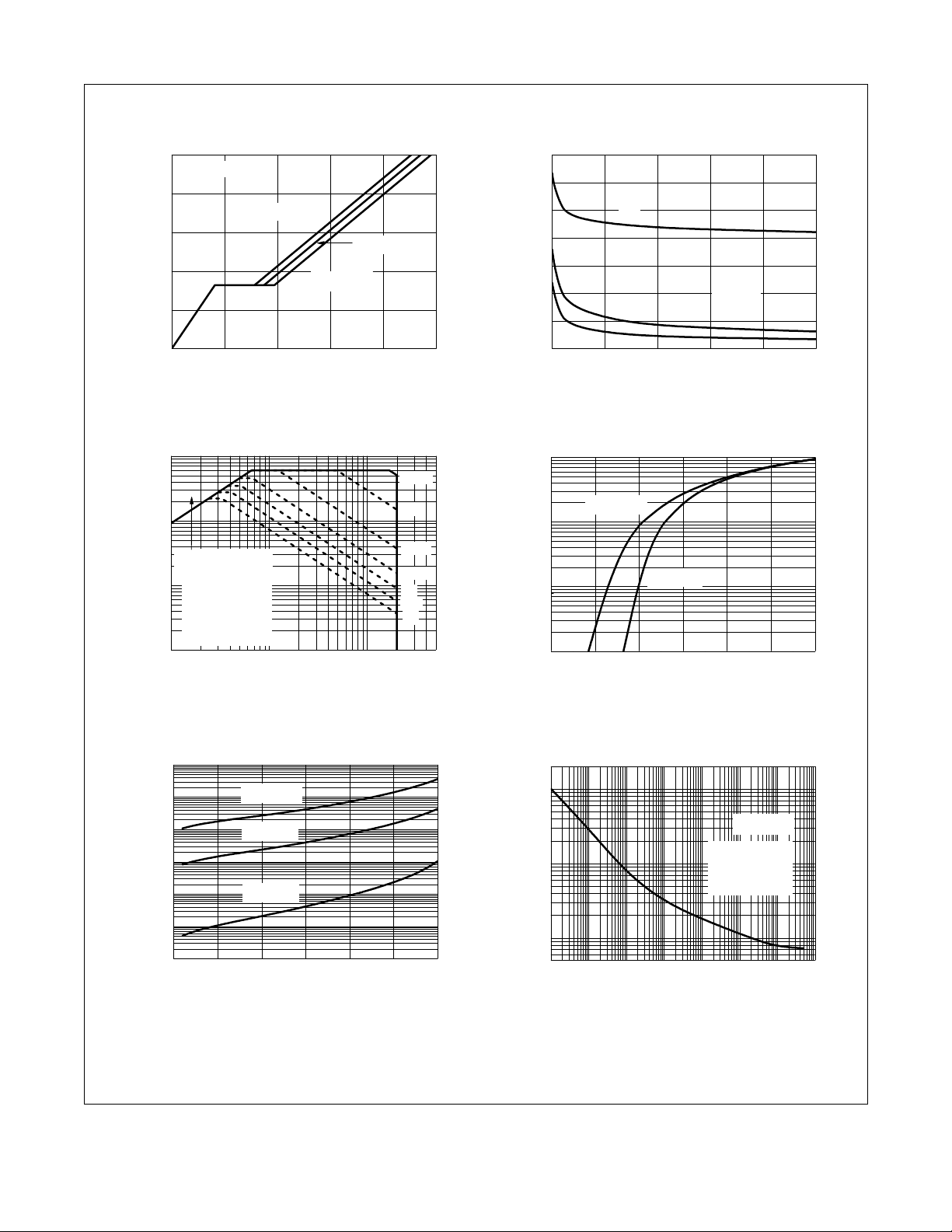
Qg, GATE CHARGE (nC)
Figure 7.
10
1
0.1
, DRAIN CURRENT (A)
D
-I
0.01
0.1 1 10
Gate Charge Characteristics Figure 8.
THIS AREA IS
LIMITED BY r
SINGLE PULSE
T
R
T
F i g u re 9 .
DS(on)
= MAX RATED
J
= 173 oC/W
T
JA
= 25 oC
A
-VDS, DRAIN to SOURCE VOLTAGE (V)
F o r w ar d B i a s S a fe
Operating Area
= 25 °C unless otherwise noted
J
VDD = -10 V
VDD= -15 V
100 us
1 ms
10 ms
100 ms
1 s
10 s
DC
50
700
600
500
C
iss
400
300
200
CAPACITANCE (pF)
C
oss
100
C
rss
0
048121620
-VDS, DRAIN TO SOURCE VOLTAGE (V)
f = 1 MHz
V
= 0 V
GS
C a p a c i t a n c e v s D r a i n
to Source Voltage
10
TJ= 125 oC
1
0.1
FORWARD CURRENT (A)
,
F
I
0.01
0 0.2 0.4 0.6 0.8 1.0 1.2
Figure 10.
Schottky Diode Foward Volta ge
TJ= 25 oC
V
FORWARD V OLTAG E (V)
F
,
®
MOSFET and Schottky Diode
10000
1000
100
TJ= 125 oC
TJ = 85 oC
10
1
TJ = 25 oC
0.1
REVERSE LEAKAGE CURRENT (mA)
,
R
I
0.01
0 5 10 15 20 25 30
Figure 11.
©2009 Fairchild Semiconductor Corporation
FDFMA2P859T Rev.B
V
,
REVERSE VOLTAGE (V)
R
Schottky Diode Reverse Current Figure 12.
200
100
VGS = -10 V
10
PEAK TRANSIENT POWER (W)
,
)
1
PK
(
P
0.5
10-410-310-210-1110
t, PULSE WIDTH (sec)
SINGLE PULSE
= 173 oC/W
R
T
JA
T
= 25 oC
A
100 1000
S i n g l e P u l s e M a x i m u m
Power Dissipation
5
www.fairchildsemi.com
Page 6
FDFMA2P859T Integrated P-Channel PowerTrench
Typical Characteristics T
2
1
JA
T
0.1
IMPEDANCE, Z
NORMALIZED THERMAL
0.01
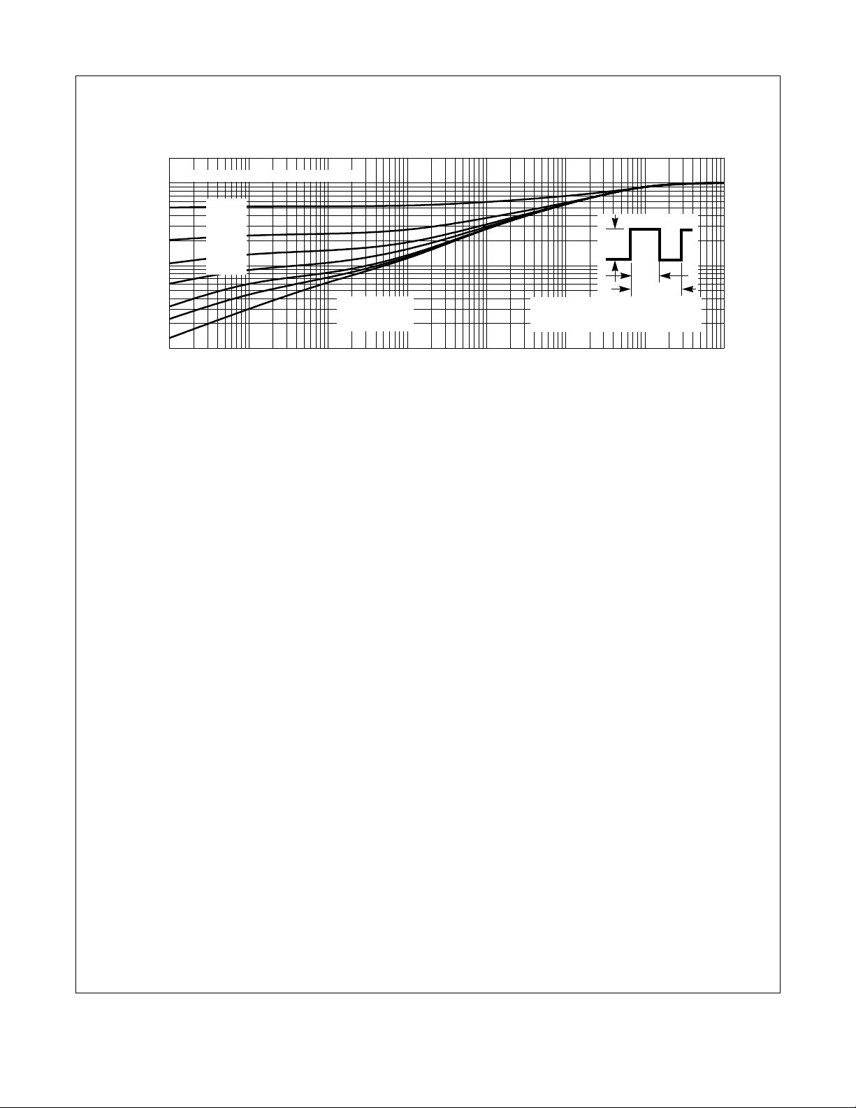
DUTY CYCLE-DESCENDING ORDER
D = 0.5
0.2
0.1
0.05
0.02
0.01
-4
10
-3
10
Figure 13. Junction to Ambient Transient Thermal Response Curve
= 25 °C unless otherwise noted
J
SINGLE PULSE
R
= 173 oC/W
T
JA
-2
10
t, RECTANGULAR PULSE DURATION (sec)
-1
10
P
DM
NOTES:
DUTY FACTOR: D = t1/t
PEAK TJ = PDM x Z
TJA
x R
2
110
t
1
t
2
+ T
TJA
A
100 1000
®
MOSFET and Schottky Diode
©2009 Fairchild Semiconductor Corporation
FDFMA2P859T Rev.B
6
www.fairchildsemi.com
Page 7
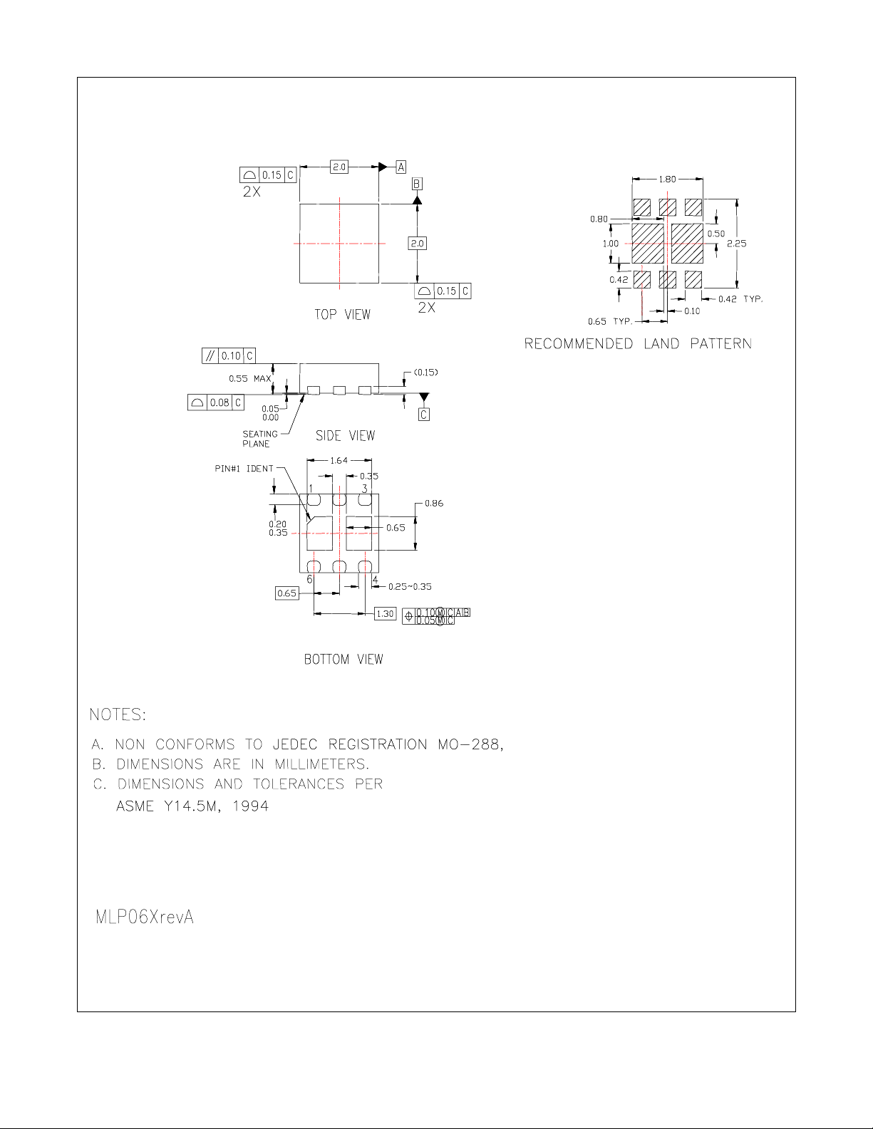
Dimensional Outline and Pad Layout
FDFMA2P859T Integrated P-Channel PowerTrench
®
MOSFET and Schottky Diode
©2009 Fairchild Semiconductor Corporation
FDFMA2P859T Rev.B
7
www.fairchildsemi.com
Page 8
TRADEMARKS
®
t
m
The following includes registered and unregistered trademarks and service marks, owned by Fairchild Semiconductor and/or its global subsidiaries, and is not
intended to be an exhaustive list of all such trademarks.
AccuPower™
Auto-SPM™
Build it Now™
CorePLUS™
CorePOWER™
CROSSVOLT™
CTL™
Current Transfer Logic™
EcoSPARK
EfficentMax™
EZSWITCH™*
™*
Fairchild
Fairchild Semiconductor
FACT Quiet Series™
FACT
FAST
FastvCore™
FETBench™
FlashWriter
®
®
®
®
®
*
®
FPS™
F-PFS™
FRFET
Global Power Resource
Green FPS™
Green FPS™ e-Series™
Gmax™
GTO™
IntelliMAX™
ISOPLANAR™
MegaBuck™
MICROCOUPLER™
MicroFET™
MicroPak™
MillerDrive™
MotionMax™
Motion-SPM™
OPTOLOGIC
OPTOPLANAR
®
m
PDP SPM™
Power-SPM™
PowerTrench
®
SM
PowerXS™
Programmable Active Droop™
QFET
QS™
Quiet Series™
RapidConfigure™
Saving our world, 1mW /W /kW at a time™
SmartMax™
SMART START™
SPM
STEALTH™
SuperFET™
SuperSOT™-3
®
®
SuperSOT™-6
SuperSOT™-8
SupreMOS™
SyncFET™
Sync-Lock™
®
®
™
®
The Power Franchise
TinyBoost™
TinyBuck™
TinyCalc™
TinyLogic
TINYOPTO™
TinyPower™
TinyPWM™
TinyWire™
TriFault Detect™
®
t
®
®
TRUECURRENT™*
®
UHC
Ultra FRFET™
UniFET™
VCX™
VisualMax™
®*
XS™
*Trademarks of System General Corporation, used under license by Fairchild Semiconductor.
DISCLAIMER
FAIRCHILD SEMICONDUCTOR RESERVES THE RIGHT TO MAKE CHANGES WITHOUT FURTHER NOTICE TO ANY PRODUCTS HEREIN TO IMPROVE
RELIABILITY, FUNCTION, OR DESIGN. FAIRCHILD DOES NOT ASSUME ANY LIABILITY ARISING OUT OF THE APPLICATION OR USE OF ANY
PRODUCT OR CIRCUIT DESCRIBED HEREIN; NEITHER DOES IT CONVEY ANY LICENSE UNDER ITS PATENT RIGHTS, NOR THE RIGHTS OF OTHERS.
THESE SPECIFICATIONS DO NOT EXPAND THE TERMS OF FAIRCHILD’S WORLDWIDE TERMS AND CONDITIONS, SPECIFICALLY THE WARRANTY
THEREIN, WHICH COVERS THESE PRODUCTS.
FDFMA2P859T Integrated P-Channel PowerTrench
®
MOSFET and Schottky Diode
LIFE SUPPORT POLICY
FAIRCHILD’S PRODUCTS ARE NOT AUTHORIZED FOR USE AS CRITICAL COMPONENTS IN LIFE SUPPORT DEVICES OR SYSTEMS WITHOUT THE
EXPRESS WRITTEN APPROVAL OF FAIRCHILD SEMICONDUCTOR CORPORATION.
As used herein:
1. Life support devices or systems are devices or systems which, (a) are
intended for surgical implant into the body or (b) support or sustain life,
and (c) whose failure to perform when properly used in accordance with
instructions for use provided in the labeling, can be reasonably
expected to result in a significant injury of the user.
ANTI-COUNTERFEITING POLICY
Fairchild Semiconductor Corporation’s Anti-Counterfeiting Policy. Fairchild’s Anti-Counterfeiting Policy is also stated on our external website,
www.Fairchildsemi.com, under Sales Support
Counterfeiting of semiconductor parts is a growing problem in the industry. All manufactures of semiconductor products are experiencing counterfeiting of their
parts. Customers who inadvertently purchase counterfeit parts experience many problems such as loss of brand reputation, substandard performance, failed
application, and increased cost of production and manufacturing delays. Fairchild is taking strong measures to protect ourselves and our customers from the
proliferation of counterfeit parts. Fairchild strongly encourages customers to purchase Fairchild parts either directly from Fairchild or from Authorized Fairchild
Distributors who are listed by country on our web page cited above. Products customers buy either from Fairchild directly or from Authorized Fairchild
Distributors are genuine parts, have full traceability, meet Fairchild’s quality standards for handing and storage and provide access to Fairchild’s full range of
up-to-date technical and product information. Fairchild and our Authorized Distributors will stand behind all warranties and will appropriately address and
warranty issues that may arise. Fairchild will not provide any warranty coverage or other assistance for parts bought from Unauthorized Sources. Fairchild is
committed to combat this global problem and encourage our customers to do their part in stopping this practice by buying direct or from authorized distributors.
PRODUCT STATUS DEFINITIONS
Definition of Terms
.
2. A critical component in any component of a life support, device, or
system whose failure to perform can be reasonably expected to cause
the failure of the life support device or system, or to affect its safety or
effectiveness.
Datasheet Identification Product Status Definition
Advance Information Formative / In Design
Preliminary First Production
No Identification Needed Full Production
Obsolete Not In Production
©2009 Fairchild Semiconductor Corporation
FDFMA2P859T Rev.B
Datasheet contains the design specifications for product development. Specifications
may change in any manner without notice.
Datasheet contains preliminary data; supplementary data will be published at a later
date. Fairchild Semiconductor reserves the right to make changes at any time without
notice to improve design.
Datasheet contains final specifications. Fairchild Semiconductor reserves the right to
make changes at any time without notice to improve the design.
Datasheet contains specifications on a product that is discontinued by Fairchild
Semiconductor. The datasheet is for reference information only.
Rev. I41
8
www.fairchildsemi.com
 Loading...