

Page 1
o
April 2008
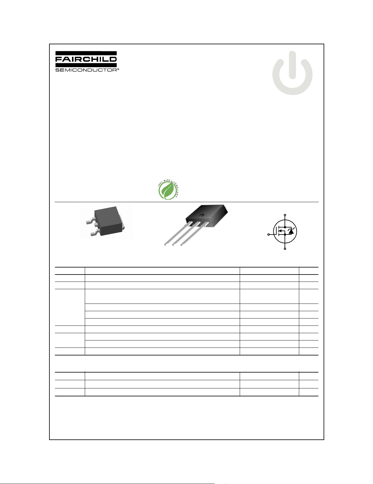
FDD8874 / FDU8874
FDD8874 / FDU8874
N-Channel PowerTrench® MOSFET
30V, 116A, 5.1mΩ
General Description
This N-Channel MOSFET has been designed specifically to
improve the overall efficiency of DC/DC converters using
either synchronous or conventional switching PWM
controllers. It has been optimized for low gate charge, low
r
and fast switching speed.
DS(ON)
Applications
• DC/DC converters
D
G
S
D-PAK
TO-252
(TO-252)
MOSFET Maximum Ratings T
Symbol Parameter Ratings Units
V
V
I
E
P
T
D
DSS
GS
AS
D
, T
J
STG
Drain to Source Voltage 30 V
Gate to Source Voltage ±20 V
Drain Current
Continuous (T
Continuous (T
Continuous (T
Pulsed Figure 4 A
Single Pulse Avalanche Energy (Note 2) 240 mJ
Power dissipation 110 W
Derate above 25
Operating and Storage Te mperature -55 to 175
= 25oC, VGS = 10V) (Note 1)
C
= 25oC, VGS = 4.5V) (Note 1) 103 A
C
= 25oC, VGS = 10V, with R
amb
o
C0.73W/
G DS
= 25°C unless otherwise noted
C
Features
•r
•r
• High performance trench technology for extremely low
• Low gate charge
• High power and current handling capability
• RoHS Compliant
= 52oC/W) 18 A
θJA
= 5.1mΩ, V
DS(ON)
= 6.4mΩ, V
DS(ON)
r
DS(ON)
I-PAK
(TO-251AA)
= 10V, ID = 35A
GS
= 4.5V, ID = 35A
GS
D
G
S
116 A
tm
o
C
o
C
Thermal Characteristics
R
θJC
R
θJA
R
θJA
©2008 Fairchild Semiconductor Corporation
Thermal Resistance Junction to Case TO-252, TO-251 1.36
Thermal Resistance Junction to Ambient TO-252, TO-251 100
Thermal Resistance Junction to Ambient TO-252, 1in2 copper pad area 52
o
C/W
o
C/W
o
C/W
FDD8874 / FDU8874 Rev. B2
Page 2
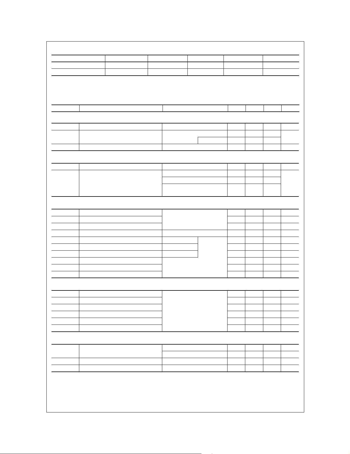
Package Marking and Ordering Information
Device Marking Device Package Reel Size Tape Width Quantity
FDD8874 FDD8874 TO-252AA 13” 12mm 2500 units
FDU8874 FDU8874 TO-251AA Tube N/A (Tube) 75 units
F
F
FDD8874 / FDU8874
Electrical Characteristics
TC = 25°C unless otherwise noted
Symbol Parameter Tes t Cond itions Min Typ Max Units
Off Characteristics
B
VDSS
I
DSS
I
GSS
Drain to Source Breakdown Voltage ID = 250µA, VGS = 0V 30 - - V
V
= 24V - - 1
Zero Gate Voltage Drain Current
DS
= 0V TC = 150oC - - 250
V
GS
Gate to Source Leakage Current VGS = ±20V - - ±100 nA
On Characteristics
V
GS(TH)
r
DS(ON)
Gate to Source Threshold Voltage VGS = VDS, ID = 250µA 1.2 - 2.5 V
I
= 35A, VGS = 10V - 0.0042 0.0051
D
= 35A, VGS = 4.5V - 0.0052 0.0064
I
Drain to Source On Resistance
D
I
= 35A, VGS = 10V,
D
= 175oC
T
J
- 0.0069 0.0083
Dynamic Characteristics
C
ISS
C
OSS
C
RSS
R
G
Q
g(TOT)
Q
g(5)
Q
g(TH)
Q
gs
Q
gs2
Q
gd
Input Capacitance
Output Capacitance - 585 - pF
Reverse Transfer Capacitance - 340 - pF
= 15V, VGS = 0V,
V
DS
f = 1MHz
Gate Resistance VGS = 0.5V, f = 1MHz - 2.0 - Ω
Total Gate Charge at 10V VGS = 0V to 10V
Total Gate Charge at 5V VGS = 0V to 5V - 29 38 nC
V
= 15V
Threshold Gate Charge VGS = 0V to 1V - 3.0 4.0 nC
Gate to Source Gate Charge - 8.0 - nC
Gate Charge Threshold to Plateau - 5.0 - nC
DD
= 35A
I
D
= 1.0mA
I
g
Gate to Drain “Miller” Charge - 10 - nC
- 2990 - pF
-5472nC
µA
Ω
Switching Characteristics
t
ON
t
d(ON)
t
r
t
d(OFF)
t
f
t
OFF
Turn-On Time
Turn-On Delay Time - 9 - ns
Rise Time - 96 - ns
Turn-Off Delay Time - 47 - ns
Fall Time - 37 - n s
Turn-Off Time - - 126 ns
(VGS = 10V)
= 15V, ID = 35A
V
DD
= 10V, RGS = 4.7Ω
V
GS
- - 156 ns
Drain-Source Diode Characteristics
I
= 35A - - 1.25 V
V
SD
t
rr
Q
RR
Notes:
1: Package current limitation is 35A.
2: Starting T
3
©2008 Fairchild Semiconductor Corporation FDD8874 / FDU8874 Rev.B2
Source to Drain Diode Voltage
Reverse Recovery Time ISD = 35A, dISD/dt = 100A/µs- -32ns
Reverse Recovered Charge ISD = 35A, dISD/dt = 100A/µs- -18nC
= 25°C, L = 0.61mH, IAS = 28A, VDD = 27V, VGS = 10V.
J
SD
I
= 15A - - 1.0 V
SD
Page 3
FDD8874 / FDU8874
Typical Characteristics T
= 25°C unless otherwise noted
C
1.2
1.0
0.8
0.6
0.4
0.2
POWER DISSIPATION MULT IPL I ER
0
0 25 50 75 100 175
125
150
TC, CASE TEMPERATURE (oC)
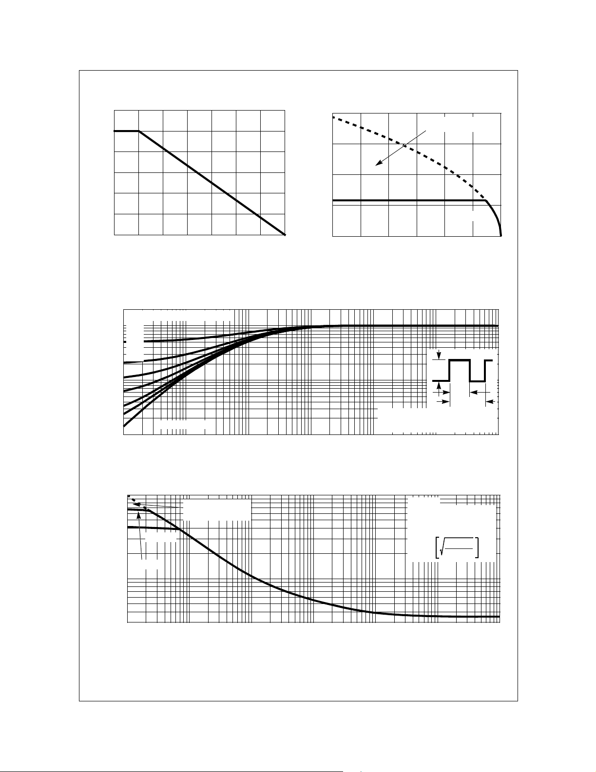
Figure 1. Normali ze d Po we r Dis sip ation vs Case
Temperature
2
DUTY CYCLE - DESCENDING ORDER
0.5
1
0.2
0.1
0.05
0.02
0.01
0.1
, NORMALIZED
θJC
Z
THERMAL IMPEDANCE
0.01
-5
10
SINGLE PULSE
-4
10
-3
10
t, RECTANGULAR PULSE DURATION (s)
120
CURRENT LIMITED
BY PACKAGE
90
60
, DRAIN CURRENT (A)
D
30
I
VGS = 10V
0
25 50 75 100 125 150 175
TC, CASE TEMPERATURE (oC)
Figure 2. Maximum Contin uous Drain Current vs
Case Temperature
P
DM
t
1
t
x R
θJC
+ T
2
C
1
10
NOTES:
DUTY FACTOR: D = t
PEAK TJ = PDM x Z
-2
10
-1
10
θJC
10
1/t2
0
Figure 3. Normalized Maximum Transient Thermal Impedance
1000
TRANSCONDUCTANCE
MAY LIMIT CURRENT
IN THIS REGION
VGS = 4.5V
VGS = 10V
100
, PEAK CURRENT (A)
DM
I
30
-5
10
-4
10
-3
10
-2
10
-1
10
t, PUL SE WIDTH (s)
TC = 25oC
FOR TEMPERATURES
o
ABOVE 25
C DERATE PEAK
CURRENT AS FOLLOWS:
175 - T
I = I
25
10
C
150
0
1
10
Figure 4. Peak Current Capability
©2008 Fairchild Semiconductor Corporation FDD8874 / FDU8874 Rev.B2
Page 4
FDD8874 / FDU8874
Typical Characteristics T
1000
100
10
OPERATION IN THIS
AREA MAY BE
, DRAIN CURRENT (A)
D
I
LIMITED BY r
1
SINGLE PULSE
TJ = MAX RATED
= 25oC
T
C
0.1
110
DS(ON)
V
, DRAIN TO SOURCE VOLTAGE (V)
DS
= 25°C unless otherwise noted
C
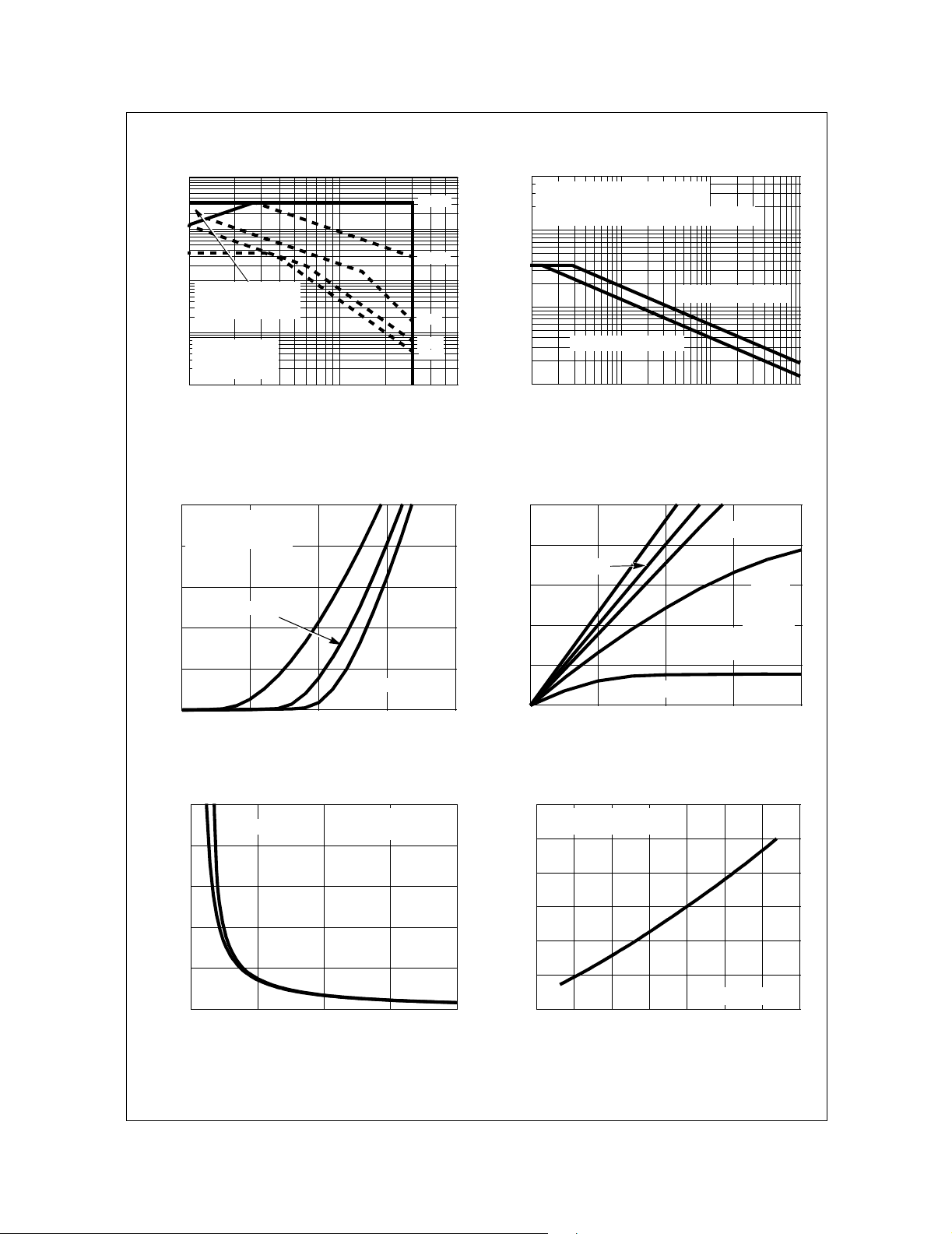
Figure 5. Forward Bias Safe Operating Area
100
PULSE DURATION = 80µs
DUTY CYCLE = 0.5% MAX
V
= 15V
DD
80
60
TJ = 25oC
40
, DRAIN CURRENT (A)
D
I
20
TJ = 175oC
0
1.5 2.0 2.5 3.0 3.5
VGS, GATE TO SOURCE VOLTAGE (V)
TJ = -55oC
10µs
100µs
1ms
10ms
DC
500
If R = 0
tAV = (L)(IAS)/(1.3*RATED BV
If R ≠ 0
= (L/R)ln[(IAS*R)/(1.3*RATED BV
t
AV
100
10
, AVALANCHE CURRENT (A)
AS
I
60
1
0.1
STARTING TJ = 150oC
1 10 100
tAV, TIME IN AVALANCHE (ms)
- VDD)
DSS
- VDD) +1]
DSS
STARTING TJ = 25oC
NOTE: Refer to Fairchild Applica ti on Note s AN75 14 and AN75 15
Figure 6. Unclamped Inductive Switching
Capability
100
VGS = 10V
80
VGS = 5V
60
40
, DRAIN CURRENT (A)
D
I
20
VGS = 2.5V
0
00.20.40.60.8
VDS, DRAIN TO SOURCE VOLTAGE (V)
VGS = 4V
PULSE DURATION = 80µs
DUTY CYCLE = 0.5% MAX
VGS = 3V
TC = 25oC
Figure 7. Transfer Characteristics Figure 8. Saturation Characteristics
14
ID = 35A
12
10
8
, DRAIN TO SOURCE
ON RESISTANCE (mΩ)
DS(ON)
r
6
ID = 1A
4
246810
V
, GATE TO SOURCE VOLTAGE (V)
GS
PULSE DURATION = 80µs
DUTY CYCLE = 0.5% MAX
Figure 9. Drain to Source On Resis tanc e vs Ga te
Voltage and Drain Current
©2008 Fairchild Semiconductor Corporation FDD8874 / FDU8874 Rev.B2
1.8
PULSE DURATION = 80µs
DUTY CYCLE = 0.5% MAX
1.6
1.4
1.2
ON RESISTANCE
1.0
0.8
NORMALIZED DRAIN TO SOURCE
0.6
-80 -40 0 40 80 120 160 200
TJ, JUNCTION TEMPERATURE (oC)
VGS = 10V, ID = 35A
Figure 10. Normalized Drain to Source On
Resistance vs Junction Temperature
Page 5
FDD8874 / FDU8874
Typical Characteristics T
1.2
1.0
0.8
NORMALIZED GATE
THRESHOLD VOLTAGE
0.6
0.4
-80 -40 0 40 80 120 160 200
TJ, JUNCTION TEMPERATURE (oC)
= 25°C unless otherwise noted
C
VGS = VDS, ID = 250µA
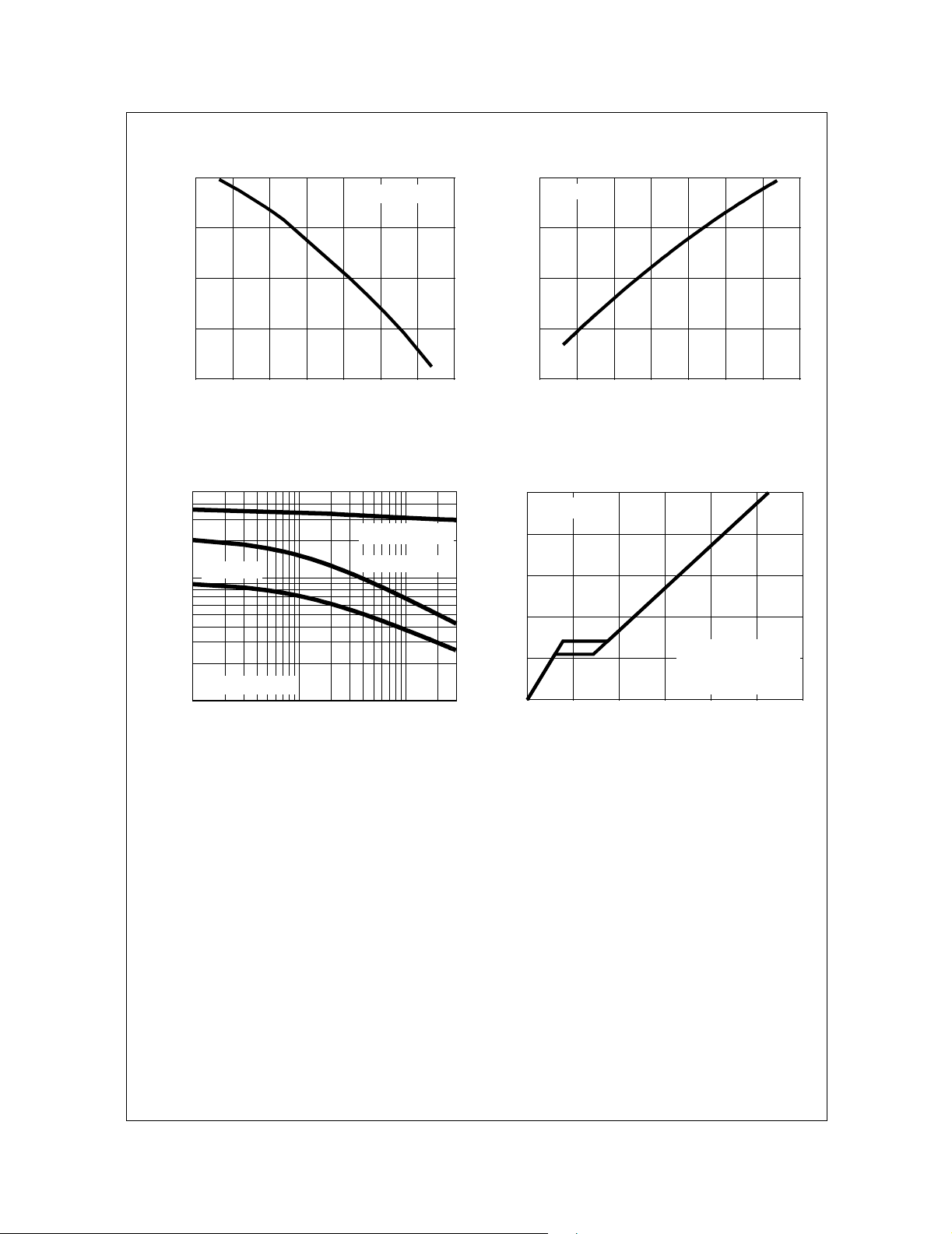
Figure 11. Normalized Gate Thresho ld Voltage vs
Junction Temperature
5000
C
= CGS + C
1000
ISS
C
C
= C
RSS
GD
OSS
≅ C
GD
+ C
DS
GD
1.10
ID = 250µA
1.05
1.00
BREAKDOWN VOLTAGE
0.95
NORMALIZED DRAIN TO SOURCE
0.90
-80 -40 0 40 80 120 160 200
TJ, JUNCTION TEMPERATURE (oC)
Figure 12. Normalized Drain to Source
Breakdown Voltage vs Junction Temperature
10
VDD = 15V
8
6
C, CAPACITANCE (pF)
V
= 0V, f = 1MHz
GS
100
0.1 1 10
VDS, DRAIN TO SOURCE VOLTAGE (V)
Figure 13. Capacitance vs Drain to Source
Voltage
4
WAVEFORMS IN
2
, GATE TO SOURCE VOLTAGE (V)
GS
V
0
30
0 102030405060
Qg, GATE CHARGE (nC)
DESCENDING ORDER:
ID = 35A
I
= 1A
D
Figure 14. Gate Charge Waveforms for Constant
Gate Current
©2008 Fairchild Semiconductor Corporation FDD8874 / FDU8874 Rev.B2
Page 6
Test Circuits and Waveforms
V
DS
L
TO OBTAIN
VARY t
P
REQUIRED PEAK I
V
GS
R
AS
G
+
V
DD
-
I
AS
DUT
t
0V
P
I
AS
0.01Ω
0
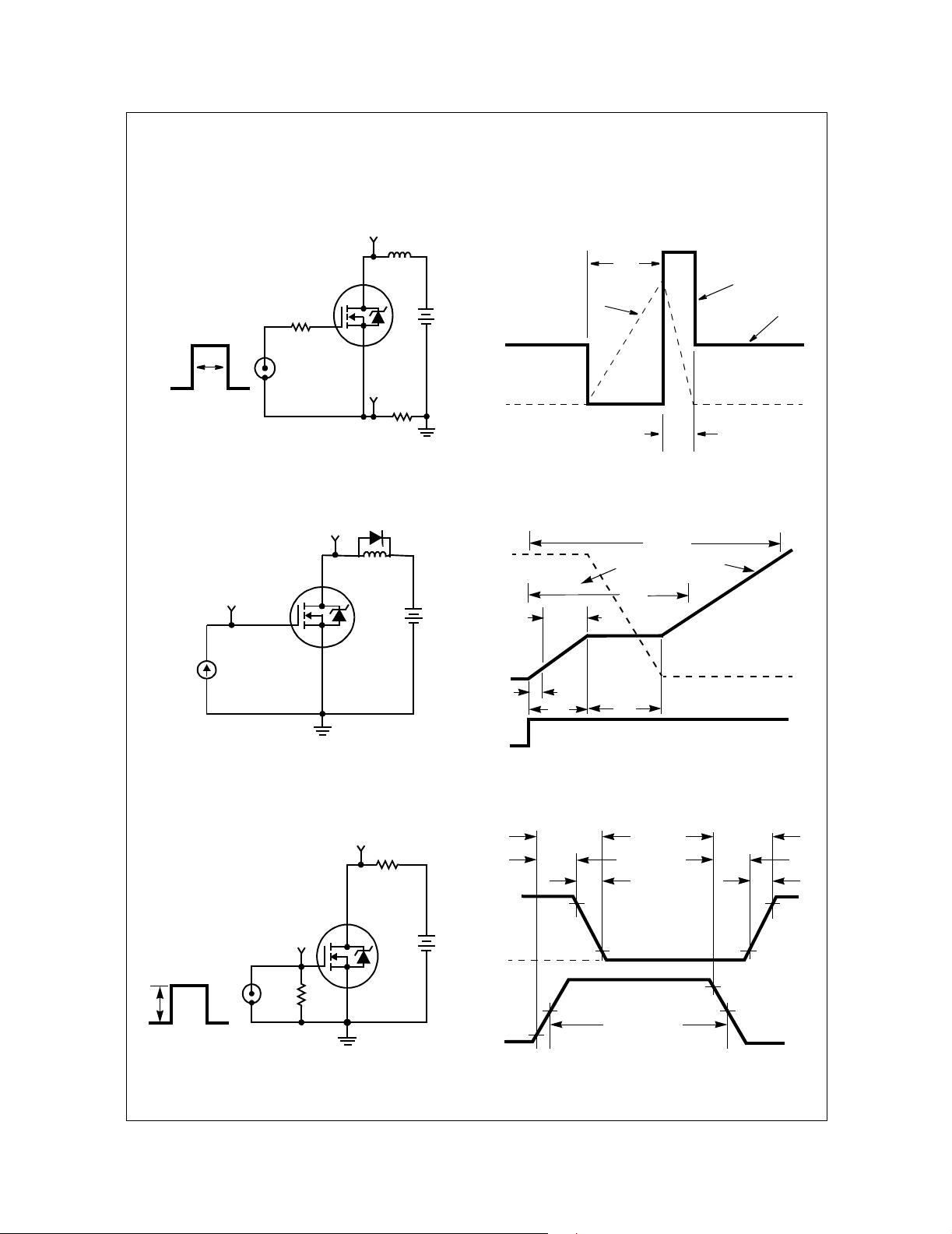
Figure 15. Unclamped Energy Test Circuit Figure 16. Unclamped Energy Waveforms
V
DS
V
DD
V
Q
I
g(REF)
L
V
GS
DUT
+
V
DD
-
V
GS
0
I
g(REF)
= 1V
Q
gs2
Q
g(TH)
Q
gs
0
Figure 17. Gate Charge Test Circuit Figure 18. Gate Charge Waveforms
BV
DSS
t
P
t
AV
Q
g(TOT)
DS
Q
g(5)
V
GS
VGS = 5V
gd
FDD8874 / FDU8874
V
DS
V
DD
V
= 10V
GS
V
DS
R
L
V
GS
R
GS
V
GS
DUT
+
V
DD
-
V
DS
0
V
GS
10%
0
t
d(ON)
90%
t
ON
50%
10%
t
r
PULSE WIDTH
t
d(OFF)
90%
t
OFF
t
f
90%
10%
50%
Figure 19. Switching Time Test Circuit Figure 20. Switching Time Waveforms
©2008 Fairchild Semiconductor Corporation FDD8874 / FDU8874 Rev.B2
Page 7
Thermal Resistance vs. Mounting Pad Area
The maximum rated junction temperature, TJM, and the
thermal resistance of the heat dissipating path determines
the maximum allowable device power dissipation, P
application. Therefore the application’s ambient
temperature, T
must be reviewed to ensure that T
Equation 1 mathematically represents the relationship and
(oC), and thermal resistance R
A
is never exceeded.
JM
DM
θJA
, in an
(oC/W)
serves as the basis for establishing the rating of the part.
P
DM
TJMTA–()
------------------- ----------=
R
θJA
(EQ. 1)
125
100
C/W)
o
(
75
θJA
R
50
R
= 33.32+ 23.84/(0.268+Area) EQ.2
θJA
R
= 33.32+ 154/(1.73+Area) EQ.3
θJA
FDD8874 / FDU8874
In using surface mount devices such as the TO-252
package, the environment in which it is applied will have a
significant influence on the part’s current and maximum
power dissipation ratings. Precise determination of P
complex and influenced by many factors:
DM
is
1. Mounting pad area onto which the device is attached and
whether there is copper on one side or both sides of t he
board.
2. The number of copper layers and the thickness of the
board.
3. The use of external heat sinks.
4. The use of thermal vias.
5. Air flow and board orientation.
6. For non steady state applications, the pulse width, the
duty cycle and the transient thermal response of the part,
the board and the environment they are in.
Fairchild provides thermal information to assist the
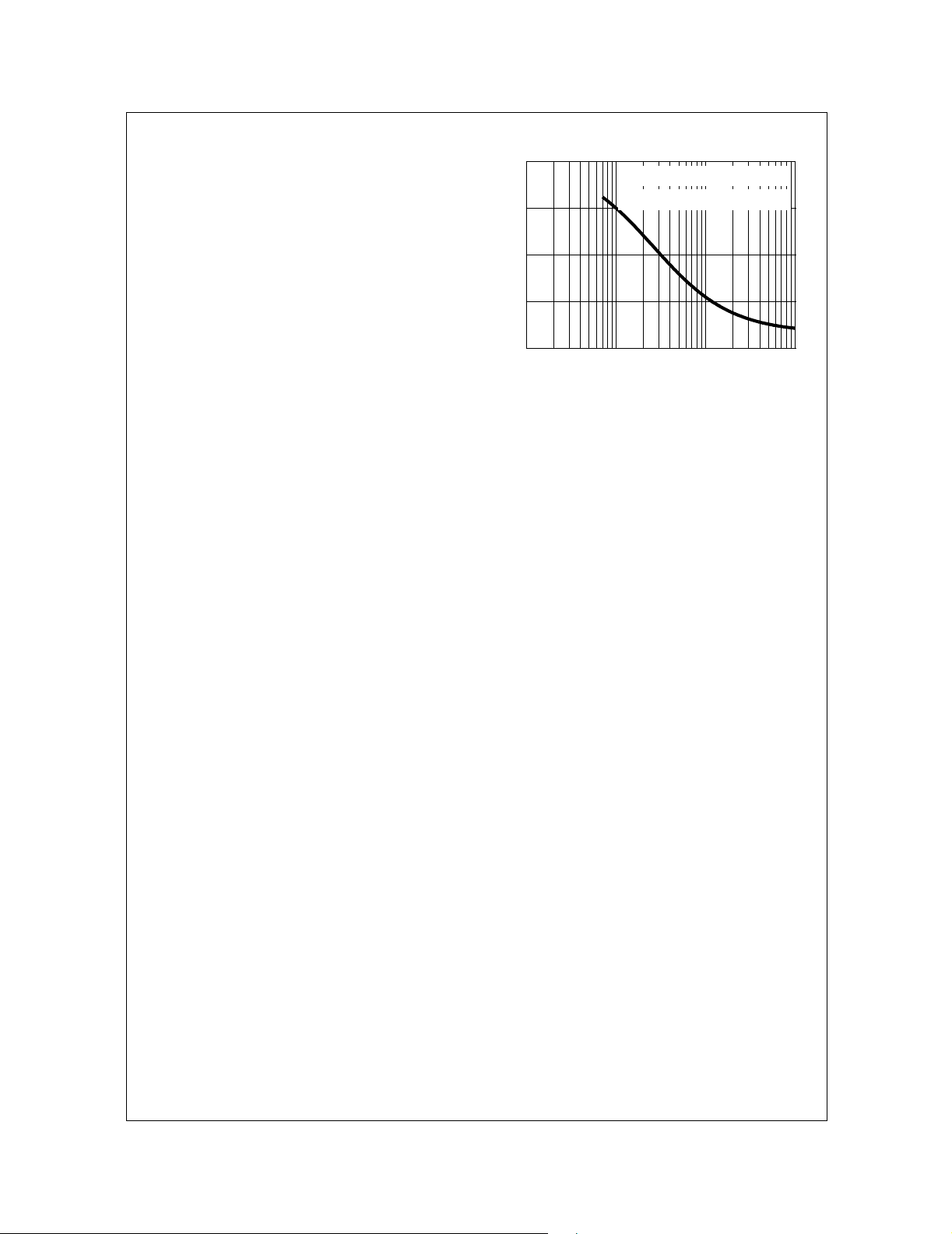
designer’s preliminary application evaluation. Figure 21
defines the R
copper (component side) area. This is for a horizontally
for the device as a function of the top
θJA
positioned FR-4 board with 1oz copper after 1000 seconds
of steady state power with no air flow. This graph provides
the necessary information for calculation of the steady state
junction temperature or power dissipation. Pulse
applications can be evaluated using the Fairchild device
Spice thermal model or manually utilizing the normalized
maximum transient thermal impedance curve.
25
0.01 0.1 1 10
(0.645) (6.45) (64.5)(0.0645)
AREA, TOP COPPER AREA in2 (cm2)
Figure 21. Thermal Resistance vs Mounting
Pad Area
Thermal resistances corresponding to other copper area s
can be obtained from Figure 21 or by calculation using
Equation 2 or 3. Equation 2 is used for copper area defined
in inches square and equation 3 is for area in centimeters
square. The area, in square inches or square centimeters is
the top copper area including the gate and source pads.
θJA
θJA
33.32
33.32
R
R
©2008 Fairchild Semiconductor Corporation FDD8874 / FDU8874 Rev.B2
23.84
-------------------------------------+=
0.268 Area+()
Area in Inches Squared
154
----------------------------------+=
1.73 Area+()
Area in Centimeters Squared
(EQ. 2)
(EQ. 3)
Page 8
PSPICE Electrical Model
.SUBCKT FDD8874 2 1 3 ; rev May 2004
Ca 12 8 2.1e-9
Cb 15 14 2.1e-9
Cin 6 8 2.7e-9
Dbody 7 5 DbodyMOD
Dbreak 5 11 DbreakMOD
Dplcap 10 5 DplcapMOD
Ebreak 11 7 17 18 33.5
Eds 14 8 5 8 1
Egs 13 8 6 8 1
Esg 6 10 6 8 1
Evthres 6 21 19 8 1
Evtemp 20 6 18 22 1
It 8 17 1
Lgate 1 9 6.5e-9
Ldrain 2 5 1.0e-9
Lsource 3 7 1.8e - 9
RLgate 1 9 65
RLdrain 2 5 10
RLsource 3 7 18
Mmed 16 6 8 8 MmedMOD
Mstro 16 6 8 8 MstroMOD
Mweak 16 21 8 8 MweakMOD
Rbreak 17 18 RbreakMOD 1
Rdrain 50 16 RdrainMOD 2e-3
Rgate 9 20 2.0
RSLC1 5 51 RSLCMOD 1e-6
RSLC2 5 50 1e3
Rsource 8 7 RsourceMOD 2e-3
Rvthres 22 8 RvthresMOD 1
Rvtemp 18 19 RvtempMOD 1
S1a 6 12 13 8 S1AMOD
S1b 13 12 13 8 S1BMOD
S2a 6 15 14 13 S2AMOD
S2b 13 15 14 13 S2BMOD
GATE
1
LGATE
RLGATE
RGATE
9
CA
ESG
+
EVTEMP
+
-
18
22
20
S1A
12
13
8
S1B
EGS EDS
-
13
6
8
10
RSLC2
6
14
13
+
+
6
8
-
-
DPLCAP
EVTHRES
+
19
8
S2A
S2B
15
CIN
CB
-
+
-
5
51
5
51
21
MSTRO
14
5
8
RSLC1
+
ESLC
50
RDRAIN
16
8
MMED
DBREAK
EBREAK
MWEAK
RSOURCE
RBREAK
17 18
IT
8
RVTHRES
FDD8874 / FDU8874
LDRAIN
RLDRAIN
11
+
17
DBODY
18
-
LSOURCE
7
RLSOURCE
RVTEMP
19
VBAT
+
22
DRAIN
2
SOURCE
3
Vbat 22 19 DC 1
ESLC 51 50 VALUE={(V(5,51)/ABS(V(5,51)))*(PWR(V(5,51)/(1e-6*500),10))}
.MODEL DbodyMOD D (IS=7E-12 IKF=10 N=1.01 RS=2.5e-3 TRS1=8e-4 TRS2=2e-7
+ CJO=1.2e-9 M=0.57 TT=1e-15 XTI=1.2)
.MODEL Dbrea kM O D D ( R S=8e-2 TRS1=1e- 3 TRS2=-8.9e-6)
.MODEL DplcapMOD D (CJO=9 .2e-10 IS=1e-30 N=10 M=0.37)
.MODEL MmedMOD NM OS (VTO =1 .8 KP= 9 IS =1 e- 3 0 N=1 0 TOX =1 L=1 u W =1 u RG=2 .0 )
.MODEL MstroMOD NMOS (VTO=2.2 KP=380 IS=1e-30 N=10 TOX=1 L=1u W=1u)
.MODEL MweakMOD NMOS (VTO=1.49 KP=0.05 IS=1e-30 N=10 T OX=1 L=1u W=1u RG=20 RS=0.1)
.MODEL RbreakMOD RES (TC1 =8.3e-4 TC2=-8e-7)
.MODEL RdrainMOD RES (TC1=6.7e-3 TC2=7e-6)
.MODEL RSLCMOD RES (TC1=1e -4 TC2=1e-6)
.MODEL RsourceMOD RES (TC1=1e-4 TC2=1e-6)
.MODEL RvthresMOD RES (TC1=-2.1e-3 TC2=-8e-6)
.MODEL RvtempMOD RES (TC1=- 1.8e-3 TC2=2e-7)
.MODEL S1AMOD VSWITCH (RON=1e-5 ROFF=0.1 VON=-4 VOFF=-3)
.MODEL S1BMOD VSWITCH (RON=1e-5 ROFF=0.1 VON=-3 VOFF=-4)
.MODEL S2AMOD VSWITCH (RON=1e-5 ROFF=0.1 VON=-2 VOFF=-0.5)
.MODEL S2BMOD VSWITCH (RON=1e-5 ROFF=0.1 VON=-0.5 VOFF=-2)
.ENDS
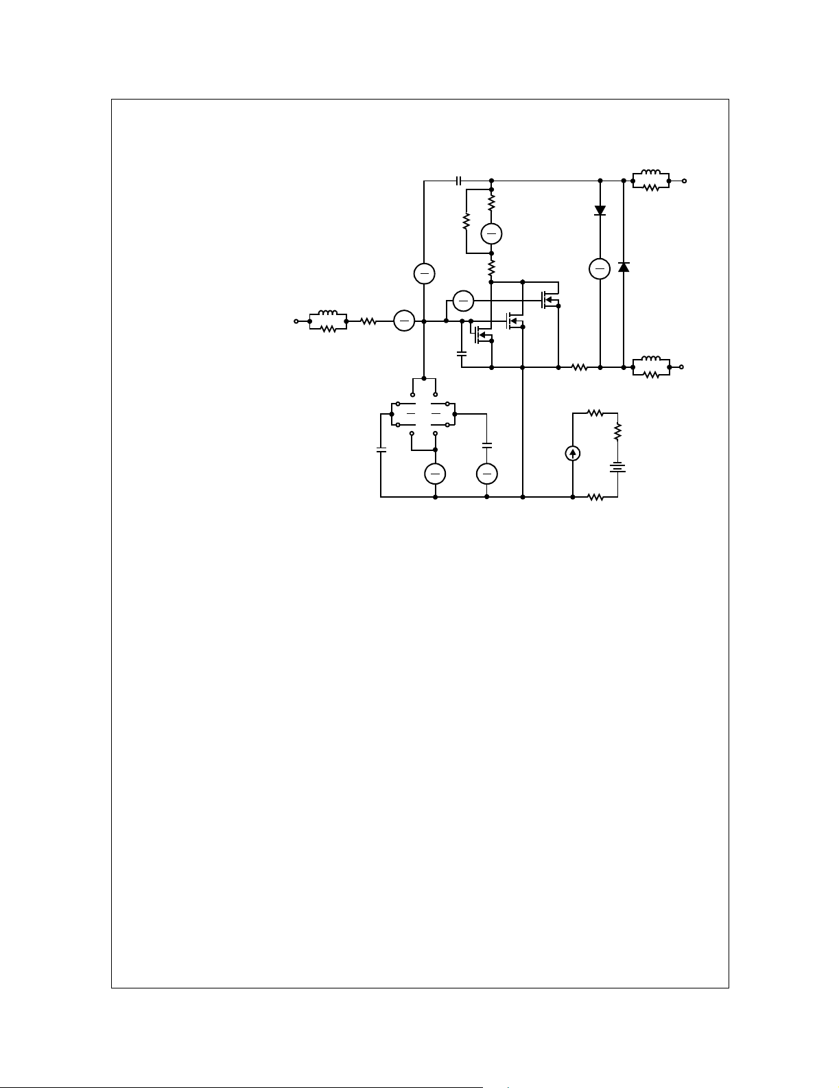
Note: For further discussio n of the PSP ICE mode l, consul t A New PSPICE Sub-Circuit for the Power MOSFET Featuring Global
Temperature Options; IEEE Power Electronics Specialist Confere nce Records, 1991, written by William J. Hepp and C. Frank
Wheatley.
©2008 Fairchild Semiconductor Corporation FDD8874 / FDU8874 Rev.B2
Page 9
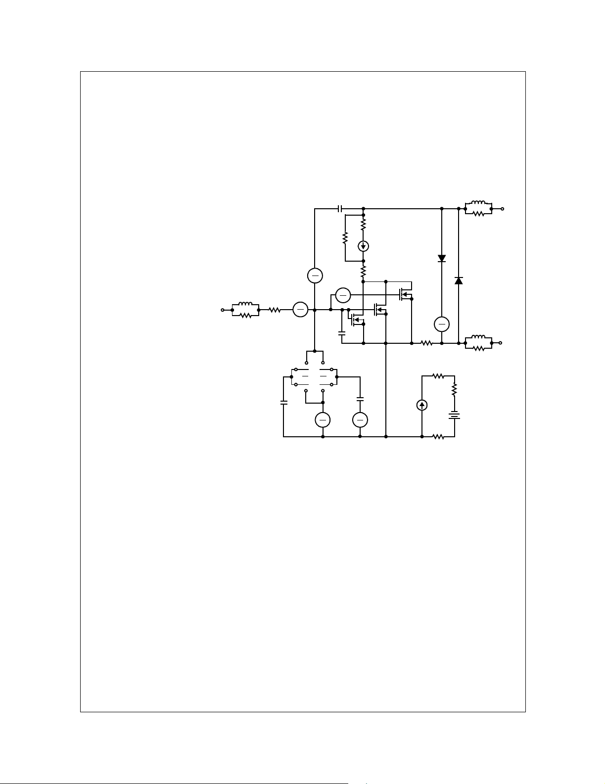
SABER Electrical Model
rev May 2004
template FDD8874 n2,n 1,n3
electrical n2,n1,n3
{
var i iscl
dp..model dbodymod = (isl=7e-12,ikf=10,nl=1.01,rs=2.5e-3,trs1=8e-4,trs2=2e-7,cjo=1.2e-9,m=0.57,tt=1e-15,xti=1.2)
dp..model dbreakmod = (rs=8e-2,trs1=1e-3,trs2=-8.9e-6)
dp..model dplcapmod = (cjo=9.2e-10,isl=10e-30,nl=10,m=0.37)
m..model mmedmod = (type=_n,vto=1.8,kp=9,is=1e-30, tox=1)
m..model mstrong mod = (type=_n,vto=2.2,k p=380,is=1e-30, tox=1 )
m..model mweakmod = (type=_n,vto=1.49,kp=0.05,is=1e-30, tox=1,rs=0.1)
sw_vcsp..model s1amod = (ron=1e-5,roff=0.1,von=-4,voff=-3)
sw_vcsp..model s1bmod = (ron=1e-5,roff=0.1,von=-3,voff=-4)
sw_vcsp..model s2amod = (ron=1e-5,roff=0.1,von=-2,voff=-0.5)
sw_vcsp..model s2bmod = (ron=1e-5,roff=0.1,von=-0.5,voff=-2)
c.ca n12 n8 = 2.1e-9
c.cb n15 n14 = 2.1e-9
c.cin n6 n8 = 2.7e-9
dp.dbody n7 n5 = model= dbodymod
dp.dbreak n5 n11 = model=dbreakmod
dp.dplcap n10 n5 = model=dplcapmod
spe.ebreak n11 n7 n17 n18 = 33.5
spe.eds n14 n8 n5 n8 = 1
spe.egs n13 n8 n6 n8 = 1
spe.esg n6 n10 n6 n8 = 1
GATE
1
LGATE
RLGATE
RGATE
9
EVTEMP
+
20
spe.evthres n6 n 21 n19 n8 = 1
spe.evtemp n20 n6 n18 n22 = 1
i.it n8 n17 = 1
l.lgate n1 n9 = 6.5e-9
l.ldrain n2 n5 = 1.0e-9
l.lsource n3 n7 = 1.8e-9
CA
S1A
12
S1B
res.rlgate n1 n9 = 65
res.rldrain n2 n5 = 10
res.rlsource n3 n7 = 18
m.mmed n16 n6 n8 n8 = model=mmedm od, l=1u, w=1u
m.mstrong n16 n6 n8 n8 = model=mstrongmod, l=1u, w=1u
m.mweak n16 n21 n8 n8 = model=mweakmod, l=1u, w=1u
res.rbreak n17 n18 = 1, tc1=8.3e-4,tc2=-8e-7
res.rdrain n50 n16 = 2e-3, tc1=6.7e-3,tc2=7e-6
res.rgate n9 n20 = 2.0
res.rslc1 n5 n51 = 1e-6, tc1=1e-4,tc2=1e-6
res.rslc2 n5 n50 = 1e3
res.rsource n8 n7 = 2e-3, tc1=1e-4,tc2=1e-6
res.rvthres n22 n8 = 1, tc1=-2.1e-3,tc2=-8e-6
res.rvtemp n18 n19 = 1, tc1=-1.8e-3,tc2=2e-7
sw_vcsp.s1a n6 n12 n13 n8 = model=s1amod
sw_vcsp.s1b n13 n12 n13 n8 = model=s1bmod
sw_vcsp.s2a n6 n15 n14 n13 = model=s2amod
sw_vcsp.s2b n13 n15 n14 n13 = model=s2bmod
ESG
18
22
DPLCAP
10
RSLC2
6
8
EVTHRES
+
+
19
8
6
-
S2A
14
13
13
8
S2B
13
+
+
6
EGS EDS
8
-
-
CIN
15
CB
-
+
-
5
MSTRO
14
5
8
RSLC1
51
ISCL
50
RDRAIN
16
21
8
MMED
DBREAK
MWEAK
EBREAK
RSOURCE
RBREAK
17 18
IT
8
RVTHRES
11
+
17
18
7
RLSOURCE
RVTEMP
19
-
+
22
LDRAIN
RLDRAIN
DBODY
LSOURCE
VBAT
DRAIN
2
SOURCE
3
FDD8874 / FDU8874
v.vbat n22 n19 = dc=1
equations {
i (n51->n50) +=iscl
iscl: v(n51,n50) = ((v(n5,n51)/(1e-9+abs(v(n5,n51))))*((abs(v(n5,n51)*1e6/500))** 10))
}
}
©2008 Fairchild Semiconductor Corporation FDD8874 / FDU8874 Rev.B2
Page 10
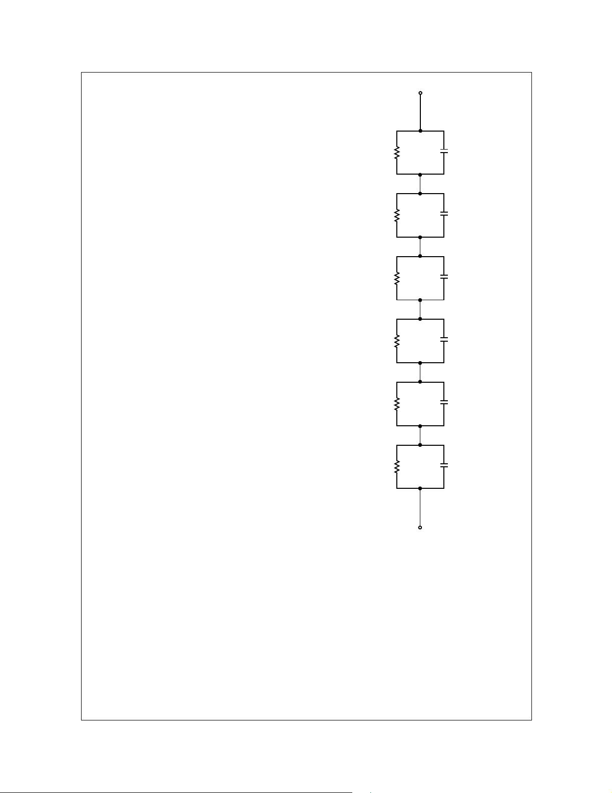
FDD8874 / FDU8874
PSPICE Thermal Model
REV 23 May 2004
FDD8874T
CTHERM1 TH 6 1.9e-3
CTHERM2 6 5 2.8e-3
CTHERM3 5 4 3.5e-3
CTHERM4 4 3 3.6e-3
CTHERM5 3 2 4.0e-3
CTHERM6 2 TL 1.6e-2
RTHERM1 TH 6 3.8e-2
RTHERM2 6 5 5.0e-2
RTHERM3 5 4 1.0e-1
RTHERM4 4 3 1.8e-1
RTHERM5 3 2 3.5e-1
RTHERM6 2 TL 3.7e-1
SABER Thermal Model
SABER thermal model FDD8874T
template thermal_model th tl
thermal_c th, tl
{
ctherm.ctherm1 t h 6 =1.9e-3
ctherm.ctherm2 6 5 =2.8e-3
ctherm.ctherm3 5 4 =3.5e-3
ctherm.ctherm4 4 3 =3.6e-3
ctherm.ctherm5 3 2 =4.0e-3
ctherm.ctherm6 2 t l =1.6e-2
rtherm.rtherm1 th 6 =3.8e-2
rtherm.rtherm2 6 5 =5.0e-2
rtherm.rtherm3 5 4 =1.0e-1
rtherm.rtherm4 4 3 =1.8e-1
rtherm.rtherm5 3 2 =3.5e-1
rtherm.rtherm6 2 tl =3.7e-1
}
RTHERM1
RTHERM2
RTHERM3
RTHERM4
RTHERM5
JUNCTION
th
CTHERM1
6
CTHERM2
5
CTHERM3
4
CTHERM4
3
CTHERM5
RTHERM6
2
CTHERM6
tl
CASE
©2008 Fairchild Semiconductor Corporation FDD8874 / FDU8874 Rev.B2
Page 11
TRADEMARKS
®
tm
tm
The following includes registered and unregistered trademarks and service marks, owned by Fairchild Semiconductor and/or its global
subsidianries, and is not intended to be an exhaustive list of all such trademarks.
®
ACEx
Build it Now™
CorePLUS™
CorePOWER™
CROSSVOLT™
CTL™
Current Transfer Logic™
EcoSPARK
®
EfficentMax™
EZSWITCH™ *
™
Fairchild
Fairchild Semiconductor
FACT Quiet Series™
FACT
FAST
FastvCore™
FlashWriter
®
®
®
®
®
*
* EZSWITCH™ and FlashWriter
FPS™
F-PFS™
®
FRFET
Global Power Resource
Green FPS™
Green FPS™ e-Series™
GTO™
IntelliMAX™
ISOPLANAR™
MegaBuck™
MICROCOUPLER™
MicroFET™
MicroPak™
MillerDrive™
MotionMax™
Motion-SPM™
OPTOLOGIC
OPTOPLANAR
®
®
are trademarks of System General Corporation, used under license by Fairchild Semiconductor.
®
®
PDP-SPM™
Power-SPM™
PowerTrench
SM
Programmable Active Droop™
QFET
®
®
QS™
Quiet Series™
RapidConfigure™
Saving our world 1mW at a time™
SmartMax™
SMART START™
®
SPM
STEALTH™
SuperFET™
SuperSOT™-3
SuperSOT™-6
SuperSOT™-8
SuperMOS™
®
The Power Franchise
TinyBoost™
TinyBuck™
TinyLogic
®
TINYOPTO™
TinyPower™
TinyPWM™
TinyWire™
µSerDes™
®
UHC
Ultra FRFET™
UniFET™
VCX™
VisualMax™
DISCLAIMER
FAIRCHILD SEMICONDUCTOR RESERVES THE RIGHT TO MAKE CHANGES WITHOUT FURTHER NOTICE TO ANY PRODUCTS
HEREIN TO IMPROVE RELIABILITY, FUNCTION, OR DESIGN. FAIRCHILD DOES NOT ASSUME ANY LIABILITY ARISING OUT OF THE
APPLICATION OR USE OF ANY PRODUCT OR CIRCUIT DESCRIBED HEREIN; NEITHER DOES IT CONVEY ANY LICENSE UNDER
ITS PATENT RIGHTS, NOR THE RIGHTS OF OTHERS. THESE SPECIFICATIONS DO NOT EXPAND THE TERMS OF FAIRCHILD’S
WORLDWIDE TERMS AND CONDITIONS, SPECIFICALLY THE WARRANTY THEREIN, WHICH COVERS THESE PRODUCTS.
®
LIFE SUPPORT POLICY
FAIRCHILD’S PRODUCTS ARE NOT AUTHORIZED FOR USE AS CRITICAL COMPONENTS IN LIFE SUPPORT DEVICES OR
SYSTEMS WITHOUT THE EXPRESS WRITTEN APPROVAL OF FAIRCHILD SEMICONDUCTOR CORPORATION.
As used herein:
1. Life support devices or systems are devices or systems which,
(a) are intended for surgical implant into the body or (b)
support or sustain life, and (c) whose failure to perform when
properly used in accordance with instructions for use provided
2. A critical component in any component of a life support,
device, or system whose failure to perform can be reasonably
expected to cause the failure of the life support device or
system, or to affect its safety or effectiveness.
in the labeling, can be reasonably expected to result in a
significant injury of the user.
PRODUCT STATUS DEFINITIONS
Definition of Terms
Datasheet Identification Product Status Definition
Advance Information Formative or In Design
This datasheet contains the design specifications for product development.
Specifications may change in any manner without notice.
This datasheet contains preliminary data; supplementary data will be pub-
Preliminary First Production
lished at a later date. Fairchild Semiconductor reserves the right to make
changes at any time without notice to improve design.
No Identification Needed Full Production
Obsolete Not In Production
@2008 Fairchild Semiconductor Corporation
This datasheet contains final specifications. Fairchild Semiconductor reserves
the right to make changes at any time without notice to improve the design.
This datasheet contains specifications on a product that is discontinued by
Fairchild Semiconductor. The datasheet is for reference information only.
FDD8874 / FDU8874 Rev. B2
Rev. I34
 Loading...