

Page 1

FDC37N972
ADVANCE INFORMATION
Ad vanced Notebook I/O Controller with Enhanced
Keyboard Control and System Management
FEATURES
!" 3.3V Operation With 5V Tolerant Buffers
!" ACPI 1.0 and PC99 Compliant
!" Three Power Planes
!" ACPI Embedded Controller Interface
!" Low Standby Current in Sleep Mode
!" Configuration Register Set Compatible With
ISA Plug-and-Play Standard (Version 1.0a)
!" Serial IRQ Interface Compatible With
Serialized IRQ Support for PCI Systems
!" Floppy Disk Interface on Parallel Port
!" 8051 Controller uses Parallel Port to
Reprogram the Flash ROM
!" Advanced Infrared Communications
Controller (IrCC 2.0)
- IrDA V1.1 (4Mbps), HPSIR, ASKIR,
Consumer IR Support
- Two IR Ports
- Relocatable Base I/O Address
!" 512k Byte Flash ROM Interface
- 8051/Host CPU Multiplexed Interface
- Sixteen 32K Pages - 8051 Keyboard
BIOS
- Eight 64K Pages - Host System BIOS
- Embedded Controller uses Parallel Port
to Reprogram Flash ROM
!" ISA Host Interface With Clock Run Support
and ACPI SCI Interface
- 16 Bit Address Qualification
- 8 Bit Data Bus
- Zero Wait-State I/O Register Access
- Shadowed Write Only registers
- IOCHRDY for ECP, IRCC 2.0 and Flash
Cycles
- 15 Direct IRQs Including nSMI
- Four 8 Bit DMA Channels
- XNOR Test Chain
!"High-Performance Embedded 8051
Keyboard and System Controller
- Provides System Power Management
- System Watch Dog Timer (WDT)
- 8042 Style Host Interface
- Asynchronous Access to Two Data
Registers and One Status Register
- Supports Interrupt and Polling Access
- 2K Internal ROM, nEA Pin Select
- 32K Bank Switchable External Flash
ROM Interface
- 256 Bytes Data RAM
- On-Chip Control Registers Available via
MOVX External Data Access Commands
- Access to RTC and CMOS Registers
- Up to 16x8 Keyboard Scan Matrix
- Three 16 Bit Timer/Counters
- Integrated TX/RX Serial Interface
- Eleven 8051 Interrupt Sources
- Thirty-Two 8 Bit, Host/8051 Mailbox
Registers
- Thirty Maskable Hardware Wake-Up
Events Supported
- Fast GATEA20
- Fast CPU_RESET
- Multiple Clock Sources and Frequencies
- IDLE and SLEEP Modes
- Fail-Safe Ring Oscillator
!"Real Time Clock
- MC146818 and DS1287 Compatible
- 256 Bytes of Battery Backed CMOS in
Two 128-Byte Banks
- 128 Bytes of CMOS RAM Lockable in
4x32 Byte Blocks
- 12 and 24 Hour Time Format
- Binary and BCD Format
Page 2

- <2!A Standby Current (typ)
!"
Two 8584-Style ACCESS.bus Controllers
!"
Four independent Hardware Driven PS/2
Ports
!"
General Purpose I/O
- 22 I/O Pins
- 12 Out Pins
- Eight In Pins
!"
Two Programmable Pulse-Width Modulator
Outputs
- Independent Clock Rates
- 6 Bit Duty Cycle Granularity
- VCC1 and VCC2 operation mode
!"
Intelligent Auto Power Management
!"
2.88MB Super I/O Floppy Disk Controller
- Relocatable to 480 Different Base I/O
Addresses
- 15 IRQ Options
- Four DMA Options
- Open-Drain/Push-Pull Configurable
Output Drivers
- Licensed CMOS 765B Floppy Disk
Controller
- Advanced Digital Data Separator
- Software and Register Compatible With
SMSC's Proprietary 82077AA Compatible
Core
- Low Power CMOS Design with
Sophisticated Power Control Circuitry
(PCC) Including Multiple Powerdown
Modes for Reduced Power Consumption
- Supports Two Floppy Drives on the FDD
Interface and Two Floppy Drives on the
Parallel Port Interface
- 12 mA FDD Interface Cable Drivers With
Schmitt Trigger Inputs
!"
Licensed CMOS 765B Floppy Disk Controller
Core
- Supports Vertical Recording Format
- 16-Byte Data FIFO
- 100% IBM Compatibility
- Detects All Overrun and Underrun
Conditions
- 12 mA Drivers and Schmitt Trigger Inputs
- DMA Enable Logic
- Data Rate and Drive Control Registers
!"
Enhanced Digital Data Separator
- Low Cost Implementation
- No Filter Components Required
- 2 Mbps, 1 Mbps, 500 Kbps, 300 Kbps,
250 Kbps Data Rates
- Programmable Precompensation Modes
!"
Multi-Mode Parallel Port with ChiProtect
- Standard Mode IBM PC/XT, PC/AT, and
PS/2 Compatible Bi-directional Parallel
Port
- Enhanced Parallel Port EPP 1.7 and EPP
1.9 Compatible (IEEE 1284 Compliant)
IEEE 1284 Compliant Enhanced
Capabilities Port (ECP)
- ChiProtect Circuitry to Prevent Printer
Power-On Damage
- Relocatable to 480 Different Base I/O
Addresses
- 15 IRQ Options
- 4 DMA Options
- Microsoft and HP compatible High Speed
Mode
- 12 mA Output Drivers
!"
Serial Port
- High-Speed NS16550A-Compatible
UART with 16-Byte Send/Receive FIFOs
- Programmable Baud Rate Generator
Modem Control Circuitry Including 230k
and 460k Baud
- Relocatable to 480 Different Base I/O
Addresses
- 15 IRQ Options
!"
208 Pin TQFP Package Options
!"
208 Pin FBGA Package Options
2
Page 3

GENERAL DESCRIPTION
The FDC37N972 is a 208-pin 3.3V ISA Host
ACPI 1.0 and PC98 (/PC99)-compliant Ultra I/O
Controller with Fast Infrared for mobile
applications.
The FDC37N972 incorporates a highperformance 8051-based keyboard controller; a
512k byte Flash ROM interface; four PS/2 ports;
a real-time clock; SMSC's true CMOS 765B
floppy disk controller with advanced digital data
separator and 16-byte data FIFO; an
NS16C550A-compatible UART, SMSC’s
advanced Infrared Communications Controller
(IrCC 2.0) with a UART and a Synchronous
Communications Engine to provide IrDA v1.1
(Fast IR) capabilities; one Multi-Mode parallel
port with ChiProtect circuitry plus EPP and ECP
support; two 8584-style Access Bus controllers;
a Serial IRQ peripheral agent interface; an ACPI
Embedded Controller Interface; General
Purpose I/O pins; two independently
programmable pulse width modulators; twofloppy direct drive support; and maskable
hardware wake-up events.
The true CMOS 765B core provides 100%
compatibility with IBM PC/XT and PC/AT
architectures in addition to providing data
overflow and underflow protection. The SMSC
advanced digital data separator incorporates
SMSC's patented data separator technology,
allowing for ease of testing and use.
The parallel port is compatible with IBM PC/AT
architecture, as well as EPP and ECP. The
8051 controller can also take control of the
parallel port interface to provide remote
diagnostics or “Flashing” of the Flash memory.
The FDC37N972 has three separate power
planes to provide “instant on” and system power
management functions. Additionally, the
FDC37N972 incorporates sophisticated power
control circuitry (PCC). The PCC supports
multiple low power down modes. Wake-up
events and ACPI-related functions are supported
through the SCI Interface.
The FDC37N972’s configuration register set is
compatible with the ISA Plug-and-Play Standard
(Version 1.0a) and provides the functionality to
support Windows '95. Through internal
configuration registers, each of the
FDC37N972's logical device's I/O address, DMA
channel and IRQ channel may be programmed.
There are 480 I/O address location options, 15
IRQ options, and four DMA channel options for
each logical device.
The FDC37N972 does not require any external
filter components and is, therefore, easy to use
and offers lower system cost and reduced board
area. The FDC37N972 is software and register
compatible with SMSC's proprietary 82077AA
core.
3
Page 4

TABLE OF CONTENTS
FEATURES.......................................................................................................................................1
GENERAL DESCRIPTION................................................................................................................3
PIN CONFIGURATION......................................................................................................................9
DESCRIPTION OF PIN FUNCTIONS..............................................................................................11
FUNCTIONAL DESCRIPTION.........................................................................................................28
FLOPPY DISK CONTROLLER........................................................................................................30
FDC INTERNAL REGISTERS......................................................................................................30
STATUS REGISTER ENCODING................................................................................................44
FDC RESET.................................................................................................................................46
FDC MODES OF OPERATION....................................................................................................47
DMA TRANSFERS.......................................................................................................................47
CONTROLLER PHASES.................................................................................................................47
FDC INSTRUCTION SET.............................................................................................................53
FDC DATA TRANSFER COMMANDS..........................................................................................64
ACPI EMBEDDED CONTROLLER..................................................................................................82
ECI CONFIGURATION REGISTERS............................................................................................83
SERIAL PORT (UART)....................................................................................................................86
FIFO INTERRUPT MODE OPERATION.......................................................................................97
FIFO POLLED MODE OPERATION.............................................................................................97
INFRARED COMMUNICATIONS CONTROLLER (IRCC 2.0).........................................................102
OVERVIEW................................................................................................................................103
IRRX/IRTX PIN ENABLE.............................................................................................................104
IR REGISTERS - LOGICAL DEVICE 5........................................................................................104
IR DMA CHANNELS...................................................................................................................105
S.......................................................................................................................................105
IR IRQ
IR HALF DUPLEX TIMEOUT.......................................................................................................106
IRTX OUTPUT PINS DEFAULT...................................................................................................106
PARALLEL PORT.......................................................................................................................106
THE PARALLEL PORT PHYSICAL INTERFACE (PPPI)..............................................................128
PARALLEL PORT FDC INTERFACE...........................................................................................129
AUTO POWER MANAGEMENT.....................................................................................................131
SYSTEM POWER MANAGEMENT.............................................................................................131
DSR FROM POWERDOWN.......................................................................................................132
WAKE UP FROM AUTO POWERDOWN....................................................................................132
REGISTER BEHAVIOR...............................................................................................................132
PIN BEHAVIOR...........................................................................................................................132
SYSTEM INTERFACE PINS........................................................................................................133
4
Page 5

FDD INTERFACE PINS...............................................................................................................134
UART POWER MANAGEMENT..................................................................................................135
PARALLEL PORT POWER MANAGEMENT................................................................................135
8051 EMBEDDED CONTROLLER .................................................................................................136
8051 FUNCTIONAL OVERVIEW.................................................................................................136
POWERING UP OR RESETTING THE 8051...............................................................................137
CPU RESET SEQUENCE...........................................................................................................140
8051 CLOCK CONTROLS ..........................................................................................................142
8051 RING OSCILLATOR FAIL-SAFE CONTROLS ....................................................................144
8051 MEMORY MAP...................................................................................................................145
FLASH ROM INTERFACE...........................................................................................................152
8051 CONTROL REGISTERS.....................................................................................................153
8051 CONFIGURATION/CONTROL MEMORY MAPPED REGISTERS .........................................162
8051 INTERRUPTS.....................................................................................................................165
WATCH DOG TIMER.....................................................................................................................183
WDT OPERATION......................................................................................................................183
WDT ACTION.............................................................................................................................183
WDT ACTIVATION .....................................................................................................................183
WDT RESET MECHANISM .........................................................................................................183
WDT MEMORY MAPPED REGISTERS ......................................................................................184
SHARED FLASH INTERFACE.......................................................................................................185
FLASH INTERFACE DIAGRAM...................................................................................................185
SYSTEM MEMORY MAP............................................................................................................186
KEYBOARD BIOS (KMEM).........................................................................................................187
SYSTEM BIOS (HMEM)..............................................................................................................189
HOST FLASH ACCESS ..............................................................................................................189
IDLE MODE................................................................................................................................195
SLEEP MODE.............................................................................................................................197
WAKE-UP EVENTS....................................................................................................................201
8042 STYLE HOST INTERFACE.................................................................................................204
KEYBOARD DATA WRITE..........................................................................................................204
8051- TO- HOST KEYBOARD COMMUNICATION......................................................................205
HOST-TO 8051 KEYBOARD COMMUNICATION........................................................................206
GATEA20 HARDWARE SPEED-UP............................................................................................208
SMSC PS/2 LOGIC OVERVIEW.................................................................................................217
SMSC PS/2 MEMORY MAPPED CONTROL REGISTERS ..........................................................218
DEVIL LOGIC OVERVIEW..........................................................................................................225
THE DEVIL PS/2 LOGIC COMMANDS........................................................................................225
DEVIL PS/2 MEMORY MAPPED CONTROL REGISTERS..........................................................227
5
Page 6

ACCESS.BUS................................................................................................................................233
BACKGROUND ..........................................................................................................................233
REGISTER DESCRIPTION.........................................................................................................234
ACCESS.BUS INTERFACE DESCRIPTION................................................................................238
MEMORY MAPPED CONTROL REGISTERS..............................................................................239
SECOND I2C BUS INTERFACE .....................................................................................................241
MEMORY MAPPED CONTROL REGISTERS..............................................................................241
I2C CLOCK DIVIDER BIT............................................................................................................243
OVERVIEW................................................................................................................................244
MAILBOX REGISTERS INTERFACE BASE ADDRESS...............................................................246
MAILBOX REGISTERS...............................................................................................................247
THE SYSTEM/8051 INTERFACE REGISTERS`..........................................................................247
LED CONTROLS........................................................................................................................249
PULSE WIDTH MODULATORS..................................................................................................250
OPERATION REGISTERS..........................................................................................................257
GENERAL PURPOSE I/O (GPIO)..................................................................................................260
OVERVIEW................................................................................................................................266
MULTIPLEXING_1 REGISTER ...................................................................................................266
MULTIPLEXING_2 REGISTER ...................................................................................................270
MULTIPLEXING_3 REGISTER ...................................................................................................272
ACPI PM1 BLOCK.........................................................................................................................276
ACPI PM1 BLOCK OVERVIEW...................................................................................................276
ACPI PM1 BLOCK SCI EVENT-GENERATING FUNCTIONS ......................................................276
ACPI PM1 BLOCK BASE ADDRESS ...........................................................................................277
ACPI PM1 BLOCK ......................................................................................................................278
REGISTERS...............................................................................................................................278
REAL TIME CLOCK.......................................................................................................................283
GENERAL DESCRIPTION..........................................................................................................283
CONFIGURATION REGISTERS.................................................................................................283
ISA HOST I/O INTERFACE .........................................................................................................284
INTERNAL REGISTERS.............................................................................................................285
TIME CALENDAR AND ALARM ..................................................................................................286
UPDATE CYCLE .........................................................................................................................287
CONTROL AND STATUS REGISTERS.......................................................................................288
INTERRUPTS.............................................................................................................................292
FREQUENCY DIVIDER...............................................................................................................292
32KHZ CLOCK INPUT.................................................................................................................295
POWER MANAGEMENT ............................................................................................................295
6
Page 7

PCI CLOCK RUN SUPPORT..........................................................................................................295
OVERVIEW................................................................................................................................295
SERIAL INTERRUPTS...................................................................................................................298
SERIRQ MODE BIT FUNCTION .................................................................................................299
FDC37N972 CONFIGURATION ....................................................................................................303
OVERVIEW................................................................................................................................303
CONFIGURATION REGISTER ACCESS.....................................................................................303
CHIP LEVEL (GLOBAL) CONTROL/CONFIGURATION REGISTERS [0X00-0X2F].....................308
LOGICAL DEVICE CONFIGURATION/CONTROL REGISTERS [0X30-0XFF].............................311
I/O BASE ADDRESS CONFIGURATION REGISTER DESCRIPTION ..........................................313
INTERRUPT SELECT CONFIGURATION REGISTER DESCRIPTION........................................315
DMA CHANNEL SELECT CONFIGURATION REGISTER DESCRIPTION...................................316
IRQ AND DMA ENABLE AND DISABLE......................................................................................317
SMSC DEFINED LOGICAL DEVICE CONFIGURATION REGISTERS.........................................318
ELECTRICAL SPECIFICATIONS...................................................................................................327
MAXIMUM GUARANTEED RATINGS*........................................................................................327
DC SPECIFICATIONS ................................................................................................................328
AC SPECIFICATIONS.................................................................................................................332
TIMING DIAGRAMS ......................................................................................................................333
LOAD CAPACITANCE ................................................................................................................333
FAST GATEA20 IOW TIMING.....................................................................................................334
ISA IO WRITE ............................................................................................................................335
ISA IO READ CYCLE..................................................................................................................336
DMA TIMING (BURST TRANSFER MODE) .................................................................................340
FLOPPY DISK DRIVE TIMING (AT MODE).................................................................................341
SERIAL PORT TIMING...............................................................................................................342
PARALLEL PORT TIMING..........................................................................................................343
EPP 1.9 DATA OR ADDRESS WRITE CYCLE............................................................................344
EPP 1.9 DATA OR ADDRESS READ CYCLE ..............................................................................346
EPP 1.7 DATA OR ADDRESS WRITE CYCLE............................................................................348
EPP 1.7 DATA OR ADDRESS READ CYCLE ..............................................................................350
ECP PARALLEL PORT TIMING..................................................................................................351
ACCESS.BUS TIMING................................................................................................................355
HOST FLASH READ TIMING......................................................................................................356
HOST FLASH READ/WRITE.......................................................................................................358
ZERO WAIT STATE (NOWS) TIMING........................................................................................360
FLASH PROGRAM FETCH TIMING ............................................................................................361
8051 FLASH READ TIMING ........................................................................................................362
8051 FLASH WRITE TIMING......................................................................................................363
7
Page 8

EPP 1.7 DATA OR ADDRESS READ CYCLE.............................................................................353
ECP PARALLEL PORT TIMING..................................................................................................354
ACCESS.BUS TIMING..................................................................................................................358
HOST FLASH READ TIMING......................................................................................................359
HOST FLASH READ/WRITE.......................................................................................................361
ZERO WAIT STATE (NOWS) TIMING.......................................................................................363
FLASH PROGRAM FETCH TIMING...........................................................................................364
8051 FLASH READ TIMING........................................................................................................365
8051 FLASH WRITE TIMING......................................................................................................366
PS/2 CHANNEL RECEIVE TIMING DIAGRAM ........................................................................367
PS/2 CHANNEL TRANSMIT TIMING DIAGRAM.....................................................................369
PS/2 CHANNEL “BIT-BANG” TIMING......................................................................................371
IN CIRCUIT TEST (ICT)................................................................................................................373
APPENDIX A...................................................................................................................................377
HIGH-PERFORMANCE 8051 CYCLE TIMING AND INSTRUCTION SET.............................377
APPENDIX B...................................................................................................................................382
HIGH PERFORMANCE 8051 EXTENDED INTERRUPT UNIT................................................382
8
Page 9
IN5
OUT5
OUT6
DRVDEN0
DRVDEN1
nMTR0
nDS0
nDIR
nSTEP
nWDATA
nWGATE
nHDSEL
nINDEX
nTRK0
nRDATA
nDSKCHG
KSO13
KSO12
KSO11
KSO10
KSO9
KSO8
KSO7
VCC1
KSO6
KSO5
KSO4
KSO3
KSO2
KSO1
KSO0
IN6
IN7
VCC0
IN1
IN2
IN3
IN4
GPIO10
GPIO11
GPIO12
IN0
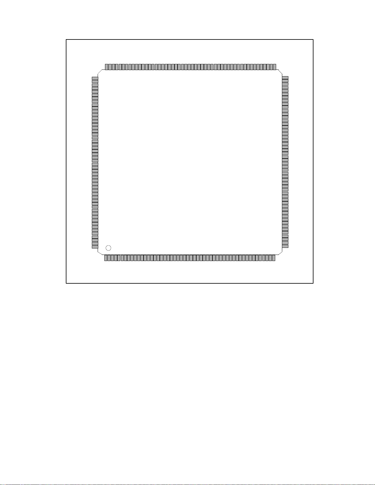
PIN CONFIGURATION
GPIO15
GPIO14
GPIO8
GPIO9
VCC1
FA18
nDCD
nRI
nDTR
nCTS
nDSR
TXD
nRTS
VSS
nERROR
nALF
RXD
nSTROBE
PD1
PD0
nSLCTIN
nINIT
PD5
PD4
PD3
PD2
VCC2
PD7
PD6
BUSY
nACK
VCC1_PWRGD
PWRGD
PE
nPWR_LED
SLCT
32kHz_OUT
24MHz_OUT
nEC_SCI
VSS
XOSEL
XTAL1
XTAL2
AGND
FAD0
FAD1
FAD2
FAD3
FAD4
FAD5
VSS
FAD6
FAD7
FA8
FA9
FA10
FA11
FA12
FA13
VCC1
FA14
FA15
FA16
FA17
FALE
nFRD
nFWR
nFCS
GPIO1
GPIO2
GPIO3
GPIO4
GPIO5
GPIO6
GPIO7
VSS
nEA
MODE
AB1_DATA
AB1_CLK
nBAT_LED
nFDD_LED
OUT11
OUT10
OUT9
OUT8
OUT7
GPIO16
VCC2
GPIO17
GPIO18
GPIO19
155
153
154
156
157
158
159
160
161
162
163
164
165
166
167
168
169
170
171
172
173
174
175
176
177
178
179
180
181
182
183
184
185
186
187
188
189
190
191
192
193
194
195
196
197
198
199
200
201
202
203
204
205
206
207
208
123467891011121314151617181920222324252627282930313233343536373839404142434445464748495051
147
148
149
150
151
152
5
141
142
143
144
145
146
FDC37N972
208 PIN TQFP
135
136
137
138
139
140
21
129
130
131
132
133
134
123
124
125
126
127
128
117
118
119
120
121
122
111
112
113
114
115
116
105
106
107
108
109
110
VCC2
104
CLOCKI
103
nRESET_OUT
102
SER_IRQ
101
nCLKRUN
100
PCI_CLK
99
nMEMWR
98
nMEMRD
97
nROMCS
96
IOCHRDY
95
TC
94
DRQ1
93
nDACK1
92
DRQ0
91
nDACK0
90
VSS
89
SD7
88
SD6
87
SD5
86
SD4
85
SD3
84
VCC2
83
SD2
82
SD1
81
SD0
80
AEN
79
nIOW
78
nIOR
77
nNOWS
76
OUT4
75
OUT3
74
VSS
73
OUT2
72
nIRQ8
71
OUT0
70
SA15
69
SA14
68
SA13
67
SA12
66
SA11
65
SA10
64
SA9
63
SA8
62
SA7
61
SA6
60
SA5
59
SA4
58
SA3
57
SA2
56
SA1
55
SA0
54
EMDAT
53
52
VSS
VSS
nWRTPRT
FPD
IRTX
IRRX
KSI7
KSI6
KSI5
KSI4
KSI3
KSI2
KSI1
GPIO20
GPIO21
KSI0
VSS
IMCLK
IMDAT
EMCLK
KCLK
KDAT
FIGURE 1 - FDC37N972 PIN CONFIGURATION
For FBGA BALL PAD Configuration refer to FIGURE 81 on Page 372.
9
Page 10
nRESET_OUT
nIOR
nIOW
nMEMRD
nMEMWR
nROMCS
SA[0:15]
SD[0:7]
DRQ[0:1]
DRQ[2:3]*
nDACK[0:1]
nDACK[2:3]*
nNOWS
IOCHRDY
nIRQ8*
nSMI*
SER_IRQ
nCLKRUN
PCI_CLK
MODE
VCC1_PWRGD
PWRGD
32KHz_OUT
24MHz_OUT
CLOCKI
(14.318 MHz)
XOSEL
XTAL2
XTAL1
VCC0
AGND
DIGITAL DATA
SEPARATOR
WITH WRITE
VCC1(3)
VCC2(4)
VSS(9)
SYSTEM
RESET
AEN
HOST
CPU
TC
INTERFACE
INTERRUPTS
nEA
CONTROL
INPUTS
PLL CLOCK
GENERATOR
RTC
2 x 128 BYTE
BANKS OF
CMOS RAM
BANK
1
nEC_SCI
BANK
2
PRECOMPENSATION
MDATA
MCLOCK
SMSC
PROPRIETARY
82077 COMPATIBLE
VERTICAL FLOPPY DISK
CONTROLLER CORE
CONFIGURATION REGISTERS
CONTROL, ADDRESS, DATA
ACPI
EMBEDDED
CONTROLLER
PM1
BLOCK
256B Direct
w/ FAIL SAFE
WDT
* -- ALTERNATE FUNCITON
RDATA
8051
Oscillator
nWDATA
nRDATA
RCLOCK
nDSKCHG, nWRTPRT,
nTRK0, nINDEX, FPD, nTRK0
nWGATE, nHDSEL, nDIR,
nSTEP, nDS0, nDS1*, nMTR0,
nMTR1*, DRVDEN0, DRVDEN1*,
FPD
POWER
MANAGEMENT
MAILBOX
REGISTERS
8051
SUB-BLOCK
EXTERNAL
RAM
Ring
CONTROL
REGISTERS
256B
EXTERNAL
8051 RAM
16C550
COMPATIBLE
SERIAL PORT 1
INFRARED
MULTI-MODE
PARALLEL
PORT / FDC
MUX
GENERAL
PURPOSE I/O
INTERFACE
LED
DRIVER
16 x 8
KEYBOARD
INTERFACE
PS/2
PORTS
ACCESS
BUS
ACCESS
BUS2
PWM
FLASH
VCC2 POWERED
VCC1 POWERED
INTERFACE
TXD, nRTS, nDTR
RXD, nCTS, nDSR, nDCD
nRI
IRRX*
IRRX2
IRMODE / IRRX3A, IRMODE / IRRX3B
IRTX*
IRTX2
PD[0:7]
BUSY, SLCT, PE, nERROR, nACK
nSLCTIN, nINIT, nALF, nSTROBE
IN0-7
IN
OUT0-11
OUT
GPIO 16-21
I/O
GPIO 0-15
I/O
nBAT_LED, nPWR_LED, nFDD_LED
KSI[0:7]
KS0[0:13], KS0[14:15]*
KCLK, EMCLK, IMCLK, PS2CLK
KDAT, EMDAT, IMDAT, PS2DAT
AB_DATA, AB_CLK
AB2_DATA *, AB2_CLK *
PWM0*, PWM1*
FAD[0:7]
FA[8:18], nFRD, nFWR, FALE
nFCS
FDC37N97x
(TIKKI)
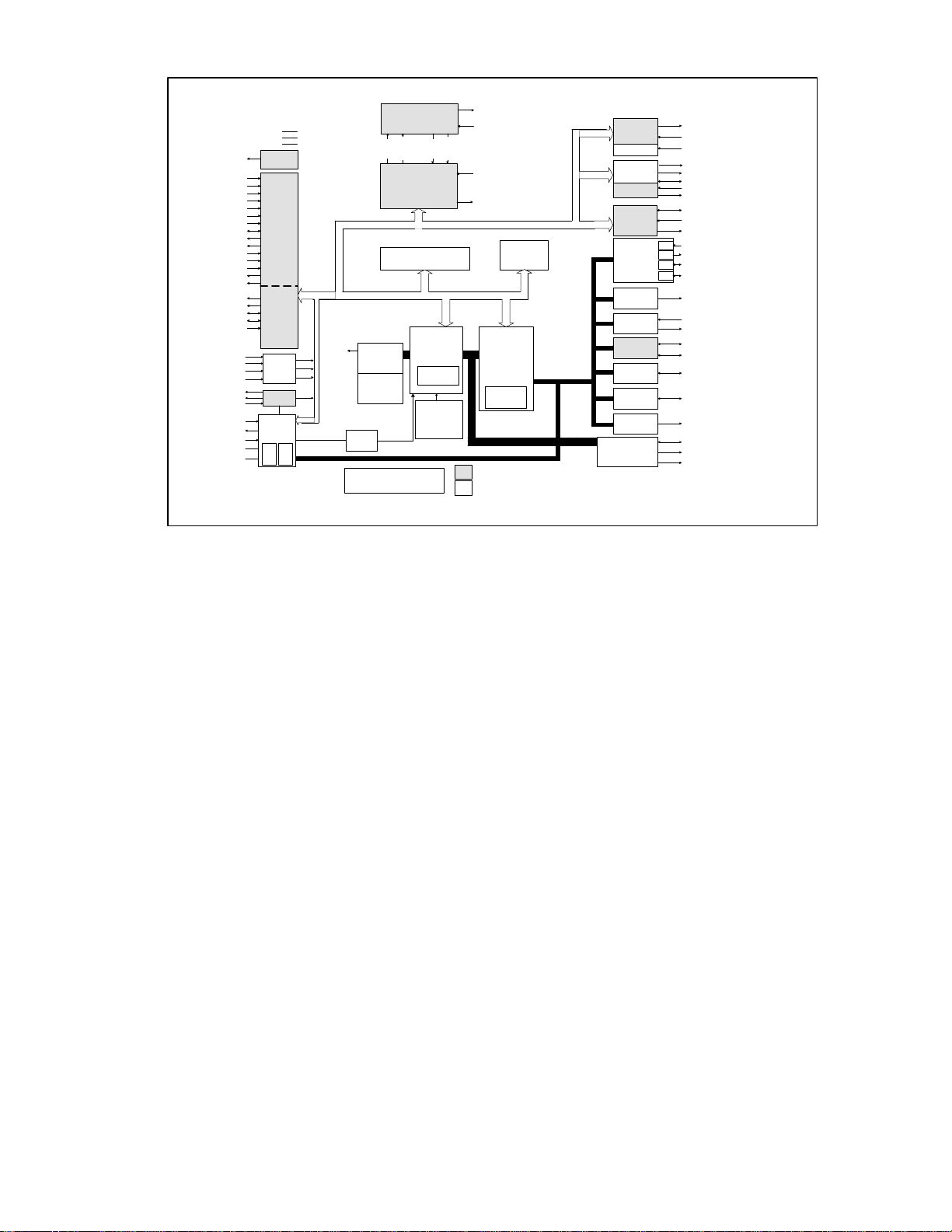
FIGURE 2 - FDC37N972 BLOCK DIAGRAM
10
Page 11

DESCRIPTION OF PIN FUNCTIONS
TABLE 1 - FDC37N972 PIN CONFIGURATION
TQFP
PIN#
1
2
3
4
5
6
7
8
9
10
11
12
13
14
15
16
17
18
19 G3 FPD 57 U3 SA3 95 R13 IOCHRDY
20 H4 IRTX 58 T4 SA4 96 U13 nROMCS
21 G1 IRRX 59 R4 SA5 97 U14 nMEMRD
22 H2 KSO13 60 P5 SA6 98 T14 nMEMWR
23 H3 KSO12 61 U4 SA7 99 R14 PCI_CLK
24 J4 KSO11 62 T5 SA8 100 U15 nCLKRUN
25 H1 KSO10 63 R5 SA9 101 U16 SER_IRQ
26 J2 KSO9 64 P6 SA10 102 T15 nRESET_OUT
27 J3 KSO8 65 U5 SA11 103 R15 CLOCKI
28 K4 KSO7 66 T6 SA12 104 T16 VCC2
29 J1 VCC1 67 R6 SA13 105 U17 24MHz_OUT
30 K2 KSO6 68 P7 SA14 106 R16 nEC_SCI
31 K3 KSO5 69 U6 SA15 107 P14 VSS
32 L4 KSO4 70 T7 OUT0 108 T17 32kHz_OUT
33 K1 KSO3 71 R7 OUT1 109 R17 VCC1_
34 L2 KSO2 72 P8 OUT2 110 P16 nPWR_LED
35 L3 KSO1 73 U7 VSS 111 P15 PWRGD
36 M4 KSO0 74 T8 OUT3 112 N14 SLCT
37 L1 KSI7 75 R8 OUT4 113 P17 PE
38
FGBA
PIN# NAME
A1
VSS 39
C2 OUT5
D4 OUT6
B1 DRVDEN0
C1 DRVDEN1
D2 nMTR0
D3
VSS 45
E4 nDS0
D1 nDIR
E2 nSTEP
E3 nWDATA
F4 nWGATE
E1 nHDSEL
F2 nINDEX
F3 nTRK0
G4 nWRTPRT
F1 nRDATA
G2 nDSKCHG
M2 KSI6
TQFP
PIN#
40
41
42
43
44
46
47
48
49
50
51
52
53
54
55
56
76
FGBA
PIN# NAME
M3 KSI5
N4 KSI4
M1 KSI3
N2 KSI2
N3 KSI1
N1 KSI0
P1 GPIO20
P2 GPIO21
P3 IMCLK
R1 IMDAT
T1
VSS 87
R2 KCLK
R3 KDAT
T2 EMCLK
U1 EMDAT
T3 SA0
P4 SA1
U2 SA2
P9 nNOWS
11
TQFP
PIN#
77
78
79
80
81
82
83
84
85
86
88
89
90
91
92
93
94
114
FGBA
PIN# NAME
U8 nIOR
T9 nIOW
R9 AEN
P10 SD0
U9 SD1
T10 SD2
R10
VCC2
P11 SD3
U10 SD4
T11 SD5
R11 SD6
P12 SD7
U11
VSS
T12 nDACK0
R12 DRQ0
P13 nDACK1
U12 DRQ1
T13 TC
PWRGD
N16 BUSY
Page 12
TQFP
PIN#
115
116
117
118
119
120
121
122
123
124
125
126
127
128
129
130
131
132
133
134
135
136
137
138
139
140
141
142
143
144
145
146
FGBA
PIN# NAME
N15 nACK
M14 PD7
N17 PD6
M16 PD5
M15 PD4
L14
VCC2 152
M17 PD3
L16 PD2
L15 PD1
K14 PD0
L17 NSLCTIN
K16 nINIT
K15 nERROR
J14 nALF
K17 nSTROBE
J16 RXD
J15 TXD
H14
VSS 164
J17 nDSR
H16 nRTS
H15 nCTS
G14 nDTR
H17 nDCD
G16 nRI
G15 GPIO15
F14 GPIO14
G17 GPIO8
F16 GPIO9
F15
VCC1 175
E14 FA18
F17 GPIO10
E16 GPIO11
TQFP
PIN#
147
148
149
150
151
153
154
155
156
157
158
159
160
161
162
163
165
166
167
168
169
170
171
172
173
174
176
177
178
FGBA
PIN# NAME
E15 GPIO12
E17 IN0
D17 IN1
D16 IN2
D15 IN3
C17 IN4
B17 IN5
C16 IN6
C15 IN7
B16
VCC0 188
A17 XOSEL
B15 XTAL1
D14 XTAL2
A16
AGND 192
A15 FAD0
B14 FAD1
C14 FAD2
D13 FAD3
A14 FAD4
B13 FAD5
C13
VSS 199
D12 FAD6
A13 FAD7
B12 FA8
C12 FA9
D11 FA10
A12 FA11
B11 FA12
C11 FA13
D10
VCC1 208
A11 FA14
B10 FA15
TQFP
PIN#
179
180
181
182
183
184
185
186
187
189
190
191
193
194
195
196
197
198
200
201
202
203
204
205
206
207
FGBA
PIN# NAME
C10 FA16
D9 FA17
A10 FALE
B9 nFRD
C9 nFWR
D8 nFCS
A9 GPIO1
B8 GPIO2
C8 GPIO3
D7 GPIO4
A8 GPIO5
B7 GPIO6
C7 GPIO7
D6
VSS
A7 nEA
B6 MODE
C6 AB1_DATA
D5 AB1_CLK
A6 nBAT_LED
B5 nFDD_LED
C5 OUT11
A5 OUT10
A4 OUT9
B4 OUT8
C4 OUT7
A3 GPIO16
A2
VCC2
B3 GPIO17
C3 GPIO18
B2 GPIO19
VCC2 VCC1 VCC0
12
Page 13

Device functions per pin are shown in TABLE 2.
Buffer Modes symbols in TABLE 2 are described
in Table 3. Multifunction pins are summarized
in Table 4, including a multiplex controls
reference.
The pins and descriptions in Table 2 are
organized by primary pin function. For example,
the PS2 Serial Clock and PS2 Serial Data pins
are technically part of the KEYBOARD AND
MOUSE INTERFACE but are listed in the
GENERAL PURPOSE I/O INTERFACE because
the GPIO function of these pins is the default.
TABLE 2 - PIN FUNCTION DESCRIPTION
TQFP
PIN# NOTES NAME DESCRIPTION
POWER
PLANE
BUFFER
MODES
FDD INTERFACE (15)
The following FDC output pins can be configured as either Open Drain outputs capable of sinking 12mA
(OD12) or as push-pull outputs capable of driving 6mA and sinking 12mA (O12). The FDC output pins
must tristate when the FDC is in powerdown mode (The board designer must provide external pull-up
resistors on these output pins).
4 DRVDEN0 Drive Density Select 0 VCC2 (O12/OD12)
5 DRVDEN1 Drive Density Select 1 VCC2 (O12/OD12)
6 nMTR0 Motor On 0 VCC2 (O12/OD12)
8 nDS0 Drive Select 0 VCC2 (O12/OD12)
9 nDIR Step Direction VCC2 (O12/OD12)
10 nSTEP Step Pulse VCC2 (O12/OD12)
11 nWDATA Write Disk Data VCC2 (O12/OD12)
12 nWGATE Write Gate VCC2 (O12/OD12)
13 nHDSEL Head Select VCC2 (O12/OD12)
14 nINDEX Index Pulse Input VCC2 IS
15 nTRK0 Track 0 VCC2 IS
16 nWRTPRT Write Protected VCC2 IS
17 nRDATA Read Disk Data VCC2 IS
18 nDSKCHG Disk Change VCC2 IS
19 FPD Floppy Power Down Output Control VCC2 O8
PCI POWER MANAGEMENT AND SIRQ INTERFACE (4)
106 7 nEC_SCI Power Management Event VCC1 PCI_OD
99 PCI_CLK PCI Clock VCC2 PCI_ICLK
101 SER_IRQ Serial IRQ VCC2 PCI_IO
100 nCLKRUN PCI Clock Control VCC2 PCI_OD
ISA HOST INTERFACE (37)
80: 82,
SD[7:0] System Data Bus VCC2 IO12
84: 88
54: 69 SA[15:0] System Address Bus VCC2 I
96 nROMCS ROM Chip Select VCC2 I
79 AEN Address Enable VCC2 I
95 IOCHRDY I/O Channel Ready VCC2 OD12
91, 93 DRQ[1:0] DMA Requests VCC2 O12
2
13
Page 14

TQFP
PIN# NOTES NAME DESCRIPTION
POWER
PLANE
90, 92 NDACK[1:0] DMA Acknowledge VCC2 I
94 TC Terminal Count VCC2 I
77 nIOR I/O Read VCC2 I
78 nIOW I/O Write VCC2 I
97 nMEMRD Memory Read VCC2 I
98 nMEMWR Memory Write VCC2 I
76 nNOWS No Wait State VCC2 OD12
FLASH ROM INTERFACE (23)
161:
FAD[7:0] Flash Address/Data[7:0] Bus VCC1 IO8
166,
168,
169
170:
175,
177:
FA[8:17] Flash Address[17:8]
NOTE: Upper Address bit FA18 is
multiplexed on GPIO13
VCC1 O8
180
144 5 FA18/
GPIO13
Flash Address 18
General Purpose I/O
VCC1 O8/IO8
(WK_SE17)
182 nFRD Flash Memory Read VCC1 O8
183 nFWR Flash Memory Write VCC1 O8
181 FALE Flash Address Latch Enable VCC1 O8
184 5 nFCS/
GPIO0
Flash ROM Chip Select
General Purpose I/O
VCC1 O8/IO8
(WK_SE02)
KEYBOARD AND MOUSE INTERFACE (29)
30: 36,
24:
28
KSO[0:11]
Keyboard Scan Outputs (14 × 8).
NOTE: GPIO4 and GPIO5 can be
configured as KSO14 and KSO15
VCC1 OD4
(16 × 8).
23 3 KSO12/
OUT8/
KBRST
22 11 KSO13/
GPIO18
Keyboard Scan Output
General Purpose Output
CPU_RESET
Keyboard Scan Output
General Purpose I/O
VCC1 OD4/OD4/
VCC1 OD4/IOD4
37:44 KSI[0:7] Keyboard Scan Inputs VCC1 ISP
193 nEA External Access for 2k ROM VCC1 I
52 EMCLK EM Serial Clock VCC2 IOD16
53 EMDAT EM Serial Data VCC2 IOD16
47 IMCLK IM Serial Clock VCC2 IOD16
48 IMDAT IM Serial Data VCC2 IOD16
51 KDAT Keyboard Data VCC2 IOD16
BUFFER
MODES
OD4
2
14
Page 15

TQFP
PIN# NOTES NAME DESCRIPTION
POWER
PLANE
BUFFER
MODES
50 KCLK Keyboard Clock VCC2 IOD16
GENERAL PURPOSE I/O INTERFACE (40)
70 7,8 OUT0 (SCI) General Purpose Output (SCI) VCC1 (O12/OD12)
71 3 OUT1/
nIRQ8
General Purpose Output/
Active Low RTC IRQ
VCC1 O12/O12
72 OUT2 General Purpose Output VCC1 O12
74 OUT3/
FRW
General Purpose Output
Inverted Flash ROM Memory Write
VCC1 O12/O12
75 OUT4 General Purpose Output VCC1 O12
2 3 OUT5/
nDS1/
KBRST
3 3 OUT6/
nMTR1
203 3 OUT7/
nSMI
202 3 OUT8/
DRQ2/
KBRST
201 3 OUT9/
DRQ3
200 OUT10/
PWM0
199 OUT11/
PWM1
148 4 IN0
General Purpose Output
FDD Drive Select 1
CPU_RESET
3
3
General Purpose Output
VCC1 O12/(O12/
VCC1 O12/(O12/
FDD Motor On 1
General Purpose Output
VCC1 O12/OD12
SMI Output
General Purpose Output
VCC1 O12/O12/
DMA Request
CPU_RESET
General Purpose Output
VCC1 O12/O12
DMA Request
General Purpose Output
VCC1 O12/O12
Pulse Width Modulator Output
General Purpose Output
VCC1 O12/O12
Pulse Width Modulator Output
General Purpose Input VCC1 I
OD12)/O12
OD12)
O12
(WK_EE4)
149 4 IN1
General Purpose Input VCC1 I
(WK_EE2)
150 4 IN2
General Purpose Input VCC1 I
(WK_EE3)
151 IN3
(nGPWKUP)
152 5 IN4
General Purpose Input (General
VCC1 I
Purpose Wake Up)
General Purpose Input VCC1 I
(WK_SE00)
153 5 IN5
General Purpose Input VCC1 I
(WK_SE01)
154 5 IN6
General Purpose Input VCC1 I
(WK_SE05)
155 4 IN7
General Purpose Input VCC1 I
(WK_EE1)
185 5 GPIO1
General Purpose I/O VCC1 IO8
(WK_SE03)
15
2
Page 16

TQFP
PIN# NOTES NAME DESCRIPTION
186 5 GPIO2
General Purpose I/O VCC1 IO8
(WK_SE04)
187 6 GPIO3
(TRIGGER)
188 5 GPIO4
(WK_SE07)/
General Purpose I/O (Interrupt 1
Event)
General Purpose I/O
Keyboard Scan Output
KSO14
189 5 GPIO5
(WK_SE10)/
General Purpose I/O
Keyboard Scan Output
KSO15
190 5 GPIO6
(WK_SE11)/
IRMODE/IRR
General Purpose I/O
FIR Mode Output or 2nd Receive
Input
X3A
191 5, 8 GPIO7
(WK_SE06)
141 5 GPIO8
(WK_SE12)/
General Purpose I/O VCC1 (IO8/IOD8)
5
General Purpose I/O
IR Receive Input
IRRX2
142 1,
5
GPIO9
(WK_SE13)/
General Purpose I/O
IR Transmit Output
IRTX2
145 5 GPIO10
(WK_SE14)/
IRMODE/IRR
General Purpose I/O
FIR Mode Output or 2nd Receive
Input
X3B
146 5 GPIO11
(WK_SE15)/
General Purpose I/O
ACCESS.bus 2 Serial Data
AB2_DATA
147 5 GPIO12
(WK_SE16)/
General Purpose I/O
ACCESS.bus 2 Clock
AB2_CLK
140 5 GPIO14
General Purpose I/O VCC1 IO8
(WK_SE20)
139 5 GPIO15
General Purpose I/O VCC1 IO8
(WK_SE21)
204 5 GPIO16
(WK_SE22)
206 3,
5
GPIO17
(WK_SE23)/
General Purpose I/O VCC1 IO8
5
General Purpose I/O
KBD GATEA20 Output
GATEA20
POWER
PLANE
BUFFER
MODES
VCC1 IO8
VCC1 IO8/OD8
VCC1 IO8/OD8
VCC1 IO8/(O8/I)
VCC1 IO8/I
VCC1 IO12/O12
VCC1 IO8/O8/
(O8/I)
VCC1 IO12/IOD12
VCC1 IO12/IOD12
VCC1 IO8/O8
2
8
16
Page 17

TQFP
PIN# NOTES NAME DESCRIPTION
207 5 GPIO18
(WK_SE27)/
General Purpose I/O/
DMA Acknowledge
POWER
PLANE
VCC1 IO8/I
nDACK2
208 5 GPIO19
(WK_SE24)/
General Purpose I/O/
DMA Acknowledge
VCC1 IO8/I
nDACK3
45 3,
5
GPIO20
(WK_SE25)/
PS2CLK/
General Purpose I/O
PS2 Serial Clock
8051 RX Input
VCC1 IOD16/
IOD16/I
8051RX/
46 3,5 GPIO21
(WK_SE26)/
PS2DAT/
General Purpose I/O
PS2 Serial Data
8051 TX Input
VCC1 IOD16/
IOD16/
OD16
8051TX
INFRARED INTERFACE (2)
21 IRRX IR Receive Input VCC1 I
20 1 IRTX IR Transmit Output VCC2 O12
PARALLEL PORT INTERFACE (17)
126 nINIT/
nDIR
125 nSLCTIN/
nSTEP
124 PD0/
nINDEX
123 PD1/
nTRK0
122 PD2/
nWRTPRT
121 PD3/
nRDATA
119 PD4/
nDSKCHG
Initiate Output
FDC Direction Control
Printer Select Input
FDC Step Pulse
Port Data 0
FDC Index
Port Data 1
FDC Track 0
Port Data 2
FDC Write Protected
Port Data 3
FDC Read Disk Data
Port Data 4
FDC Disk Change
VCC2 (OD14/
OP14)/OD14
VCC2 (OD14/
OP14)/OD14
VCC2 IOP14/I
VCC2 IOP14/I
VCC2 IOP14/I
VCC2 IOP14/I
VCC2 IOP14/I
118 PD5 Port Data 5 VCC2 IOP14
117 PD6/
nMTR0
Port Data 6
FDC Motor On 0
VCC2 IOP14/OD14
116 PD7 Port Data 7 VCC2 IOP14
112 SLCT/
nWGATE
113 PE/
nWDATA
114 BUSY/
nMTR1
Printer Selected Status
FDC Write Gate
Paper End
FDC Write Data
Busy
FDC Motor On 1
VCC2 I/OD12
VCC2 I/OD12
VCC2 I/OD12
BUFFER
MODES
2
17
Page 18

TQFP
PIN# NOTES NAME DESCRIPTION
115 nACK/
nDS1
127 nERROR/
nHDSEL
128 nALF/
DRVDEN0
129 nSTROBE/
nDS0
Acknowledge
FDC Drive Select 1
Error
FDC Head Select
Autofeed Output
FDC Density Select 0
Strobe Output
FDC Drive Select 0
POWER
PLANE
VCC2 I/OD12
VCC2 I/OD12
VCC2
VCC2
SERIAL PORT INTERFACE (8)
130 RXD Receive Data VCC2 I
131 TXD Transmit Data VCC2 O12
133 nDSR Data Set Ready VCC2 I
134 nRTS Request to Send VCC2 O8
135 nCTS Clear to Send VCC2 I
136 nDTR Data Terminal Ready VCC2 O8
138 nRI Ring Indicator VCC1 I
137 nDCD Data Carrier Detect VCC2 I
MISCELLANEOUS (11)
108 32kHz_OUT 32.768kHz Output Clock --The 32
VCC1 O8
KHz output is enabled / disabled by
setting / clearing bit-0 of the Output
Enable 8051 memory mapped
register. When disabled the 32
KHz_OUT pin is driven low. The 32
KHz_OUT pin defaults to the
disabled state on VCC1 POR.
105 24MHz_OUT 24MHz Clock Output
VCC2 O24
Programmable Clock Output.
1.8432 MHz (default = 24 MHz/13)
14.318 MHz
16 MHz
24 MHz
48 MHz
103 CLOCKI 14.318MHz Clock Input VCC2 ICLK
194 MODE Configuration Ports Base Address
VCC1 I
Select
157 10 XOSEL External 32kHz Clock Enable Input VCC0 I
BUFFER
MODES
(OD14/OP14)/
OD14
(OD14/OP14)/
OD14
2
18
Page 19

TQFP
PIN# NOTES NAME DESCRIPTION
109 9 VCC1_PWRGDVCC1 Power Good Input. The
POWER
PLANE
VCC1 IP
BUFFER
MODES
trailing edge of VCC1 POR is
released 20ms from the assertion of
this pin. If this pin is pulled low
while VCC1 is valid, then VCC1
POR will be asserted and held until
20ms from re-assertion of this pin.
This pin has an internal weak
(90µA) pull-up to VCC1.
102
nRESET_OUT
System Reset VCC2 O8
197 nBAT_LED Battery LED (0 = ON) VCC1 OD12
110 nPWR_LED Power LED (0 = ON) VCC1 OD12
198 nFDD_LED Floppy LED (0 = ON). This pin is
VCC1 OD12
asserted whenever either DRVSEL1
or DRVSEL0 is asserted or
controlled by the 8051.
111 9 PWRGD VCC2 Power Good Input VCC1 I
ACCESS BUS INTERFACE (2)
195 AB1_DATA ACCESS.bus 1 Serial Data VCC1 IOD12
196 AB1_CLK ACCESS.bus 1 Clock VCC1 IOD12
REAL TIME CLOCK INTERFACE (2)
158 XTAL1 32.768kHz Crystal Input VCC0 ICLK2
159 10 XTAL2 32.768kHz Crystal Output VCC0 (OCLK2/I)
POWER PLANES
156 VCC0 RTC (V
29,
VCC1
+3.3V ± 5% Main Battery Supply
) Supply Voltage
BAT
143,
176,
83,
104,
VCC2
+3.3V ± 5% Switched AC/Main
Battery Supply
120,
205
160 AGND Analog Ground
1,7,49,
VSS Digital Ground
73, 89,
107,
132,
167,
192
2
19
Page 20

NOTE 1: These pins default to “output”, “low” to prevent infrared transceiver damage (see
Section IRTX Output Pins DEFAULT).
NOTE 2: Buffer Modes per function on multiplexed pins are separated by a slash “/”; e.g., a
pin with two multiplexed functions where the primary function is an input and the
secondary function is an 8mA bidirectional driver is represented as “I/IO8”. Buffer
Modes in parenthesis represent multiple buffer modes for a single pin function.
NOTE 3: This pin is tristated when PWRGD is inactive and the pin is configured as a VCC2-
powered alternate function.
NOTE 4: These devices can generate wake-up events on either edge of the signal that is
applied when the pin is configured as an input. The interrupts are masked by the
Wake-up Mask Register bits.
NOTE 5: These devices can generate wake-up events on selectable edges of the signal that is
applied when the pin is configured as an input. The interrupts are masked by the
Wake-up Mask Registers and selected edges are programmed via the Edge Select
registers (see section 8051 Internal PARALLEL on page 170).
NOTE 6: This interrupt is masked by INT1 Mask Register bit 3. GPIO3 is the only GPIO pin
which does not generate a wakeup event.
NOTE 7: The nEC_SCI pin can be controlled by hardware and 8051 software. The nEC_SCI
pin can drive either the ACPI Run-time GPE Chipset input or the Wake GPE Chipset
input (FIGURE 7). Depending how the nEC_SCI pin is used, other ACPI-related SCI
functions may be best supplied by FDC37N972 general purpose output OUT0.
NOTE 8: OUT0 and GPIO7 are suitable as an SCI output pin because the buffer type can be
configured as a push-pull or open-drain output (see a description of the MISC21 and
MISC23 bits in Multiplexing_3 Register on page 278).
NOTE 9: Input levels for the PWRGD and VCC1_PWRGD pins are rail-to-rail ±400mV; e.g.,
PWRGD VIL = .4V max, PWRGD VIH = 2.7V min. @ VCC1 min.
NOTE 10: The function of these pins are described in Section 32kHz Clock Input
The FDC37N972 uses the XOSEL pin to select either a 32.768kHz input clock or a
32.768kHz crystal to drive the Real Time Clock Interface (Table 2 - PIN FUNCTION
DESCRIPTION).
When XOSEL = ‘0’, the RTC uses a 32.768kHz crystal connected between the
XTAL1 and XTAL2 pins. When XOSEL = ‘1’, the RTC is driven by a 32.768kHz
single-ended clock source connected to THE XTAL2 PIN.
NOTE: ICC0 ≥≥ 10µA for time-keeping operations under VCC0 using a single-ended
clock source. ICC1 = 30µA under VCC1 using a single-ended clock source.
NOTE 11: The GPIO18 alternate function of the KS013 pin has no wake-up capability (see note
following).
20
Page 21

TABLE 3 - BUFFER MODE LEGEND
BUFFER SYMBOL DESCRIPTION
I Input
IO12 Bidirectional – 12mA sink, 6mA source
IO8 Bidirectional – 8mA, 4mA source
IOD16 Input, open drain output – 16mA sink
IOD8 Input, open drain output – 8mA sink
IOP14 Bidirectional – 14mA sink, 14mA source, backdrive
protected
IP Input with pullup
IS Schmitt trigger input
ISP Schmitt trigger input with pullup
O12 Output – 12mA, 6mA source
O8 Output – 8mA, 4mA source
OD12 Open drain – 12mA sink
OD14 Open drain – 14mA sink
OD16 Open drain – 16mA sink
OD4 Open drain – 4mA sink
OD8 Open drain – 8mA sink
OP14 Output – 14mA sink, 14mA source, backdrive protected
PCI_ICLK PCI clock input
PCI_IO PCI bidirectional
PCI_OD PCI open drain
ICLK Clock input
ICLK2 Clock input 2
OCLK2 Clock output 2
O24 Output – 12mA, 6mA source
21
Page 22

TABLE 4 - ALTERNATE FUNCTION PINS
DEFAULT
FUNCTION
2
OUT1 VCC1 nIRQ8
OUT3 VCC1 FWR VCC1 - - ALT WRITE
OUT5 VCC1 nDS1
OUT6 VCC1 nMTR1
OUT7 VCC1 nSMI
OUT8 VCC1 DRQ2
OUT9 VCC1 DRQ3
OUT10 VCC1 PWM0 VCC1 - MISC4
OUT11 VCC1 PWM1 VCC1 - MISC12
nFCS VCC1 GPIO0 VCC1 - MISC19
GPIO4 VCC1 KSO14 VCC1 -
ALTERNATE
FUNCTION #1
3
VCC2 - MISC0
3
3
VCC2 KBRST3VCC2 MISC[5, 22]
3
VCC2 - - MISC5
VCC2 - MISC18
3
VCC2 KBRST3VCC2 MISC[17,10,
3
VCC2 - MISC11
ALTERNATE
FUNCTION #2
MULTIPLEX
CONTROLS
SELECT
6
1
6]
1
1
MISC9
GPIO5 VCC1 KSO15 VCC1 GPIO6 VCC1 IRMODE/IR
GPIO8 VCC1 IRRX VCC1 GPIO9 VCC1 IRTX
GPIO10 VCC1 IRMODE/IR
RX3A
RX3B
3
4
3
GPIO11 VCC1 AB2_DATA VCC1
GPIO12 VCC1 AB2_CLK VCC1
FA18 VCC1 GPIO13 VCC1 - MISC8
GPIO17 VCC1 GATEA20
VCC2 - MISC[14:13]
VCC2 VCC2 - MISC[16:15]
3
VCC1 - MISC6
MISC[2,7]
MISC20
1
GPIO18 VCC1 nDACK2 VCC1 - MISC17
GPIO19 VCC1 nDACK3 VCC1 - MISC11
GPIO20 VCC1 PS2CLK
GPIO21 VCC1 PS2DAT
3
VCC2 8051RX VCC1
3
VCC2 8051TX VCC1
MISC[3, 1]
KSO12 VCC1 OUT8 VCC1 KBRST3VCC2 MISC[17, 10,
6]
KSO13 VCC1 GPIO18 VCC1 - MISC17
5
22
Page 23

DEFAULT
FUNCTION
2
ALTERNATE
FUNCTION #1
ALTERNATE
FUNCTION #2
MULTIPLEX
CONTROLS
nINIT VCC2 nDIR VCC2 -
nSLCTIN VCC2 nSTEP VCC2 -
CR25[4:3]
PD0 VCC2 nINDEX VCC2 PD1 VCC2 nTRK0 VCC2 PD2 VCC2 nWRTPRT VCC2 PD3 VCC2 nRDATA VCC2 PD4 VCC2 nDSKCHG VCC2 PD6 VCC2 nMTR0 VCC2 -
SLCT VCC2 nWGATE VCC2 -
PE VCC2 nWDATA VCC2 -
BUSY VCC2 nMTR1 VCC2 -
nACK VCC2 NDS1 VCC2 -
nERROR VCC2 NHDSEL VCC2 -
nALF VCC2 DRVDEN0 VCC2 -
nSTROBE VCC2 NDS0 VCC2 -
NOTE 1: See a description in Section MULTIFUNCTION PIN on page 271.
NOTE 2: The FDC37N972 pins are identified by primary pin function (see
DESCRIPTION OF PIN FUNCTIONS on page 11). Note that some functions are
available on more than one pin; e.g., OUT8, GPIO18 and KBRST.
NOTE 3: When this pin is configured as an alternate function output and PWRGD is inactive,
i.e. VCC2 is 0v, the pin will tri-state to prevent back-biasing of external circuitry (see
Section General Purpose I/O (GPIO) on page 265).
NOTE 4: This pin defaults to “output”, “low” for both the default (GPIO) function and the
alternate (IRTX) function, regardless of the state of PWRGD (see Section General
Purpose I/O (GPIO) on page 265).
NOTE 5: MISC5 must be inactive for MISC22 to enable KBRST.
NOTE 6: The ALT WRITE SELECT bit is in the Flash Configuration Register (see Section
ALT WRITE SELECT Bit, D3 on page 197).
23
Page 24

There are three power planes in the FDC37N972
V
CC0, VCC1,
and V
with the following power
CC2
sequencing requirement:
1. V
simultaneously with or after V
2. V
simultaneously with or after V
All internal components which utilize V
shall have power applied
CC2
shall have power applied
CC1
CC1
CC0
.
.
CC0
power
plane are switched internally between the VCC1
and VCC0 pins according to VCC1_PWRGD
See Table 5 for power consumption in various
states.
Two FDC37N972 power supply configurations
can be utilized. These power supply
configuration types fundamentally differ upon
the need for a backup battery (V
to V
.
CC0
) connection
BAT
TYPE 1 devices do not require a V
CC0
battery
connection. Power supply requirements for
TYPE 1 devices are as follows: V
VSS, V
supply, and V
is connected to the main battery
CC1
is switched from either the
CC2
is tied to
CC0
main battery or AC power if available. In this
configuration all internal components which
utilize V
power plane are switched internally
CC0
to the VCC1 upon POR according to
VCC1_PWRGD.
TYPE 2 devices require a V
CC0
battery
connection. Power supply requirements for
TYPE 2 devices are as follows: V
connected to a backup battery (V
BAT
connected to the main battery supply, and V
), V
CC0
CC1
is
is
CC2
is switched from either the main battery or AC
power if available. In this configuration all
internal components which utilize V
plane only when V
is absent. Normally (when
CC1
CC0
power
VCC1_PWRGD is asserted) they are switched
internally to the VCC1 power plane.
24
Page 25

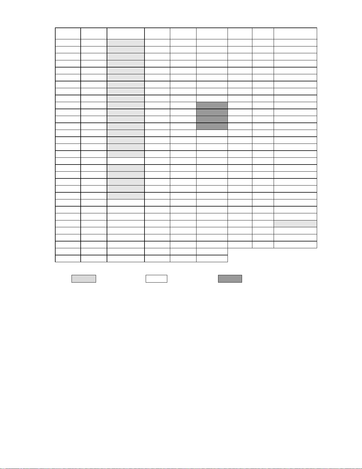
TABLE 5 - POWER COMSUMPTION IN VARIOUS STATES
V
CC2
(VDC)
3.3 3.3 Run 24 MHz I
3.3 3.3 Run 12 MHz I
3.3 3.3 Run Ring
3.3 3.3 Idle Ring
0 3.3 Run Ring
0 3.3 Idle Ring
0 3.3 Sleep Stop I
0 3.3 Sleep Stop I
0 0 I
V
CC1
(VDC)
8051
STATE
CLOCK
STATE
OSC
OSC
OSC
OSC
SYM TYP MAX COMMENTS
I
I
I
I
I
I
I
I
I
I
CC2
CC1
CC2
CC1
CC2
CC1
CC2
CC1
CC2
CC1
CC2
CC1
CC1
CC1
CC0
15 ma
24 ma
13 ma
12 ma
>1ma
8 ma
>1ma
5 ma
8 ma 10 ma
6 ma 8 ma
5 µa 10 µa XOSEL=0
40 µa 60 µa 2.4 < V
20 ma
30 ma
15 ma
18 ma
2 ma
10 ma
2 ma
FLOPPY @ 1 Meg Data Rate
I2C @ 24 MHz
Floppy @ 500K Data Rate
I2C @ 12 MHz
PLL On
I2C Off
PLL Off
7 ma
PLL Off
I2C Off
PLL Off
I2C Off
160 µa XOSEL=1
cc0
< 4 VDC,
XOSEL=1,
0 0 I
CC0
0.4 µa 1.5 µa 2.4 < V
< 4 VDC,
cc0
XOSEL = 0
Note: When a single-ended 32.768kHz clock source is selected (see Section 32kHz Clock Input).
The FDC37N972 uses the XOSEL pin to select either a 32.768kHz input clock or a
32.768kHz crystal to drive the Real Time Clock Interface (Table 2 - PIN FUNCTION
DESCRIPTION). When XOSEL = ‘0’, The RTC uses a 32.768kHz crystal connected between
the XTAL1 and XTAL2 pins. When XOSEL = ‘1’, the RTC is driven by a 32.768kHz singleended clock source connected to the XTAL2 pin.
25
Page 26

TABLE 7 - POWER PIN LIST
BIAS PINS
156 VCC0 RTC (V
)Supply Voltage 2.7-3.3V ibat<2ma
BAT
29, 143, 176 VCC1 8051 + AB + CI + RTC+ ACPI + PM1 + WDT + MR + CR
+ PM + AB2 + FI + PWM + KI + GPIO + LED + IR + 3.3V
+/-5% Supply Voltage (Note)
83, 104, 120, 205 VCC2 SR + PCG + FDC + DDS + UART + PP + PS/2 + Core
+3.3V +/-5%Supply Voltage
160 AGND Analog Ground for VCC0.
1, 7, 49, 73, 89,
VSS Digital Ground
107, 132, 167, 192
Note:
AB = ACCESS.bus
CI = Control Inputs
WDT = Watch Dog Timer
MR = Mailbox Registers
CR = Control Registers
PM = Power Management
AB2 = ACCESS.BUS2
FI = Flash Interface
KI = Keyboard Interface
GPIO = General Purpose I/O Interface
IR = Infrared
SR = System Reset
PCG = PLL Clock Generator
FDC = Floppy Disk Controller
DDS = Digital Data Seperator
PP = Multi-Mode Parallel Port
PWRGD and VCC1_PWRGD timing is illustrated in FIGURE 3 through FIGURE 5.
26
Page 27
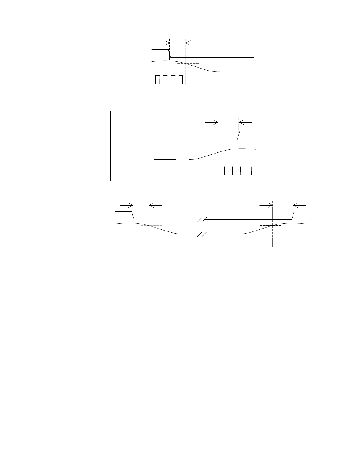
10µs
PWRGD
VCC2
CLOCKI
min.
3V
FIGURE 3 – POWER-FAIL EVENT
PWRGD
10µs
min.
VCC2
CLOCKI
3V
FIGURE 4 - VCC2 POWER-UP TIMING
1µs
min.
VCC1_PWRGD
VCC1
3V 3V
FIGURE 5 - VCC1_PWRGD TIMING
These figures also appear in the “Timing Diagrams” section of this spec.
1µs
min.
27
Page 28

FUNCTIONAL DESCRIPTION
FDC37N972 OPERATING REGISTERS
The address map, shown below in TABLE 8,
shows the set of operating registers and
addresses for each of the logical blocks of the
FDC37N972 Ultra I/O controller. The base
addresses of the FDC, Parallel, Serial 1 and
Infrared ports can be moved via the
configuration registers.
TABLE 8 - FDC37N972 OPERATING REGISTER ADDRESSES
LOGICAL
DEVICE
NUMBER
0x00 FDC [0x100:0x0FF8]
0x03 Parallel
LOGICAL
DEVICE
Port
BASE I/O
RANGE
(NOTE3)
ON 8 BYTE
BOUNDARIES
[0x100:0x0FFC]
ON 4 BYTE
BOUNDARIES
(EPP Not supported)
or
[0x100:0x0FF8]
ON 8 BYTE
BOUNDARIES
(all modes
supported,
EPP is only available
when the base
address is on an 8byte boundary)
HOST PROCESSOR INTERFACE
The host processor communicates with the
FDC37N972 through a series of read/write
registers. The range of base I/O port addresses
for these registers is shown in TABLE 8.
Register access is accomplished through
programmed I/O or DMA transfers. All registers
are 8 bits. Most of the registers support zero
wait-state access (NOWS). All host interface
output buffers are capable of sinking a minimum
of 6 mA.
ISA
FIXED
BASE OFFSETS
+0 : SRA
+1 : SRB
+2 : DOR
+3 : TSR
+4 : MSR/DSR
+5 : FIFO
+7 : DIR/CCR
+0 : Data / ecpAfifo
+1 : Status
+2 : Control
+400h : cfifo / ecpDfifo
tfifo / cnfgA
+401h : cnfgB
+402h : ecr
CYCLE
TYPE
NOWS
Std. ISA I/O
28
Page 29

LOGICAL
DEVICE
NUMBER
LOGICAL
DEVICE
0x04 Serial
BASE I/O
RANGE
(NOTE3)
[0x100:0x0FF8]
Port 1
ON 8 BYTE
BOUNDARIES
0x05 Infrared
[0x100:0x0FF8]
Port
ON 8 BYTE
BOUNDARIES
0x62,
0x63
[0x100:0x0FF8]
ON 8 BYTE
BOUNDARIES
0x06 RTC Not Relocatable
Fixed Base Address
0x07 KYBD Not Relocatable
Fixed Base
Address
FIXED
BASE OFFSETS
+0 : RB/TB LSB div
+1 : IER MSB div
+2 : IIR/FCR
+3 : LCR
+4 : MCR
+5 : LSR
+6 : MSR
+7 : SCR
+0 : RB/TB LSB div
+1 : IER MSB div
+2 : IIR/FCR
+3 : LCR
+4 : MCR
+5 : LSR
+6 : MSR
+7 : SCR
+0 : Register Block N,
address 0
+1 : Register Block N,
address 1
+2 : Register Block N,
address 2
+3 : Register Block N,
address 3
+4 : Register Block N,
address 4
+5 : Register Block N,
address 5
+6 : Register Block N,
address 6
+7 : SCE Master Control
Reg.
0x70, 0x74 : Address
Register
0x71, 0x76 : Data Register
0x60 : Data Register
0x64 : Command/Status
Reg.
ISA
CYCLE
TYPE
NOWS
NOWS
NOWS
Std. ISA I/O
NOWS
Note 1: Refer to the configuration register descriptions for setting the base address
Note 2: This chip uses all ISA address bits to decode the base address of each of its logical devices.
29
Page 30

FLOPPY DISK CONTROLLER
The Floppy Disk Controller (FDC) provides the
interface between a host microprocessor and
the Floppy Disk Drives (FDD). The FDC
integrates the functions of the
formatter/controller, Digital Data Separator,
Write Precompensation and data rate Selection
logic for an IBM XT/AT compatible FDC. The
true CMOS 765B core guarantees 100% IBM
PC XT/AT compatibility in addition to providing
data overflow and underflow protection.
TABLE 9 - STATUS, DATA AND CONTROL REGISTERS
FDC PRIMARY BASE I/O
ADDRESS OFFSET R/W REGISTER
0 R Status Register A (SRA)
1 R Status Register B (SRB)
2 R/W Digital Output Register (DOR)
3 R/W Tape Drive Register (TDR)
4 R Main Status Register (MSR)
4 W Data Rate Select Register (DSR)
5 R/W Data (FIFO)
6 Reserved
7 R Digital Input Register (DIR)
7 W Configuration Control Register (CCR)
The FDC is compatible to the 82077AA using
SMSC's proprietary FDC core.
FDC INTERNAL REGISTERS
The FDC contains eight internal registers, which
facilitate the interfacing between the host
microprocessor and the disk drive TABLE 9
shows the addresses required toaccess these
registers. Registers other than the ones shown
are not supported.
STATUS REGISTER A (SRA)
FDC I/O BASE ADDRESS + 0x00
(READ ONLY)
This register is read-only and monitors the state of the FDC Interrupt pin and several disk
interface pins in PS/2 and Model 30 modes. The SRA can be accessed at any time when in PS/2
mode. In the PC/AT mode the data bus pins D0 - D7 are held in a high impedance state for a read of
SRA.
30
Page 31

TABLE 10 - SRB - PS/2 MODEL 30 MODE
7 6 5 4 3 2 1 0
INT
PENDING
RESET
COND.
BIT 0 DIRECTION
Active high status indicating the direction of head movement. A logic "1" indicates inward direction; a
logic "0" indicates outward direction.
BIT 1 nWRITE PROTECT
Active low status of the WRITE PROTECT disk interface input. A logic "0" indicates that the disk is
write protected.
BIT 2 nINDEX
Active low status of the INDEX disk interface input.
BIT 3 HEAD SELECT
Active high status of the HDSEL disk interface input. A logic "1" selects side 1 and a logic "0" selects
side 0.
BIT 4 nTRACK 0
Active low status of the TRK0 disk interface input.
BIT 5 STEP
Active high status of the STEP output disk interface output pin.
0 N/A 0 N/A 0 N/A N/A 0
nDRV2 STEP nTRK0 HDSEL nINDX nWP DIR
BIT 6 nDRV2
Active low status of the DRV2 disk interface input pin, indicating that a second drive has been
installed.
BIT 7 INTERRUPT PENDING
Active high bit indicating the state of the Floppy Disk Interrupt output.
31
Page 32

TABLE 11 - SRA - PS/2 MODEL 30 MODE
7 6 5 4 3 2 1 0
INT
PENDING
RESET
COND.
BIT 0 nDIRECTION
Active low status indicating the direction of head movement. A logic "0" indicates inward direction; a
logic "1" indicates outward direction.
BIT 1 WRITE PROTECT
Active high status of the WRITE PROTECT disk interface input. A logic "1" indicates that the disk is
write protected.
BIT 2 INDEX
Active high status of the INDEX disk interface input.
BIT 3 nHEAD SELECT
Active low status of the HDSEL disk interface input. A logic "0" selects side 1 and a logic "1" selects
side 0.
BIT 4 TRACK 0
Active high status of the TRK0 disk interface input.
BIT 5 STEP
Active high status of the latched STEP disk interface output pin. This bit is latched with the STEP
output going active, and is cleared with a read from the DIR register, or with a hardware or software
reset.
0 0 0 N/A 1 N/A N/A 1
DRQ STEP
F/F
TRK0 NHDSELINDX WP nDIR
BIT 6 DMA REQUEST
Active high status of the FDC’s DRQ output pin.
BIT 7 INTERRUPT PENDING
Active high bit indicating the state of the Floppy Disk Interrupt output.
32
Page 33

DIGITAL OUTPUT REGISTER (DOR)
FDC I/O BASE ADDRESS + 0X02 (READ/WRITE)
The DOR controls the drive select and motor enables of the disk interface outputs. It also contains
the enable for the DMA logic and a software reset bit. The contents of the DOR are unaffected by a
software reset. The DOR can be written to at any time.
TABLE 12 - FDC DOR
7 6 5 4 3 2 1 0
MOT
EN3
RESET
COND.
BIT 0 and 1 DRIVE SELECT
These two bits are binary encoded for the two drive selects output pins nds0 and nds1, thereby
allowing only one drive to be selected at one time.
BIT 2 nreset
A logic “0” written to this bit resets the FDC. This reset will remain active until a logic “1” is written to
this bit. This software reset does not affect the DSR and CCR registers, nor does it affect the other
bits of the DOR register. The minimum reset duration required is 100ns, therefore toggling this bit by
consecutive writes to this register is a valid method of issuing a software reset.
BIT 3 DMAEN
PC/AT and Model 30 Mode: Writing this bit to logic “1” will enable the FDC’s ndack and TC inputs and
enable the FDC’s DRQ and Interrupt outputs. This bit being a logic “0” will disable the FDC’s ndack
and TC inputs, and hold the FDC’s DRQ and Interrupt outputs in a high impedance state. This bit is a
logic “0” after a reset.
PS/2 Mode: In this mode the TC and the FDC’s DRQ, ndack, and Interrupt pins are always enabled.
During a reset, the DRQ, ndack, TC, and Interrupt pins will remain enabled, but this bit will be cleared
to a logic “0”.
MOT
EN2
0 0 0 0 0 0 0 0
MOT
EN1
MOT
EN0
DMAEN nRESETDRIVE
SEL1
DRIVE
SEL0
BIT 4 MOTOR ENABLE 0
This bit controls the nmtr0 disk interface output. A logic “1” in this bit will cause the output pin to
assert.
BIT 5 MOTOR ENABLE 1
This bit controls the nmtr1 disk interface output. A logic “1” in this bit will cause the output pin to
assert.
BIT 6 MOTOR ENABLE 2
This bit controls the nmtr2 disk interface output. A logic “1” in this bit will cause the output pin to
assert.
BIT 7 MOTOR ENABLE 3
This bit controls the nmtr3 disk interface output. A logic “1” in this bit will cause the output pin to
assert.
33
Page 34

TABLE 13 – FDC SRB – PS/2 MODEL 30 MODE
7 6 5 4 3 2 1 0
RESET
nDRV2 nDS1 nDS0 WDATA
F/F
N/A 1 1 0 0 0 1 1
RDATA
F/F
WGATE
F/F
nDS3 nDS2
COND.
TABLE 14 - FDC DOR
7 6 5 4 3 2 1 0
RESET
MOT
EN3
0 0 0 0 0 0 0 0
MOT
EN2
MOT
EN1
MOT
EN0
DMAEN nRESET DRIVE
SEL1
DRIVE
SEL0
COND.
BIT 0 and 1 DRIVE SELECT
These two bits are binary encoded for the two drive selects output pins nds0 and nds1, thereby
allowing only one drive to be selected at one time.
BIT 2 nRESET
A logic “0” written to this bit resets the FDC. This reset will remain active until a logic “1” is written to
this bit. This software reset does not affect the DSR and CCR registers, nor does it affect the other
bits of the DOR register. The minimum reset duration required is 100ns, therefore toggling this bit by
consecutive writes to this register is a valid method of issuing a software reset.
BIT 3 DMAEN
PC/AT and Model 30 Mode:
Writing this bit to logic “1” will enable the FDC’s nDACK and TC inputs and enable the FDC’s DRQ
and Interrupt outputs. This bit being a logic “0” will disable the FDC’s nDACK and TC inputs, and hold
the FDC’s DRQ and Interrupt outputs in a high impedance state. This bit is a logic “0” after a reset.
PS/2 Mode: In this mode the TC and the FDC’s DRQ, and Interrupt pins are always enabled. During
a reset, the DRQ, TC, and Interrupt pins will remain enabled, but this bit will be cleared to a logic “0”.
BIT 4 MOTOR ENABLE 0
This bit controls the disk interface output. A logic “1” in this bit will cause the output pin to assert.
BIT 5 MOTOR ENABLE 1
This bit controls the nMTR1 disk interface output. A logic “1” in this bit will cause the output pin to
assert.
BIT 6 MOTOR ENABLE 2
This bit controls the nMTR2 disk interface output. A logic “1” in this bit will cause the output pin to
assert.
BIT 7 MOTOR ENABLE 3
This bit controls the nMTR3 disk interface output. A logic “1” in this bit will cause the output pin to
assert.
34
Page 35

TABLE 13 – FDC INTERNAL 2 DRIVE DECODE – DRIVES 0 AND 1 SWAPPED
DRIVE SELECT
DIGITAL OUTPUT REGISTER
Bit 7 Bit 6 Bit 5 Bit 4 Bit1 Bit 0 Nds1 Nds0 Nmtr1 Nmtr0
X X X 1 0 0 0 1 Nbit 4 Nbit 5
X X 1 X 0 1 1 0 Nbit 4 Nbit 5
X 1 X X 1 0 1 1 Nbit 4 Nbit 5
1 X X X 1 1 1 1 Nbit 4 Nbit 5
0 0 0 0 X X 1 1 Nbit 4 Nbit 5
OUTPUTS (ACTIVE
LOW)
MOTOR ON OUTPUTS
(ACTIVE LOW)
TAPE DRIVE REGISTER (TDR)
FDC I/O BASE ADDRESS + 0x03
(READ/WRITE)
This register is included for 82077 software
compatability. The TDR is unaffected by a
software reset. The improved data separator
incorporates tape drive support and requires the
Tape Select bits in the FDC Tape Drive register
to identify which drive has been assigned to
receive this support (see the following section).
TABLE 14 - FDC TDR NORMAL FLOPPY MODE
DB7 DB6 DB5 DB4 DB3 DB2 DB1 DB0
REG 3F3 Tri-state Tri-state Tri-state Tri-state Tri-state Tri-state tape sel 1 tape sel 0
TAPE SEL1
(TDR.1)
0 0 None
0 1 1
1 0 2
1 1 3
NORMAL FLOPPY MODE
Normal mode. The TDR allows the user to
assign tape support to a particular drive during
initialization. Any future references to that drive
number automatically invokes tape support.
The Tape Select bits are TDR[1:0]. The TDR
Register contains only bits 0 and 1. When this
register is read, bits 2 – 7 are a high impedance.
TAPE SEL2
(TDR.0)
DRIVE
SELECTED
35
Page 36

ENHANCED FLOPPY MODE 2 (OS2)
The TDR Register for Enhanced Floppy Mode 2 operation.
TABLE 15 - FDC TDR ENHANCED FLOPPY MODE 2 (OS2)
DB7 DB6 DB5 DB4 DB3 DB2 DB1 DB0
REG 3F3 1 1 Drive Type ID Floppy Boot Drive tape sel1 tape sel0
BIT 7 This bit is always set active high
BIT 6 This bit is always set active high
BITS 5 and 4 Drive Type ID
These bits reflect two of the bits of L0-CRF1 (Logical Device 0 – Configuration Register 0xF1).
Which two bits these are depends on the last drive selected in the Digital Output Register. (See
TABLE 20)
BITS 3 and 2 Floppy Boot Drive
These bits reflect two of the bits of L0-CRF1. Bit 3 = L0-CRF1-B7. Bit 2 = L0-CRF1-B6.
BIT 1 and 0 – Tape Drive Select (READ/WRITE)
Same as in Normal and Enhanced Floppy Mode 2.
TABLE 16 – DRIVE TYPE ID
DIGITAL OUTPUT REGISTER TDR REGISTER – DRIVE TYPE ID
Bit 1 Bit 0 Bit 5 Bit 4
0 0 L0-CRF2 – B1 L0-CRF2 – B0
0 1 L0-CRF2 – B3 L0-CRF2 – B2
1 0 L0-CRF2 – B5 L0-CRF2 – B4
1 1 L0-CRF2 – B7 L0-CRF2 – B6
Note: L0-CRF2-Bx = Logical Device 0, Configuration Register F2, Bit x.
MID[1:0] FDD INTERFACE PINS
The FDC Media ID pins are not supported in the FDC37N972. The MID[1:0] inputs to the FDC core
are strapped so that the Media ID bits the TDR are always “high”.
36
Page 37

DATA RATE SELECT REGISTER (DSR)
FDC I/O BASE ADDRESS + 0x04 (WRITE
ONLY)
This register is write only. It is used to program
the data rate, amount of write precompensation,
power down status, and software reset. The
data rate is programmed using the
Configuration Control Register (CCR) not the
DSR, for PC/AT and PS/2 Model 30 and
TABLE 17 - FDC DSR
7 6 5 4 3 2 1 0
S/W
RESET
RESET
COND.
BITS 0 - 1 DATA RATE SELECT
These bits control the data rate of the floppy controller. See TABLE 19 for the settings corresponding
to the individual data rates. The data rate select bits are unaffected by a software reset and are set to
250 Kbps after a hardware reset.
BITS 2 - 4 PRECOMPENSATION SELECT
These three bits select the value of write precompensation that will be applied to the WDATA output
signal. TABLE 18 shows the precompensation values for the combination of these bits settings.
Track 0 is the default starting track number to start precompensation. This starting track number can
be changed by the configure command.
POWER
DOWN
0 0 0 0 0 0 1 0
0 PRE-
Microchannel applications. Other applications
can set the data rate in the DSR. The data rate
of the floppy controller is the most recent write
of either the DSR or CCR. The DSR is
unaffected by a software reset. A hardware
reset will set the DSR to 02H, which
corresponds to the default precompensation
setting and 250 Kbps.
COMP2
PRE-
COMP1
PRE-
COMP0
DRATE
SEL1
DRATE
SEL0
BIT 5 UNDEFINED
Should be written as a logic "0".
BIT 6 LOW POWER
A logic "1" written to this bit will put the floppy controller into manual low power mode. The floppy
controller clock and data separator circuits will be turned off. The controller will come out of manual
low power mode after a software reset or access to the Data Register or Main Status Register.
BIT 7 SOFTWARE RESET
This active high bit has the same function as the DOR RESET (DOR bit 2) except that this bit is self
clearing.
37
Page 38

TABLE 18 - FDC PRECOMPENSATION DELAYS
PRECOMPENSATION
PRECOMP 432
DELAY (nsec)
<2Mbps 2Mbps
111
001
010
011
100
101
110
000
0.00
41.67
83.34
125.00
166.67
208.33
250.00
Default
0
20.8
41.7
62.5
83.3
104.2
125
Default
Default: See TABLE 16
TABLE 19 – FDC DATA RATES
DRIVE RATE DATA RATE DATA RATE DENSEL DRATE(1)
DRT1 DRT0 SEL1 SEL0 MFM FM 1 0
0 0 1 1 1Meg --- 1 1 1
0 0 0 0 500 250 1 0 0
0 0 0 1 300 150 0 0 1
0 0 1 0 250 125 0 1 0
0 1 1 1 1Meg --- 1 1 1
0 1 0 0 500 250 1 0 0
0 1 0 1 500 250 0 0 1
0 1 1 0 250 125 0 1 0
1 0 1 1 1Meg --- 1 1 1
1 0 0 0 500 250 1 0 0
1 0 0 1 2Meg --- 0 0 1
1 0 1 0 250 125 0 1 0
Drive Rate Table (Recommended) 00 = 360K, 1.2M, 720K, 1.44M and 2.88M Vertical Format
01 = 3-Mode Drive
10 = 2 Meg Tape
Note 1: The DRATE and DENSEL values are mapped onto the DRIVEDEN pins.
38
Page 39

TABLE 20 - FDC DRVDEN MAPPING
DT1 DT0 DRVDEN1 (1) DRVDEN0 (1) DRIVE TYPE
0 0 DRATE0 DENSEL 4/2/1 MB 3.5"
2/1 MB 5.25" FDDS
2/1.6/1 MB 3.5" (3-MODE)
1 0 DRATE0 DRATE1
0 1 DRATE0 nDENSEL PS/2
1 1 DRATE1 DRATE0
TABLE 21 - FDC DEFAULT PRECOMPENSATION DELAYS
PRECOMPENSATION
DATA RATE
2 Mbps
1 Mbps
500 Kbps
300 Kbps
250 Kbps
DELAYS
20.8 ns
41.67 ns
125 ns
125 ns
125 ns
39
Page 40

MAIN STATUS REGISTER
FDC I/O BASE ADDRESS + 0x04
(READ ONLY)
The Main Status Register is a read-only register
and indicates the status of the disk controller.
The Main Status Register can be read at any
TABLE 22 - FDC MSR
7 6 5 4 3 2 1 0
RQM DIO NON
DMA
BIT 0 - 3 DRVx BUSY
These bits are set to 1s when a drive is in the seek portion of a command, including implied and
overlapped seeks and recalibrates.
BIT 4 COMMAND BUSY
This bit is set to a “1” when a command is in progress. This bit will go active after the command byte
has been accepted and goes inactive at the end of the results phase. If there is no result phase (Seek,
Recalibrate commands), this bit is returned to a “0” after the last command byte.
BIT 5 NON-DMA
This mode is selected in the SPECIFY command and will be set to a “1” during the execution phase of
a command. This is for polled data transfers and helps differentiate between the data transfer phase
and the reading of result bytes.
BIT 6 DIO
Indicates the direction of a data transfer once a RQM is set. A “1” indicates a read and a “0” indicates
a write is required.
CMD
BUSY
time. The MSR indicates when the disk
controller is ready to receive data via the Data
Register. It should be read before each byte
transferring to or from the data register except in
DMA mode. No delay is required when reading
the MSR after a data transfer.
DRV3
BUSY
DRV2
BUSY
DRV1
BUSY
DRV0
BUSY
BIT 7 RQM
Indicates that the host can transfer data if set to a “1”. No access is permitted if set to a “0”.
40
Page 41

DATA REGISTER (FIFO)
FDC I/O BASE ADDRESS + 0x05
(READ/WRITE)
All command parameter information, disk data
and result status are transferred between the
host processor and the FDC through the Data
Register. Data transfers are governed by the
RQM and DIO bits in the Main Status Register.
The Data Register defaults to FIFO disabled
mode after any form of reset. This maintains
PC/AT hardware compatibility. The default
values can be changed through the Configure
command (enable full FIFO operation with
threshold control). The advantage of the FIFO
is that it allows the system a larger DMA latency
without causing a disk error.
TABLE 23 - FIFO SERVICE DELAY
FIFO THRESHOLD
EXAMPLES
1 byte
2 bytes
8 bytes
15 bytes
1 x 4 ms - 1.5 ms = 2.5 ms
2 x 4 ms - 1.5 ms = 6.5 ms
8 x 4 ms - 1.5 ms = 30.5 ms
15 x 4 ms - 1.5 ms = 58.5 ms
TABLE 31 gives several examples of the delays
with a FIFO. The data is based upon the
following formula:
Threshold # x [8/DATA RATE] - 1.5ms = Delay
At the start of a command, the FIFO action is
always disabled and command parameters
must be sent based upon the RQM and DIO bit
settings. As the command execution phase is
entered, the FIFO is cleared of any data to
ensure that invalid data is not transferred.
An overrun or underrun will terminate the
current command and the transfer of data. Disk
writes will complete the current sector by
generating a 00 pattern and valid CRC. Reads
require the host to remove the remaining data
so that the result phase may be entered.
MAXIMUM DELAY TO SERVICING
AT 2 Mbps* DATA RATE
FIFO THRESHOLD
EXAMPLES
1 byte
2 bytes
8 bytes
15 bytes
FIFO THRESHOLD
EXAMPLES
1 byte
2 bytes
8 bytes
15 bytes
MAXIMUM DELAY TO SERVICING
AT 1 Mbps DATA RATE
1 x 8 ms - 1.5 ms = 6.5 ms
2 x 8 ms - 1.5 ms = 14.5 ms
8 x 8 ms - 1.5 ms = 62.5 ms
15 x 8 ms - 1.5 ms = 118.5 ms
MAXIMUM DELAY TO SERVICING
AT 500 Kbps DATA RATE
1 x 16 ms - 1.5 ms = 14.5 ms
2 x 16 ms - 1.5 ms = 30.5 ms
8 x 16 ms - 1.5 ms = 126.5 ms
15 x 16 ms - 1.5 ms = 238.5 ms
41
Page 42

DIGITAL INPUT REGISTER (DIR)
FDC I/O BASE ADDRESS + 0X07 (READ ONLY)
This register is read-only in all modes.
DIR - PC-AT Mode
TABLE 24 - FDC DIR ALL MODES
7 6 5 4 3 2 1 0
DSK
CHG
RESET
COND.
BIT 0 – 6 UNDEFINED
The data bus outputs D0 – 6 will remain in a high impedance state during a read of this register.
BIT 7 DSKCHG
This bit monitors the pin of the same name and reflects the opposite value seen on the disk cable.
N/A N/A N/A N/A N/A N/A N/A N/A
DIR – PS/2 MODE
TABLE 25 - FDC DIR PS/2 MODE
7 6 5 4 3 2 1 0
DSK CHG 1 1 1 1 DRATE SEL1 DRATE SEL0 nHIGH DENS
RESET
COND.
N/A N/A N/A N/A N/A N/A N/A 1
BIT 0 nhigh DENS
This bit is low whenever the 500 Kbps or 1 Mbps data rates are selected, and high when 250 Kbps and
300 Kbps are selected.
BITS 1 – 2 DATA RATE SELECT
These bits control the data rate of the floppy controller. See TABLE 19for the settings corresponding
to the individual data rates. The data rate select bits are unaffected by a software reset, and are set to
250 Kbps after a hardware reset.
BITS 3 – 6 UNDEFINED
Always read as a logic “1”
BIT 7 DSKCHG
This bit monitors the pin of the same name and reflects the opposite value seen on the disk cable.
42
Page 43

DIR – MODEL 30 MODE
TABLE 26 - FDC DIR MODEL 30 MODE
7 6 5 4 3 2 1 0
DSK
CHG
RESET
COND.
BITS 0 and 1 DATA RATE SELECT
These bits control the data rate of the floppy controller. See TABLE 19 for the settings corresponding
to the individual data rates. The data rate select bits are unaffected by a software reset and are set to
250 Kbps after a hardware reset.
BIT 2 nOPREC
This bit reflects the value of nOPREC bit set in the CCR register.
BIT 3 DMAEN
This bit reflects the value of DMAEN bit set in the DOR register bit 3.
BITS 4 - 6 UNDEFINED
Always read as a logic "0"
BIT 7 DSKCHG
This bit monitors the pin of the same name and reflects the opposite value seen on the pin.
N/A 0 0 0 0 0 1 0
0 0 0 DMAEN nOPREC DRATE
SEL1
DRATE
SEL0
CONFIGURATION CONTROL REGISTER (CCR)
FDC I/O BASE ADDRESS + 0x07
(WRITE ONLY)
TABLE 27 - FDC CCR PC/AT AND PS/2 MODE
7 6 5 4 3 2 1 0
DRATE
SEL1
RESET
COND.
BIT 0 and 1 DATA RATE SELECT 0 and 1
These bits determine the data rate of the floppy controller. See TABLE 19 for the appropriate values.
BIT 2 - 7 RESERVED
Should be set to a logical "0"
N/A N/A N/A N/A N/A N/A 1 0
43
DRATE
SEL0
Page 44

TABLE 28 - FDC CCR - PS/2 MODEL 30 MODE
7 6 5 4 3 2 1 0
NOPREC DRATE
SEL1
RESET
COND.
BIT 0 and 1 DATA RATE SELECT 0 and 1
These bits determine the data rate of the floppy controller. See TABLE 19 for the appropriate values.
BIT 2 NO PRECOMPENSATION
This bit can be set by software, but it has no functionality. It can be read by bit 2 of the DSR when in
Model 30 register mode. Unaffected by software reset.
BIT 3 - 7 RESERVED
Should be set to a logical "0". TABLE 19 shows the state of the DENSEL pin. The DENSEL pin is set
high after a hardware reset and is unaffected by the DOR and the DSR resets.
N/A N/A N/A N/A N/A N/A 1 0
DRATE
SEL0
STATUS REGISTER ENCODING
During the Result Phase of certain commands, the Data Register contains data bytes that give the
status of the command just executed.
TABLE 29 - FDC STATUS REGISTER 0
BIT NO. SYMBOL NAME DESCRIPTION
7,6 IC Interrupt Code 00 - Normal termination of command. The specified
command was properly executed and completed
without error.
01 - Abnormal termination of command. Command
execution was started, but was not successfully
completed.
10 - Invalid command. The requested command could
not be executed.
11 - Abnormal termination caused by Polling.
5 SE Seek End The FDC completed a Seek, Relative Seek or
Recalibrate command (used during a Sense Interrupt
Command).
4 EC Equipment
Check
3 Unused. This bit is always "0".
2 H Head Address The current head address.
1,0 DS1,0 Drive Select The current selected drive.
The TRK0 pin failed to become a "1" after:
Step pulses in the Recalibrate command.
The Relative Seek command caused the FDC to step
outward beyond Track 0.
44
Page 45

TABLE 30 - FDC STATUS REGISTER 1
BIT NO. SYMBOL NAME DESCRIPTION
7 EN End of Cylinder The FDC tried to access a sector beyond the final sector of
the track (255D). Will be set if TC is not issued after Read
or Write Data command.
6 Unused. This bit is always "0".
5 DE Data Error The FDC detected a CRC error in either the ID field or the
data field of a sector.
4 OR Overrun/
Underrun
3 Unused. This bit is always "0".
2 ND No Data Any one of the following:
1 NW Not Writable WP pin became a "1" while the FDC is executing a Write
0 MA Missing Address
Mark
Becomes set if the FDC does not receive CPU or DMA
service within the required time interval, resulting in data
overrun or underrun.
Read Data, Read Deleted Data command - the FDC did not
find the specified sector.
Read ID command - the FDC cannot read the ID field
without an error.
Read A Track command - the FDC cannot find the proper
sector sequence.
Data, Write Deleted Data, or Format A Track command.
Any one of the following:
The FDC did not detect an ID address mark at the specified
track after encountering the index pulse from the IDX pin
twice.
The FDC cannot detect a data address mark or a deleted
data address mark on the specified track.
45
Page 46

TABLE 31 - FDC STATUS REGISTER 2
BIT NO. SYMBOL NAME DESCRIPTION
7 Unused. This bit is always "0".
6 CM Control Mark Any one of the following:
Read Data command - the FDC encountered a deleted
data address mark.
Read Deleted Data command - the FDC encountered a
data address mark.
5 DD Data Error in
Data Field
4 WC Wrong
Cylinder
3 Unused. This bit is always "0".
2 Unused. This bit is always "0".
1 BC Bad Cylinder The track address from the sector ID field is different
0 MD Missing Data
Address Mark
TABLE 32 - FDC STATUS REGISTER 3
BIT NO. SYMBOL NAME DESCRIPTION
7 UNUSED. THIS BIT IS ALWAYS "0".
6 WP Write Protected Indicates the status of the WP pin.
5 Unused. This bit is always "1".
4 T0 Track 0 Indicates the status of the TRK0 pin.
3 Unused. This bit is always "1".
2 HD Head Address Indicates the status of the HDSEL pin.
1,0 DS1,0 Drive Select Indicates the status of the nDS1, nDS0 pins.
The FDC detected a CRC error in the data field.
The track address from the sector ID field is different
from the track address maintained inside the FDC.
from the track address maintained inside the FDC and
is equal to FF hex, which indicates a bad track with a
hard error according to the IBM soft-sectored format.
The FDC cannot detect a data address mark or a
deleted data address mark.
FDC RESET
There are three sources of system reset on the
FDC: the nRESET_OUT bit of the 8051’s Output
enable Register (which controls the
nRESET_OUT pin of the FDC37N972); a reset
generated via a bit in the DOR; and a reset
generated via a bit in the DSR. At VCC2 power
on, a VCC2 Power On Reset initializes the FDC.
All resets take the FDC out of the power down
state.
All operations are terminated upon a RESET,
and the Floppy Disk Controller enters an idle
state. A reset while a disk write is in progress
will corrupt the data and CRC.
On exiting the reset state, various internal
registers are cleared, including the Configure
command information, and the Floppy Disk
Controller waits for a new command. Drive
polling will start unless disabled by a new
Configure command.
46
Page 47

nRESET_OUT PIN (HARDWARE RESET)
The nRESET_OUT pin is a global reset and
clears all registers except those programmed by
the Specify command. The DOR reset bit is
enabled and must be cleared by the host to exit
the reset state.
DOR RESET VS. DSR RESET (SOFTWARE
RESET)
These two resets are functionally the same.
Both will reset the FDC core, which affects drive
status information and the FIFO circuits. The
DSR reset clears itself automatically while the
DOR reset requires the host to manually clear it.
DOR reset has precedence over the DSR reset.
The DOR reset is set automatically upon a
nRESET_OUT pin reset. The user must
manually clear this reset bit in the DOR to exit
the reset state.
FDC MODES OF OPERATION
The FDC has three modes of operation, PC/AT
mode, PS/2 mode and Model 30 mode. These
are determined by the state of IDENT and MFM,
bits[3] and [2] respectively of L0-CRF0.
PC/AT MODE - (IDENT high, MFM a "don't
care")
The PC/AT register set is enabled, the DMA
enable bit of the DOR becomes valid (The
FDC’s IRQ and DRQ can be hi-Z), and TC and
DENSEL become active high signals.
PS/2 MODE - (IDENT low, MFM high)
This mode supports the PS/2 models 50/60/80
configuration and register set. The DMA bit of
the DOR becomes a "don't care", (the FDC’s
IRQ and DRQ are always valid), TC and
DENSEL become active low.
MODEL 30 MODE - (IDENT low, MFM low)
This mode supports PS/2 Model 30
configuration and register set. The DMA enable
bit of the DOR becomes valid (The FDC’s IRQ
and DRQ can be hi-Z), TC is active high and
DENSEL is active low.
DMA TRANSFERS
DMA transfers are enabled with the Specify
command and are initiated by the FDC by
activating its DRQ pin during a data transfer
command. The FIFO is enabled directly by
asserting nDACK and addresses need not be
valid.
Note that if the DMA controller (i.e. 8237A) is
programmed to function in verify mode, a
pseudo read is performed by the FDC based
only on nDACK. This mode is only available
when the FDC has been configured into byte
mode (FIFO disabled) and is programmed to do
a read. With the FIFO enabled, the FDC can
perform the above operation by using the Verify
command; no DMA operation is needed.
CONTROLLER PHASES
For simplicity, command handling in the FDC
can be divided into three phases: Command,
Execution, and Result. Each phase is described
in the following sections.
COMMAND PHASE
After a reset, the FDC enters the command
phase and is ready to accept a command from
the host. For each of the commands, a defined
set of command code bytes and parameter
bytes has to be written to the FDC before the
command phase is complete. (Please refer to
TABLE 33 for the command set descriptions).
These bytes of data must be transferred in the
order prescribed.
Before writing to the FDC, the host must
examine the RQM and DIO bits of the Main
Status Register. RQM and DIO must be equal
to "1" and "0" respectively before command
bytes may be written. RQM is set false by the
FDC after each write cycle until the received
47
Page 48

byte is processed. The FDC asserts RQM again
to request each parameter byte of the command
unless an illegal command condition is
detected. After the last parameter byte is
received, RQM remains "0" and the FDC
automatically enters the next phase as defined
by the command definition.
The FIFO is disabled during the command
phase to provide for the proper handling of the
"Invalid Command" condition.
EXECUTION PHASE
All data transfers to or from the FDC occur
during the execution phase, which can proceed
in DMA or non-DMA mode as indicated in the
Specify command.
Non-DMA Mode - Transfers from the FIFO to
the Host
The FDC’s IRQ pin and RQM bits in the Main
Status Register are activated when the FIFO
contains (16-<threshold>) bytes or the last bytes
of a full sector have been placed in the FIFO.
The FDC’s IRQ pin can be used for interruptdriven systems, and RQM can be used for
polled systems. The host must respond to the
request by reading data from the FIFO. This
process is repeated until the last byte is
transferred out of the FIFO. The FDC will
deactivate the FDC’s IRQ pin and RQM bit when
the FIFO becomes empty.
Non-DMA Mode - Transfers from the Host to the
FIFO
After a reset, the FIFO is disabled. Each data
byte is transferred by an FDC IRQ or DRQ
depending on the DMA mode. The Configure
command can enable the FIFO and set the
FIFO threshold value.
The following paragraphs detail the operation of
the FIFO flow control. In these descriptions,
<threshold> is defined as the number of bytes
available to the FDC when service is requested
from the host and ranges from 1 to 16. The
parameter FIFOTHR, which the user programs,
is one less and ranges from 0 to 15.
A low threshold value (i.e. 2) results in longer
periods of time between service requests, but
requires faster servicing of the request for both
read and write cases. The host reads (writes)
from (to) the FIFO until empty (full), then the
transfer request goes inactive. The host must
be very responsive to the service request. This
is the desired case for use with a "fast" system.
A high value of threshold (i.e. 12) is used with a
"sluggish" system by affording a long latency
period after a service request, but results in
more frequent service requests.
The FDC’s IRQ pin and RQM bit in the Main
Status Register are activated upon entering the
execution phase of data transfer commands.
The host must respond to the request by writing
data into the FIFO. The FDC’s IRQ pin and
RQM bit remain true until the FIFO becomes
full. They are set true again when the FIFO has
<threshold> bytes remaining in the FIFO. The
FDC’s IRQ pin will also be deactivated if TC and
nDACK both go inactive. The FDC enters the
result phase after the last byte is taken by the
FDC from the FIFO (i.e. FIFO empty condition).
DMA Mode - Transfers from the FIFO to the
Host
The FDC activates the FDC’s DRQ pin when the
FIFO contains (16 - <threshold>) bytes, or the
last byte of a full sector transfer has been
placed in the FIFO. The DMA controller must
respond to the request by reading data from the
FIFO. The FDC will deactivate the FDC’s DRQ
pin when the FIFO becomes empty. FDC’s
DRQ goes inactive after nDACK goes active for
the last byte of a data transfer (or on the active
edge of nIOR, on the last byte, if no edge is
present on nDACK). A data underrun may
48
Page 49

occur if the FDC’s DRQ is not removed in time
to prevent an unwanted cycle.
DMA Mode - Transfers from the Host to the
FIFO
The FDC activates the FDC’s DRQ pin when
entering the execution phase of the data transfer
commands. The DMA controller must respond
by activating the nDACK and nIOW pins placing
data in the FIFO. The FDC’s DRQ remains
active until the FIFO becomes full. The FDC’s
DRQ is again set true when the FIFO has
<threshold> bytes remaining in the FIFO. The
FDC will also deactivate the FDC’s DRQ pin
when TC becomes true (qualified by nDACK),
indicating that no more data is required. The
FDC’s DRQ goes inactive after nDACK goes
active for the last byte of a data transfer (or on
the active edge of nIOW of the last byte, if no
edge is present on nDACK). A data overrun
may occur if the FDC’s DRQ is not removed in
time to prevent an unwanted cycle.
Data Transfer Termination
Note that when the host is sending data to the
FIFO of the FDC, the internal sector count will
be complete when the FDC reads the last byte
from its side of the FIFO. There may be a delay
in the removal of the transfer request signal of
up to the time taken for the FDC to read the last
16 bytes from the FIFO. The host must tolerate
this delay.
RESULT PHASE
The generation of the FDC’s IRQ determines the
beginning of the result phase. For each of the
commands, a defined set of result bytes has to
be read from the FDC before the result phase is
complete. These bytes of data must be read out
for another command to start.
RQM and DIO must both equal "1" before the
result bytes may be read. After all the result
bytes have been read, the RQM and DIO bits
switch to "1" and "0" respectively, and the CB bit
is cleared, indicating that the FDC is ready to
accept the next command.
The FDC supports terminal count explicitly
through the TC pin and implicitly through the
underrun/overrun and end-of-track (EOT)
functions. For full sector transfers, the EOT
parameter can define the last sector to be
transferred in a single or multi-sector transfer.
If the last sector to be transferred is a partial
sector, the host can stop transferring the data in
mid-sector, and the FDC will continue to
complete the sector as if a hardware TC was
received. The only difference between these
implicit functions and TC is that they return
"abnormal termination" result status. Such
status indications can be ignored if they were
expected.
COMMAND SET/DESCRIPTIONS
Commands can be written whenever the FDC is
in the command phase. Each command has a
unique set of needed parameters and status
results. The FDC checks to see that the first
byte is a valid command and, if valid, proceeds
withthe command. If it is invalid, an interrupt is
issued. The user sends a Sense Interrupt
Status command which returns an invalid
command error. Refer to Table 33 for
explanations of the various symbols used.
TABLE 34 lists the required parameters and the
results associated with each command that the
FDC is capable of performing.
49
Page 50

TABLE 33 - DESCRIPTION OF THE FDC COMMAND SYMBOLS
SYMBOL NAME DESCRIPTION
C Cylinder Address The currently selected address; 0 to 255.
D Data Pattern The pattern to be written in each sector data field during
formatting.
D0, D1, D2,D3Drive Select 0-3 Designates which drives are perpendicular drives on the
Perpendicular Mode Command. A "1" indicates a perpendicular
drive.
DIR Direction Control If this bit is 0, then the head will step out from the spindle during a
relative seek. If set to a 1, the head will step in toward the spindle.
DS0, DS1 Disk Drive Select
DS1 DS0 DRIVE
0
0
1
1
0
1
0
1
drive 0
drive 1
drive 2
drive 3
DTL Special Sector
Size
By setting N to zero (00), DTL may be used to control the number
of bytes transferred in disk read/write commands. The sector size
(N = 0) is set to 128. If the actual sector (on the diskette) is larger
than DTL, the remainder of the actual sector is read but is not
passed to the host during read commands; during write
commands, the remainder of the actual sector is written with all
zero bytes. The CRC check code is calculated with the actual
sector. When N is not zero, DTL has no meaning and should be
set to FF HEX.
EC Enable Count When this bit is "1" the "DTL" parameter of the Verify command
becomes SC (number of sectors per track).
EFIFO Enable FIFO This active low bit when a 0, enables the FIFO. A "1" disables the
FIFO (default).
EIS Enable Implied
Seek
When set, a seek operation will be performed before executing any
read or write command that requires the C parameter in the
command phase. A "0" disables the implied seek.
EOT End of Track The final sector number of the current track.
GAP Alters Gap 2 length when using Perpendicular Mode.
GPL Gap Length The Gap 3 size. (Gap 3 is the space between sectors excluding
the VCO synchronization field).
H/HDS Head Address Selected head: 0 or 1 (disk side 0 or 1) as encoded in the sector
ID field.
HLT Head Load Time The time interval that the FDC waits after loading the head and
before initializing a read or write operation. Refer to the Specify
command for actual delays.
50
Page 51

SYMBOL NAME DESCRIPTION
HUT Head Unload
Time
The time interval from the end of the execution phase (of a read or
write command) until the head is unloaded. Refer to the Specify
command for actual delays.
LOCK Lock defines whether EFIFO, FIFOTHR, and PRETRK parameters
of the CONFIGURE COMMAND can be reset to their default
values by a "software Reset". (A reset caused by writing to the
appropriate bits of either tha DSR or DOR)
MFM MFM/FM Mode
Selector
MT Multi-Track
Selector
A one selects the double density (MFM) mode. A zero selects
single density (FM) mode.
When set, this flag selects the multi-track operating mode. In this
mode, the FDC treats a complete cylinder under head 0 and 1 as
a single track. The FDC operates as this expanded track started
at the first sector under head 0 and ended at the last sector under
head 1. With this flag set, a multitrack read or write operation will
automatically continue to the first sector under head 1 when the
FDC finishes operating on the last sector under head 0.
N Sector Size Code This specifies the number of bytes in a sector. If this parameter is
"00", then the sector size is 128 bytes. The number of bytes
transferred is determined by the DTL parameter. Otherwise the
sector size is (2 raised to the "N'th" power) times 128. All values
up to "07" hex are allowable. "07"h would equal a sector size of
16k. It is the user's responsibility to not select combinations that
are not possible with the drive.
N SECTOR SIZE
128 bytes
256 bytes
512 bytes
1024 bytes
... ...
07 16 Kbytes
NCN New Cylinder
The desired cylinder number.
Number
ND Non-DMA Mode
Flag
When set to 1, indicates that the FDC is to operate in the non-
DMA mode. In this mode, the host is interrupted for each data
transfer. When set to 0, the FDC operates in DMA mode,
interfacing to a DMA controller by means of the DRQ and nDACK
signals.
OW Overwrite The bits D0-D3 of the Perpendicular Mode Command can only be
modified if OW is set to 1. OW id defined in the Lock command.
PCN Present Cylinder
Number
The current position of the head at the completion of Sense
Interrupt Status command.
POLL Polling Disable When set, the internal polling routine is disabled. When clear,
polling is enabled.
51
Page 52

SYMBOL NAME DESCRIPTION
PRETRK Precompensation
Start Track
Number
R Sector Address The sector number to be read or written. In multi-sector transfers,
RCN Relative Cylinder
Number
SC Number of
Sectors Per Track
SK Skip Flag When set to 1, sectors containing a deleted data address mark will
SRT Step Rate Interval The time interval between step pulses issued by the FDC.
ST0
ST1
ST2
ST3
WGATE Write Gate Alters timing of WE to allow for pre-erase loads in perpendicular
Status 0
Status 1
Status 2
Status 3
Programmable from track 00 to FFH.
this parameter specifies the sector number of the first sector to be
read or written.
Relative cylinder offset from present cylinder as used by the
Relative Seek command.
The number of sectors per track to be initialized by the Format
command. The number of sectors per track to be verified during a
Verify command when EC is set.
automatically be skipped during the execution of Read Data. If
Read Deleted is executed, only sectors with a deleted address
mark will be accessed. When set to "0", the sector is read or
written the same as the read and write commands.
Programmable from 0.5 to 8 milliseconds in increments of 0.5 ms
at the 1 Mbit data rate. Refer to the SPECIFY command for actual
delays.
Registers within the FDC which store status information after a
command has been executed. This status information is available
to the host during the result phase after command execution.
drives.
52
Page 53

FDC INSTRUCTION SET
TABLE 34 - FDC INSTRUCTION SET
READ DATA
DATA BUS
PHASE R/W D7 D6 D5 D4 D3 D2 D1 D0 REMARKS
Command W MT MFM SK 0 0 1 1 0 Command Codes
W 0 0 0 0 0 HDS DS1 DS0
W -------- C -------- Sector ID information prior
to Command execution.
W -------- H -------W -------- R -------W -------- N -------W ------- EOT ------W ------- GPL ------W ------- DTL -------
Execution Data transfer between the
FDD and system.
Result R ------- ST0 ------- Status information after
Command execution.
R ------- ST1 ------R ------- ST2 ------R -------- C -------- Sector ID information after
Command execution.
R -------- H -------R -------- R -------R -------- N --------
53
Page 54

READ DELETED DATA
DATA BUS
PHASE R/W D7 D6 D5 D4 D3 D2 D1 D0 REMARKS
Command W MT MFM SK 0 1 1 0 0 Command Codes
W 0 0 0 0 0 HDS DS1 DS0
W -------- C -------- Sector ID information prior to
Command execution.
W -------- H -------W -------- R -------W -------- N -------W ------- EOT ------W ------- GPL ------W ------- DTL -------
Execution Data transfer between the
FDD and system.
DATA BUS
PHASE R/W D7 D6 D5 D4 D3 D2 D1 D0 REMARKS
R ------- ST2 ------R -------- C -------- Sector ID information after
Command execution.
R -------- H -------R -------- R -------R -------- N --------
54
Page 55

WRITE DATA
DATA BUS
PHASE R/W D7 D6 D5 D4 D3 D2 D1 D0 REMARKS
Command W MT MFM 0 0 0 1 0 1 Command Codes
W 0 0 0 0 0 HDS DS1 DS0
W -------- C -------- Sector ID information prior to
Command execution.
W -------- H -------W -------- R -------W -------- N -------W ------- EOT ------W ------- GPL ------W ------- DTL -------
Execution Data transfer between the
FDD and system.
Result R ------- ST0 ------- Status information after
Command execution.
R ------- ST1 ------R ------- ST2 ------R -------- C -------- Sector ID information after
Command execution.
R -------- H -------R -------- R -------R -------- N --------
55
Page 56

WRITE DELETED DATA
DATA BUS
PHASE R/W D7 D6 D5 D4 D3 D2 D1 D0 REMARKS
Command W MT MFM 0 0 1 0 0 1 Command Codes
W 0 0 0 0 0 HDS DS1 DS0
W -------- C -------- Sector ID information
prior to Command
execution.
W -------- H -------W -------- R -------W -------- N -------W ------- EOT ------W ------- GPL ------W ------- DTL -------
Execution Data transfer between
the FDD and system.
Result R ------- ST0 ------- Status information after
Command execution.
R ------- ST1 ------R ------- ST2 ------R -------- C -------- Sector ID information
after Command
execution.
R -------- H -------R -------- R -------R -------- N --------
56
Page 57

READ A TRACK
DATA BUS
PHASE R/W D7 D6 D5 D4 D3 D2 D1 D0 REMARKS
Command W 0 MFM 0 0 0 0 1 0 Command Codes
W 0 0 0 0 0 HDS DS1 DS0
W -------- C -------- Sector ID information
prior to Command
execution.
W -------- H -------W -------- R -------W -------- N -------W ------- EOT ------W ------- GPL ------W ------- DTL -------
DATA BUS
PHASE R/W D7 D6 D5 D4 D3 D2 D1 D0 REMARKS
R ------- ST1 ------R ------- ST2 ------R -------- C -------- Sector ID information
after Command
execution.
R -------- H -------R -------- R -------R -------- N --------
57
Page 58

VERIFY
DATA BUS
PHASE R/W D7 D6 D5 D4 D3 D2 D1 D0 REMARKS
Command W MT MFM SK 1 0 1 1 0 Command Codes
W EC 0 0 0 0 HDS DS1 DS0
W -------- C -------- Sector ID information
prior to Command
execution.
W -------- H -------W -------- R -------W -------- N -------W ------- EOT ------W ------- GPL ------W ------ DTL/SC ------
Execution No data transfer takes
place.
Result R ------- ST0 ------- Status information after
Command execution.
R ------- ST1 ------R ------- ST2 ------R -------- C -------- Sector ID information
after Command
execution.
R -------- H -------R -------- R -------R -------- N --------
58
Page 59

VERSION
DATA BUS
PHASE R/W D7 D6 D5 D4 D3 D2 D1 D0 REMARKS
Command W 0 0 0 1 0 0 0 0 Command Code
Result R 1 0 0 1 0 0 0 0 Enhanced Controller
FORMAT A TRACK
DATA BUS
PHASE R/W D7 D6 D5 D4 D3 D2 D1 D0 REMARKS
Command W 0 MFM 0 0 1 1 0 1 Command Codes
W 0 0 0 0 0 HDS DS1 DS0
W -------- N -------- Bytes/Sector
W -------- SC -------- Sectors/Cylinder
W ------- GPL ------- Gap 3
W -------- D -------- Filler Byte
Execution for
Each Sector
Repeat:
Result R ------- ST0 ------- Status information after
W -------- C -------- Input Sector
Parameters
W -------- H --------
W -------- R -------W -------- N --------
FDC formats an entire
cylinder
Command execution
R ------- ST1 ------R ------- ST2 ------R ------ Undefined -----R ------ Undefined -----R ------ Undefined -----R ------ Undefined ------
59
Page 60

RECALIBRATE
DATA BUS
PHASE R/W D7 D6 D5 D4 D3 D2 D1 D0 REMARKS
Command W 0 0 0 0 0 1 1 1 Command Codes
W 0 0 0 0 0 0 DS1 DS0
Execution Head retracted to Track 0
Interrupt.
SENSE INTERRUPT STATUS
DATA BUS
PHASE R/W D7 D6 D5 D4 D3 D2 D1 D0 REMARKS
Command W 0 0 0 0 1 0 0 0 Command Codes
Result R ------- ST0 ------- Status information at the end
of each seek operation.
R ------- PCN -------
SPECIFY
DATA BUS
PHASE R/W D7 D6 D5 D4 D3 D2 D1 D0 REMARKS
Command W 0 0 0 0 0 0 1 1 Command Codes
W --- SRT --- --- HUT --W ------ HLT ------ ND
SENSE DRIVE STATUS
DATA BUS
PHASE R/W D7 D6 D5 D4 D3 D2 D1 D0 REMARKS
Command W 0 0 0 0 0 1 0 0 Command Codes
W 0 0 0 0 0 HDS DS1 DS0
Result R ------- ST3 ------- Status information about
FDD
SEEK
DATA BUS
PHASE R/W D7 D6 D5 D4 D3 D2 D1 D0 REMARKS
Command W 0 0 0 0 1 1 1 1 Command Codes
W 0 0 0 0 0 HDS DS1 DS0
W ------- NCN -------
Execution Head positioned over
proper cylinder on
diskette.
60
Page 61

CONFIGURE
DATA BUS
PHASE R/W D7 D6 D5 D4 D3 D2 D1 D0 REMARKS
Command W 0 0 0 1 0 0 1 1 Configure
Information
W 0 0 0 0 0 0 0 0
W 0 EIS EFIFO POLL --- FIFOTHR ---
Execution W --------- PRETRK ---------
RELATIVE SEEK
DATA BUS
PHASE R/W D7 D6 D5 D4 D3 D2 D1 D0 REMARKS
Command W 1 DIR 0 0 1 1 1 1
W 0 0 0 0 0 HDS DS1 DS0
W ------- RCN -------
DUMPREG
DATA BUS
PHASE R/W D7 D6 D5 D4 D3 D2 D1 D0 REMARKS
Command W 0 0 0 0 1 1 1 0 *Note:
Registers
placed in
FIFO
Execution
Result R ------ PCN-Drive 0 -------
R ------ PCN-Drive 1 ------R ------ PCN-Drive 2 ------R ------ PCN-Drive 3 ------R ---- SRT ---- --- HUT --R ------- HLT ------- ND
R ------- SC/EOT ------R LOCK 0 D3 D2 D1 D0 GAP WGATE
R 0 EIS EFIFO POLL -- FIFOTHR -R -------- PRETRK --------
61
Page 62

READ ID
DATA BUS
PHASE R/W D7 D6 D5 D4 D3 D2 D1 D0 REMARKS
Command W 0 MFM 0 0 1 0 1 0 Commands
W 0 0 0 0 0 HDS DS1 DS0
Execution The first correct ID
information on the
Cylinder is stored in
Data Register
Result R -------- ST0 -------- Status information after
Command execution.
Disk status after the
Command has
completed
R -------- ST1 -------R -------- ST2 -------R -------- C -------R -------- H -------R -------- R -------R -------- N --------
PERPENDICULAR MODE
DATA BUS
PHASE R/W D7 D6 D5 D4 D3 D2 D1 D0 REMARKS
Command W 0 0 0 1 0 0 1 0 Command Codes
OW 0 D3 D2 D1 D0 GAP WGATE
62
Page 63

INVALID CODES
DATA BUS
PHASE R/W D7 D6 D5 D4 D3 D2 D1 D0 REMARKS
Command W ----- Invalid Codes ----- Invalid Command Codes
(NoOp - FDC goes into
Standby State)
Result R ------- ST0 ------- ST0 = 80H
LOCK
DATA BUS
PHASE R/W D7 D6 D5 D4 D3 D2 D1 D0 REMARKS
Command W LOCK 0 0 1 0 1 0 0 Command Codes
Result R 0 0 0 LOCK 0 0 0 0
SC is returned if the last command that was issued was the Format command. EOT is returned if the
last command was a Read or Write.
Note: These bits are used internally only. They are not reflected in the Drive Select pins. It is the
user's responsibility to maintain correspondence between these bits and the Drive Select pins (DOR).
63
Page 64

FDC DATA TRANSFER COMMANDS
All of the Read Data, Write Data and Verify type
commands use the same parameter bytes and
return the same results information, the only
difference being the coding of bits 0-4 in the first
byte.
An implied seek will be executed if the feature
was enabled by the Configure command. This
seek is completely transparent to the user. The
TABLE 35 - FDC SECTOR SIZES
N SECTOR SIZE
00
01
02
03
..
07
READ DATA
A set of nine (9) bytes is required to place the
FDC in the Read Data Mode. After the Read
Data command has been issued, the FDC loads
the head (if it is in the unloaded state), waits the
specified head settling time (defined in the
Specify command), and begins reading ID
Address Marks and ID fields. When the sector
address read off the diskette matches with the
sector address specified in the command, the
FDC reads the sector's data field and transfers
the data to the FIFO.
After completion of the read operation from the
current sector, the sector address is
incremented by one and the data from the next
logical sector is read and output via the FIFO.
This continuous read function is called "MultiSector Read Operation". Upon receipt of TC, or
an implied TC (FIFO overrun/underrun), the
FDC stops sending data but will continue to
read data from the current sector, check the
CRC bytes, and at the end of the sector,
terminate the Read Data Command.
128 bytes
256 bytes
512 bytes
1024 bytes
...
16 Kbytes
Drive Busy bit for the drive will go active in the
Main Status Register during the seek portion of
the command. If the seek portion fails, it will be
reflected in the results status normally returned
for a Read/Write Data command. Status
Register 0 (ST0) would contain the error code
and C would contain the cylinder on which the
seek failed.
N determines the number of bytes per sector
(see TABLE 35 above). If N is set to zero, the
sector size is set to 128. The DTL value
determines the number of bytes to be
transferred. If DTL is less than 128, the FDC
transfers the specified number of bytes to the
host. For reads, it continues to read the entire
128-byte sector and checks for CRC errors. For
writes, it completes the 128-byte sector by filling
in zeros. If N is not set to 00 Hex, DTL should
be set to FF Hex and has no impact on the
number of bytes transferred.
The amount of data which can be handled with
a single command to the FDC depends upon
MT (multi-track) and N (number of bytes/sector).
The Multi-Track function (MT) allows the FDC to
read data from both sides of the diskette. For a
particular cylinder, data will be transferred
starting at Sector 1, Side 0 and completing the
last sector of the same track at Side 1.
64
Page 65

If the host terminates a read or write operation
in the FDC, the ID information in the result
phase is dependent upon the state of the MT bit
and EOT byte.
At the completion of the Read Data command,
the head is not unloaded until after the Head
Unload Time Interval (specified in the Specify
command) has elapsed. If the host issues
another command before the head unloads,
then the head settling time may be saved
between subsequent reads.
If the FDC detects a pulse on the nINDEX pin
twice without finding the specified sector
(meaning that the diskette's index hole passes
through index detect logic in the drive twice), the
FDC sets the IC code in Status Register 0 to
"01" indicating abnormal termination, sets the
TABLE 36 - EFFECTS OF MT AND N BITS
MAXIMUM TRANSFER
MT
N
0
1
256 x 26 = 6,656
1
1
256 x 52 = 13,312
0
2
512 x 15 = 7,680
1
2
512 x 30 = 15,360
0
3
1024 x 8 = 8,192
1
3
1024 x 16 = 16,384
CAPACITY
ND bit in Status Register 1 to "1" indicating a
sector not found, and terminates the Read Data
Command. After reading the ID and Data Fields
in each sector, the FDC checks the CRC bytes.
Ifa CRC error occurs in the ID or data field, the
FDC sets the IC code in Status Register 0 to
"01" indicating abnormal termination, sets the
DE bit flag in Status Register 1 to "1", sets the
DD bit in Status Register 2 to "1" if CRC is
incorrect in the ID field, and terminates the Read
Data Command.
TABLE 40 - VERIFY COMMAND RESULT
PHASE TABLE describes the effect of the SK
bit on the Read Data command execution and
results. Except where noted in TABLE 36, the C
or R value of the sector address is automatically
incremented (see TABLE 42).
FINAL SECTOR READ
FROM DISK
26 at side 0 or 1
26 at side 1
15 at side 0 or 1
15 at side 1
8 at side 0 or 1
16 at side 1
TABLE 37 - SKIP BIT VS READ DATA COMMAND
DATA ADDRESS
SK BIT
VALUE
MARK TYPE
ENCOUNTERED RESULTS
SECTOR
READ?
CM BIT OF
ST2 SET?
DESCRIPTION OF
RESULTS
0 Normal Data Yes No Normal termination
1 Deleted Data No Yes Normal termination.
Sector not read
("skipped")
65
Page 66

READ DELETED DATA
This command is the same as the Read Data
command, only it operates on sectors that
contain a Deleted Data Address Mark at the
beginning of a Data Field.
TABLE 38 - SKIP BIT VS. READ DELETED DATA COMMAND
DATA ADDRESS
SK BIT
VALUE
0 Normal Data Yes Yes Address not
0 Deleted Data Yes No Normal
1 Normal Data No Yes Normal
1 Deleted Data Yes No Normal
MARK TYPE
ENCOUNTERED RESULTS
SECTOR
READ?
TABLE 41 describes the effect of the SK bit on
the Read Deleted Data command execution and
results. Except where noted in TABLE 41, the C
or R value of the sector address is automatically
incremented (seeTABLE 42).
CM BIT OF
ST2 SET?
DESCRIPTION
OF RESULTS
incremented.
Next sector not
searched for
termination
termination.
Sector not read
("skipped")
termination
66
Page 67

READ A TRACK
This command is similar to the Read Data
command except that the entire data field is
read continuously from each of the sectors of a
track. Immediately after encountering a pulse
on the nINDEX pin, the FDC starts to read all
data fields on the track as continuous blocks of
data without regard to logical sector numbers. If
the FDC finds an error in the ID or DATA CRC
check bytes, it continues to read data from the
track and sets the appropriate error bits at the
end of the command. The FDC compares the
ID information read from each sector with the
specified value in the command and sets the
ND flag of Status Register 1 to a "1" if there is
TABLE 39 - RESULT PHASE TABLE
FINAL SECTOR
TRANSFERRED TO
MT
HEAD
HOST ID INFORMATION AT RESULT PHASE
Less than EOT NC NC R + 1 NC
0
0
Equal to EOT C + 1 NC 01 NC
Less than EOT NC NC R + 1 NC
1
Equal to EOT C + 1 NC 01 NC
Less than EOT NC NC R + 1 NC
0
1
Equal to EOT NC LSB 01 NC
Less than EOT NC NC R + 1 NC
1
Equal to EOT C + 1 LSB 01 NC
no comparison. Multi-track or skip operations
are not allowed with this command. The MT
and SK bits (bits D7 and D5 of the first
command byte respectively) should always be
set to "0".
This command terminates when the EOT
specified number of sectors has not been read.
If the FDC does not find an ID Address Mark on
the diskette after the second occurrence of a
pulse on the IDX pin, then it sets the IC code in
Status Register 0 to "01" (abnormal
termination), sets the MA bit in Status Register
1 to "1", and terminates the command.
C H R N
NC: No Change, the same value as the one at the beginning of command execution.
LSB: Least Significant Bit, the LSB of H is complemented.
67
Page 68

WRITE DATA
Transfer Capacity
After the Write Data command has been
issued, the FDC loads the head (if it is in the
unloaded state), waits the specified head load
time if unloaded (defined in the Specify
command), and begins reading ID fields.
When the sector address read from the
diskette matches the sector address specified
in the command, the FDC reads the data from
the host via the FIFO and writes it to the
sector's data field.
After writing data into the current sector, the
FDC computes the CRC value and writes it
into the CRC field at the end of the sector
transfer. The Sector Number stored in "R" is
incremented by one, and the FDC continues
writing to the next data field. The FDC
continues this "Multi-Sector Write Operation".
Upon receipt of a terminal count signal or if a
FIFO over/under run occurs while a data field
is being written, then the remainder of the data
field is filled with zeros.
The FDC reads the ID field of each sector and
checks the CRC bytes. If it detects a CRC
error in one of the ID fields, it sets the IC code
in Status Register 0 to "01" (abnormal
termination), sets the DE bit of Status Register
1 to "1", and terminates the Write Data
command.
The Write Data command operates in much
the same manner as the Read Data
command. The following items are the same.
Please refer to the Read Data Command for
details:
EN (End of Cylinder) bit
ND (No Data) bit
Head Load, Unload Time Interval
ID information when the host terminates the
command
Definition of DTL when N = 0 and when N does
not = 0.
WRITE DELETED DATA
This command is almost the same as the Write
Data command except that a Deleted Data
Address Mark is written at the beginning of the
Data Field instead of the normal Data Address
Mark. This command is typically used to mark a
bad sector containing an error on the floppy disk.
VERIFY
The Verify command is used to verify the data
stored on a disk. This command acts exactly like
a Read Data command except that no data is
transferred to the host. Data is read from the disk
and CRC is computed and checked against the
previously-stored value.
Because data is not transferred to the host, TC
(pin 94) cannot be used to terminate this
command. By setting the EC bit to "1", an implicit
TC will be issued to the FDC. This implicit TC
will occur when the SC value has decremented
to 0 (an SC value of 0 will verify 256 sectors).
This command can also be terminated by setting
the EC bit to "0" and the EOT value equal to the
final sector to be checked. If EC is set to "0",
DTL/SC should be programmed to 0FFH. Refer
to TABLE 42 and TABLE 43 for information
concerning the values of MT and EC versus SC
and EOT value.
68
Page 69

Definitions:
# Sectors Per Side = Number of formatted sectors per each side of the disk.
# Sectors Remaining = Number of formatted sectors left which can be read, including side 1 of the
disk if MT is set to "1".
TABLE 40 - VERIFY COMMAND RESULT PHASE TABLE
MT EC SC/EOT VALUE TERMINATION RESULT
0 0 SC = DTL
EOT ≤ # Sectors Per Side
0 0 SC = DTL
EOT > # Sectors Per Side
0 1
SC ≤ # Sectors Remaining AND
EOT ≤ # Sectors Per Side
0 1 SC > # Sectors Remaining OR
EOT > # Sectors Per Side
1 0 SC = DTL
EOT ≤ # Sectors Per Side
1 0 SC = DTL
EOT > # Sectors Per Side
1 1
SC ≤ # Sectors Remaining AND
EOT ≤ # Sectors Per Side
1 1 SC > # Sectors Remaining OR
EOT > # Sectors Per Side
Success Termination
Result Phase Valid
Unsuccessful Termination
Result Phase Invalid
Successful Termination
Result Phase Valid
Unsuccessful Termination
Result Phase Invalid
Successful Termination
Result Phase Valid
Unsuccessful Termination
Result Phase Invalid
Successful Termination
Result Phase Valid
Unsuccessful Termination
Result Phase Invalid
NOTE: If MT is set to "1" and the SC value is greater than the number of remaining formatted sectors
on Side 0, verifying will continue on Side 1 of the disk.
FORMAT A TRACK
The Format command allows an entire track to
be formatted. After a pulse from the IDX pin is
detected, the FDC starts writing data on the disk
including gaps, address marks, ID fields, and
data fields per the IBM System 34 or 3740
format (MFM or FM respectively). The particular
values that will be written to the gap and data
field are controlled by the values programmed
into N, SC, GPL, and D which are specified by
the host during the command phase. The data
field of the sector is filled with the data byte
specified by D. The ID field for each sector is
supplied by the host; that is, four data bytes per
sector are needed by the FDC for C, H, R, and
N (cylinder, head, sector number and sector size
respectively).
After formatting each sector, the host must send
new values for C, H, R and N to the FDC for the
next sector on the track. The R value (sector
number) is the only value that must be changed
by the host after each sector is formatted. This
allows the disk to be formatted with
nonsequential sector addresses (interleaving).
This incrementing and formatting continues for
the whole track until the FDC encounters a pulse
on the IDX pin again and it terminates the
command.
69
Page 70

TABLE 45 contains typical values for gap fields
which are dependent upon the size of the sector
TABLE 41 - DISKETTE FORMAT FIELDS
SYSTEM 34 (DOUBLE DENSITY) FORMAT
GAP4a
80x
4E
SYNC
IAM GAP1
12x
00
3xC2FC 3xA1FE 3xA1FB
50x
4E
SYNC
12x
00
IDAM C
HDS
Y
L
and the number of sectors on each track.
Actual values can vary due to drive electronics.
NOC
E
C
GAP2
R
22x
C
4E
SYNC
12x
00
DATA
AM
DATACRCGAP3 GAP 4b
F8
GAP4a
40x
FF
GAP4a
80x
4E
SYSTEM 3740 (SINGLE DENSITY) FORMAT
SYNC
IAM GAP1
6x
00
FC FE FB or
26x
FF
SYNC
6x
00
IDAM C
HDS
NOC
Y
E
L
C
GAP2
R
11x
C
FF
PERPENDICULAR FORMAT
SYNC
IAM GAP1
12x
00
3xC2FC 3xA1FE 3xA1FB
50x
4E
SYNC
12x
00
IDAM C
HDS
NOC
Y
E
L
C
GAP2
R
41x
C
4E
SYNC
6x
00
SYNC
12x
00
DATA
AM
DATACRCGAP3 GAP 4b
F8
DATA
AM
DATACRCGAP3 GAP 4b
F8
70
Page 71

TABLE 42 - TYPICAL VALUES FOR FORMATTING
FORMAT SECTOR SIZE N SC GPL1 GPL2
128
128
512
FM
5.25"
Drives
MFM
3.5"
Drives
GPL1 = suggested GPL values in Read and Write commands to avoid splice point
between data field and ID field of contiguous sections.
GPL2 = suggested GPL value in Format A Track command.
*PC/AT values (typical)
**PS/2 values (typical). Applies with 1.0 MB and 2.0 MB drives.
NOTE: All values except sector size are in hex.
FM
MFM
1024
2048
4096
256
256
512*
1024
2048
4096
128
256
512
256
512**
1024
00
00
02
03
04
05
01
01
02
03
04
05
12
10
08
04
02
01
12
10
09
04
02
01
0
1
2
1
2
3
0F
09
05
0F
09
05
07
10
18
46
C8
C8
0A
20
2A
80
C8
C8
07
0F
1B
0E
1B
35
09
19
30
87
FF
FF
0C
32
50
F0
FF
FF
1B
2A
3A
36
54
74
FDC CONTROL COMMANDS
Control commands differ from the other
commands in that no data transfer takes place.
Three commands generate an interrupt when
complete: Read ID, Recalibrate, and Seek. The
other control commands do not generate an
interrupt.
READ ID
The Read ID command is used to find the
present position of the recording heads. The
FDC stores the values from the first ID field it is
able to read into its registers. If the FDC does
not find an ID address mark on the diskette after
the second occurrence of a pulse on the
nINDEX pin, it then sets the IC code in Status
Register 0 to "01" (abnormal termination), sets
the MA bit in Status Register 1 to "1", and
terminates the command.
The following commands will generate an
interrupt upon completion. They do not return
any result bytes. It is highly recommended that
control commands be followed by the Sense
Interrupt Status command. Otherwise, valuable
interrupt status information will be lost.
RECALIBRATE
This command causes the read/write head
within the FDC to retract to the track 0 position.
The FDC clears the contents of the PCN counter
71
Page 72

and checks the status of the nTR0 pin from the
FDD. As long as the nTR0 pin is low, the DIR
pin remains 0 and step pulses are issued.
When the nTR0 pin goes high, the SE bit in
Status Register 0 is set to "1" and the command
is terminated. If the nTR0 pin is still low after 79
step pulses have been issued, the FDC sets the
SE and the EC bits of Status Register 0 to "1"
and terminates the command. Disks capable of
handling more than 80 tracks per side may
require more than one Recalibrate command to
return the head back to physical Track 0.
The Recalibrate command does not have a
result phase. The Sense Interrupt Status
command must be issued after the Recalibrate
command to effectively terminate it and to
provide verification of the head position (PCN).
During the command phase of the recalibrate
operation, the FDC is in the BUSY state, but
during the execution phase it is in a NON-BUSY
state. At this time, another Recalibrate
command may be issued, and in this manner
parallel Recalibrate operations may be done on
up to four drives at once.
Upon power up, the software must issue a
Recalibrate command to properly initialize all
drives and the controller.
SEEK
The read/write head within the drive is moved
from track to track under the control of the Seek
command. The FDC compares the PCN, which
is the current head position, with the NCN and
performs the following operation if there is a
difference:
PCN < NCN: Direction signal to drive set to
"1" (step in) and issues step pulses.
PCN > NCN: Direction signal to drive set to
"0" (step out) and issues step pulses.
The rate at which step pulses are issued is
controlled by SRT (Stepping Rate Time) in the
Specify command. After each step pulse is
issued, NCN is compared against PCN, and
when NCN = PCN the SE bit in Status Register
0 is set to "1" and the command is terminated.
During the command phase of the seek or
recalibrate operation, the FDC is in the BUSY
state, but during the execution phase it is in the
NON-BUSY state. At this time, another Seek or
Recalibrate command may be issued, and in
this manner, parallel seek operations may be
done on up to four drives at once. Note that if
implied seek is not enabled, the read and write
commands should be preceded by:
Seek command - Step to the proper track
Sense Interrupt Status command - Terminate
the Seek command
Read ID - Verify head is on proper track
Issue Read/Write command.
The Seek command does not have a result
phase. Therefore, it is highly recommended that
the Sense Interrupt Status command be issued
after the Seek command to terminate it and to
provide verification of the head position (PCN).
The H bit (Head Address) in ST0 will always
return to a "0". When exiting POWERDOWN
mode, the FDC clears the PCN value and the
status information to zero. Prior to issuing the
POWERDOWN command, it is highly
recommended that the user service all pending
interrupts through the Sense Interrupt Status
command.
72
Page 73

SENSE INTERRUPT STATUS
An interrupt signal on the FDC’s IRQ pin is
generated by the FDC for one of the following
reasons:
Upon entering the Result Phase of:
Read Data command
Read A Track command
Read ID command
Read Deleted Data command
Write Data command
Format A Track command
Write Deleted Data command
Verify command
End of Seek, Relative Seek, or Recalibrate
command
Interrupt Status command must be issued
immediately after these commands to terminate
them and to provide verification of the head
position (PCN). The H (Head Address) bit in
ST0 will always return a "0". If a Sense Interrupt
Status is not issued, the drive will continue to be
BUSY and may affect the operation of the next
command.
SENSE DRIVE STATUS
Sense Drive Status obtains drive status
information. It has no execution phase and
goes directly to the result phase from the
command phase. Status Register 3 contains
the drive status information.
FDC requires a data transfer during the
execution phase in the non-DMA mode The
Sense Interrupt Status command resets the
interrupt signal and, via the IC code and SE bit
of Status Register 0, identifies the cause of the
interrupt.
TABLE 43 - INTERRUPT IDENTIFICATION
SE IC INTERRUPT DUE TO
0
1
11
Polling
00
Normal termination of
Seek or Recalibrate
1
01
command
Abnormal termination of
Seek or Recalibrate
command
The Seek, Relative Seek, and Recalibrate
commands have no result phase. The Sense
SPECIFY
The Specify command sets the initial values for
each of the three internal times. The HUT
(Head Unload Time) defines the time from the
end of the execution phase of one of the
read/write commands to the head unload state.
The SRT (Step Rate Time) defines the time
interval between adjacent step pulses. Note that
the spacing between the first and second step
pulses may be shorter than the remaining step
pulses. The HLT (Head Load Time) defines the
time between when the Head Load signal goes
high and the read/write operation starts. The
values change with the data rate speed
selection and are documented in TABLE 44 Drive Control Delays (ms). The values are the
same for MFM and FM.
73
Page 74

TABLE 44 - DRIVE CONTROL DELAYS(MS)
HUT SRT
2M 1M 500K 300K 250K 2M 1M 500K 300K 250K
0
64
E
00
01
02
7F
7F
128
1
4
..
..
56
112
F
60
120
2M 1M 500K 300K 250K
64
0.5
1
..
..
63
63.5
256
8
16
..
224
240
426
26.7
..
373
400
128
1
2
..
126
127
512
32
..
..
448
480
256
2
4
..
252
254
4
3.75
..
0.5
0.25
HLT
8
7.5
..
1
0.5
16
15
..
2
1
426
3.3
6.7
..
420
423
26.7
25
..
3.33
1.67
32
30
..
4
2
512
4
8
.
504
508
The choice of DMA or non-DMA operations is
made by the ND bit. When this bit is "1", the
non-DMA mode is selected, and when ND is "0",
the DMA mode is selected. In DMA mode, data
transfers are signalled by the FDC’s DRQ pin.
Non-DMA mode uses the RQM bit and the
FDC’s IRQ pin to signal data transfers.
CONFIGURE
The Configure command is issued to select the
special features of the FDC. A Configure
command need not be issued if the default
values of the FDC meet the system
requirements.
Configure Default Values:
EIS - No Implied Seeks
EFIFO - FIFO Disabled
POLL - Polling Enabled
FIFOTHR - FIFO Threshold Set to 1 Byte
PRETRK - Pre-Compensation Set to Track 0
EIS - Enable Implied Seek. When set to "1", the
FDC will perform a Seek operation before
executing a read or write command. Defaults to
no implied seek.
EFIFO - A "1" disables the FIFO (default). This
means data transfers are asked for on a byteby-byte basis. Defaults to "1", FIFO disabled.
The threshold defaults to "1".
POLL - Disable polling of the drives. Defaults to
"0", polling enabled. When enabled, a single
interrupt is generated after a reset. No polling is
performed while the drive head is loaded and
the head unload delay has not expired.
FIFOTHR - The FIFO threshold in the execution
phase of read or write commands. This is
programmable from 1 to 16 bytes. Defaults to
one byte. A "00" selects one byte; "0F" selects
16 bytes.
PRETRK - Pre-Compensation Start Track
Number. Programmable from track 0 to 255.
Defaults to track 0. A "00" selects track 0; "FF"
selects track 255.
74
Page 75

VERSION
The Version command checks to see if the
controller is an enhanced type or the older type
(765A). A value of 90 H is returned as the result
byte.
RELATIVE SEEK
The command is coded the same as for Seek,
except for the MSB of the first byte and the DIR
bit.
DIR ACTION
0
Step Head Out
1
Step Head In
DIR Head Step Direction Control
RCN Relative Cylinder Number that
determines how many tracks to step the head in
or out from the current track number. The
Relative Seek command differs from the Seek
command in that it steps the head the absolute
number of tracks specified in the command
instead of making a comparison against an
internal register. The Seek command is good
for drives that support a maximum of 256
tracks. Relative Seeks cannot be overlapped
with other Relative Seeks. Only one Relative
Seek can be active at a time. Relative Seeks
may be overlapped with Seeks and
Recalibrates. Bit 4 of Status Register 0 (EC)
will be set if Relative Seek attempts to step
outward beyond Track 0.
As an example, assume that a floppy drive has
300 useable tracks. The host needs to read
track 300 and the head is on any track (0-255).
If a Seek command is issued, the head will stop
at track 255. If a Relative Seek command is
issued, the FDC will move the head the
specified number of tracks, regardless of the
internal cylinder position register (but will
increment the register). If the head was on track
40 (d), the maximum track
that the FDC could position the head on using
Relative Seek will be 295 (D), the initial track +
255 (D). The maximum count that the head can
be moved with a single Relative Seek command
is 255 (D).
The internal register, PCN, will overflow as the
cylinder number crosses track 255 and will
contain 39 (D). The resulting PCN value is thus
(RCN + PCN) mod 256. Functionally, the FDC
starts counting from 0 again as the track
number goes above 255 (D). It is the user's
responsibility to compensate FDC functions
(precompensation track number) when
accessing tracks greater than 255. The FDC
does not keep track that it is working in an
"extended track area" (greater than 255). Any
command issued will use the current PCN value
except for the Recalibrate command, which only
looks for the TRACK0 signal. Recalibrate will
return an error if the head is farther than 79 due
to its limitation of issuing a maximum of 80 step
pulses. The user simply needs to issue a
second Recalibrate command. The Seek
command and implied seeks will function
correctly within the 44 (D) track (299-255) area
of the "extended track area". It is the user's
responsibility not to issue a new track position
that will exceed the maximum track that is
present in the extended area.
To return to the standard floppy range (0-255) of
tracks, a Relative Seek should be issued to
cross the track 255 boundary.
A Relative Seek can be used instead of the
normal Seek, but the host is required to
calculate the difference between the current
head location and the new (target) head
location. This may require the host to issue a
Read ID command to ensure that the head is
physically on the track that software assumes it
to be. Different FDC commands will return
different cylinder results which may be difficult
to keep track of with software without the Read
ID command.
75
Page 76

PERPENDICULAR MODE
The Perpendicular Mode command should be
issued prior to executing Read/Write/Format
commands that access a disk drive with
perpendicular recording capability. With this
command, the length of the Gap2 field and VCO
enable timing can be altered to accommodate
the unique requirements of these drives. TABLE
54 describes the effects of the WGATE and
GAP bits for the Perpendicular Mode command.
Upon a reset, the FDC will default to the
conventional mode (WGATE = 0, GAP = 0).
Selection of the 500 Kbps and 1 Mbps
perpendicular modes is independent of the
actual data rate selected in the Data Rate Select
Register. The user must ensure that these two
data rates remain consistent.
The Gap2 and VCO timing requirements for
perpendicular recording type drives are dictated
by the design of the read/write head. In the
design of this head, a pre-erase head precedes
the normal read/write head by a distance of 200
micrometers. This works out to about 38 bytes
at a 1 Mbps recording density. Whenever the
write head is enabled by the Write Gate signal,
the pre-erase head is also activated at the same
time. Thus, when the write head is initially
turned on, flux transitions recorded on the media
for the first 38 bytes will not be preconditioned
with the pre-erase head since it has not yet been
activated. To accommodate this head activation
and deactivation time, the Gap2 field is
expanded to a length of 41 bytes. The format
field illustrates the change in the Gap2 field size
for the perpendicular format.
GAP = 1), VCOEN goes active after 43 bytes to
accommodate the increased Gap2 field size.
For both cases, and approximate two-byte
cushion is maintained from the beginning of the
sync field for the purposes of avoiding write
splices in the presence of motor speed variation.
For the Write Data case, the FDC activates
Write Gate at the beginning of the sync field
under the conventional mode. The controller
then writes a new sync field, data address mark,
data field, and CRC. With the pre-erase head of
the perpendicular drive, the write head must be
activated in the Gap2 field to insure a proper
write of the new sync field. For the 1 Mbps
perpendicular mode (WGATE = 1, GAP = 1), 38
bytes will be written in the Gap2 space. Since
the bit density is proportional to the data rate, 19
bytes will be written in the Gap2 field for the 500
Kbps perpendicular mode (WGATE = 1, GAP
=0). It should be noted that none of the
alterations in Gap2 size, VCO timing, or Write
Gate timing affect normal program flow. The
information provided here is just for background
purposes and is not needed for normal
operation. Once the Perpendicular Mode
command is invoked, FDC software behavior
from the user standpoint is unchanged.
The perpendicular mode command is enhanced
to allow specific drives to be designated
Perpendicular recording drives. This
enhancement allows data transfers between
Conventional and Perpendicular drives without
having to issue Perpendicular mode commands
between the accesses of the different drive
types, nor having to change write precompensation values.
On the read back by the FDC, the controller
must begin synchronization at the beginning of
the sync field. For the conventional mode, the
internal PLL VCO is enabled (VCOEN)
approximately 24 bytes from the start of the
Gap2 field. But, when the controller operates in
the 1 Mbps perpendicular mode (WGATE = 1,
When both GAP and WGATE bits of the
PERPENDICULAR MODE COMMAND are both
programmed to "0" (Conventional mode), then
D0, D1, D2, D3, and D4 can be programmed
independently to "1" for that drive to be set
automatically to Perpendicular mode. In this
mode the following set of conditions also apply:
76
Page 77

1. The GAP2 written to a perpendicular drive
during a write operation will depend upon
the programmed data rate.
2. The write pre-compensation given to a
perpendicular mode drive will be 0ns.
3. For D0-D3 programmed to "0" for
conventional mode drives any data written
will be at the currently programmed write
pre-compensation.
Note: Bits D0-D3 can only be overwritten
when OW is programmed as a "1". If either
GAP or WGATE is a "1" then D0-D3 are
ignored.
TABLE 45 - EFFECTS OF WGATE AND GAP BITS
LENGTH OF GAP2
WGATE GAP MODE
0
0
0
Conventional
1
Perpendicular
FORMAT FIELD
22 Bytes
22 Bytes
(500 Kbps)
1
0
Reserved
22 Bytes
(Conventional)
1
1
Perpendicular
41 Bytes
(1 Mbps)
Software and hardware resets have the
following effect on the PERPENDICULAR
MODE COMMAND:
1. "Software" resets (via the DOR or DSR
registers) will only clear GAP and WGATE
bits to "0". D0-D3 are unaffected and retain
their previous value.
2. "Hardware" resets will clear all bits (GAP,
WGATE and D0-D3) to "0", i.e all
conventional mode.
PORTION OF GAP 2 WRITTEN
BY WRITE DATA OPERATION
0 Bytes
19 Bytes
0 Bytes
38 Bytes
77
Page 78

LOCK
COMPATIBILITY
In order to protect systems with long DMA
latencies against older application software that
can disable the FIFO the LOCK Command has
been added. This command should only be
used by the FDC routines, and application
software should refrain from using it. If an
application calls for the FIFO to be disabled
then the CONFIGURE command should be
used. The LOCK command defines whether the
EFIFO, FIFOTHR, and PRETRK parameters of
the CONFIGURE command can be RESET by
the DOR and DSR registers. When the LOCK
bit is set to logic "1" all subsequent "software
RESETS by the DOR and DSR registers will not
change the previously set parameters to their
default values. All "hardware" RESET from the
RESET pin will set the LOCK bit to logic "0" and
return the EFIFO, FIFOTHR, and PRETRK to
their default values. A status byte is returned
immediately after issuing a a LOCK command.
This byte reflects the value of the LOCK bit set
by the command byte.
ENHANCED DUMPREG
The DUMPREG command is designed to
support system run-time diagnostics and
application software development and debug.
To accommodate the LOCK command and the
enhanced PERPENDICULAR MODE
command the eighth byte of the
DUMPREG command contains the data from
these two commands.
The FDC37N972 was designed with software
compatibility in mind. It is a fully backwardscompatible solution with the older generation
765A/B disk controllers. The FDC also
implements on-board registers for compatibility
with the PS/2, as well as PC/AT and PC/XT,
FDC subsystems. After a hardware reset of the
FDC, all registers, functions and enhancements
default to a PC/AT, PS/2 or PS/2 Model 30
compatible operating mode, depending on how
the IDENT and MFM bits are configured by the
system BIOS.
PARALLEL PORT FDC
Refer to the Parallel Port Section for details.
HOT SWAPPABLE FDD CAPABILITY
The FDC output pins will tri-state whenever the
FDC Logical Device is powered-down or not
activated. In addition setting bit 7 of the FDD
Mode Configuration register (LD0_CRF0) will tristate the FDC output pins. Bit 7 only affects the
standard FDC interface, it has no effect on the
Parallel Port Floppy Interface.
The following table illustrates the state of the
FDC and Parallel Port FDC pins for
combinations of 1) the FDC Output Control bit;
2) the Activate bit; and 3) the FDC powerdown
state.
TABLE - 46 FDC HOT SWAPPING STATE OF THE FDC AND PARALLEL PORT FDC PINS
FDD MODE
REGISTER, BIT[7]
ACTIVATE
BIT
FDC IN POWER
DOWN FDC PINS
PARALLEL PORT
FDC PINS
X 0 X Hi-Z Hi-Z
X 1 Y Hi-Z Hi-Z
0 1 N Active Active
1 1 N Hi-Z Active
78
Page 79

When the FDC is disabled, powered down or inactive the FDC output pins will tri-state allowing ‘hotswapping’ of the Floppy Disk Drive. The following table lists the five control/configuration
mechanisms that power down or deactivate the FDC logical device.
TABLE 47 - FDC HOT SWAPPING MECHANISMS
MECHANISM FDC OUTPUT PINS STATE
FDC Logical Dev Activate bit
Tri-
State Tri-State Tri-State
0 X 1 1 1
Tri-State
(Note 1)
Tri-State
(Note 2)
=0: FDC LD deactivated
=1: FDC LD activated
Refer to the description of the
FDC Logical Device
Configuration register 0x30 in
the Configuration section of the
FDC37N972 Specification.
FDC Logical Dev Base Address
0x100 < Base < 0x0FF8:
FDC LD Base Address Valid.
X INVALID
BASE
ADDRESS
VALID
BASE
ADDRESS
VALID
BASE
ADDRESS
VALID
BASE
ADDRESS
0xFFF < Base < 0x100:
FDC LD Base Address Invalid.
Refer to the description of the
FDC Base I/O Address
registers in the Configuration
section of the FDC37N972
Specification.
GCR 0x22 bit-0 (FDC Power)
X X 0 1 1
=0: Power Off
=1: Power On
Refer to the description of the
Global Config Register 0x22 in
the Configuration section of the
FDC37N972 Specification.
DSR, bit-6 (pwr down)
X X X 1 0
=0: Normal Run
=1: Manual Pwr down
Refer to the description of the
DSR in the FDC section of any
SMSC Super or Ultra I/O data
sheet.
79
Page 80

MECHANISM FDC OUTPUT PINS STATE
GCR 0x23 bit-0 (FDC auto
power management)
=1: Pwr Mngnt on
=0: Pwr Mngnt off
Refer to the description of the
Global Config Register 0x23 in
the Configuration section of the
FDC37N972 Specification.
Note: FDC Output pins = nWDATA, DRVDEN0, nHDSELm nWGATE, nDIR, nSTEP, nDS1, nDS0,
nMTR0, nMTR1.
Note1: DSR pwr down overrides auto pwr down.
Note 2: Outputs tri-state only if all of the required auto power down conditions are met, otherwise
outputs are active. See Auto Power Management Section of the FDC37C93x Data Sheet.
X X X X 1
80
Page 81

FDC FORCE WRITE PROTECT
The FDC37N972 includes a Force Write Protect
function for the floppy disk controller. Force
input to the controller (TABLE 48 and FIGURE
6).
Write Protect asserts the internal nWRTPRT
nWRTPRT
nDS0
nDS1
FORCE
WRTPRT
nWRTPRT
FDC
nDS0
nDS1
FIGURE 6 - FORCE WRITE PROTECT FUNCTION
NOTE: This figure is for illustration purposes only and is not intended to suggest specific
implementation details.
The FORCE WRTPRT bit is D0 in the Disable
register (see Section Disable REGISTER on
page 166). The FORCE WRTPRT bit is activehigh and set to “0” by default. The Force Write
Protect function applies to the nWRTPRT input
from the FDD Interface as well as the
nWRTPRT input from the Parallel Port FDC.
TABLE 48 - FORCE WRTPRT FUNCTION
nWRTPRT
(FDD PIN)
FORCE
WRTPRT nDS0 nDS1
nWRTPRT
(FDC)
DESCRIPTION
0 X X X 0 Active nWRTPRT pin function is
always enabled.
1 1 1 1 1
nWRTPRT function inactive.
1 0 1 1 1
1 1 0 1 0
1 1 1 0 0
Enabled FORCE WRTPRT function
overrides an inactive nWRTPRT pin.
81
Page 82

ACPI EMBEDDED CONTROLLER
ACPI Interface
Run-Time
Wake
Overview
ACPI defines a standard hardware and software
communications interface between the OS and
an embedded controller. This interface allows
the OS to support a standard driver that can
directly communicate with the embedded
controller, allowing other drivers within the
system to communicate with and use the EC
resources; for example, Smart Battery and AML
code.
The FDC37N972 contains an Embedded
Controller Interface (ECI) to handle SCI Wake
and Run-time event processing (FIGURE 8).
The ECI is configured in Logical Device Number
8 in the FDC37N972 configuration register map
and presents an 8042-style interface to the ISA
host.
(wake) Ring
(run-time) Thermal
(run-time) Dock
(wake & run-time) Battery
EC
(Arbitrates Wake and
Run-time SCI Events)
FIGURE 7 – EMBEDDED CONTROL (EC) ILLUSTRATION
Command Write
Data Write
Data Read
Status Read
EC Input
Buffer
EC Output
Buffer
EC Status
Register
SCI
Interface
Code
SCI Interface
Main
Firmware
(8051)
Run-Time
Wake
GPEx
GPEy
I/O
FIGURE 8 – GENERIC ACPI EC BLOCK DIAGRAM
82
Page 83

ECI CONFIGURATION REGISTERS
The three device configuration registers in LDN8
provide ECI activation control and the base
address for the ECI run-time registers (TABLE
Register 0x60 is the ECI Primary Base Address
High Byte, register 0x61 is the ECI Primary
Base Address Low Byte.
49). Register 0x30 is the Activate register. The
Activate register qualifies address decoding for
the ECI; e.g., if the Activate bit D0 in the
Activate register is “0”, ECI addresses will not
be decoded; if the Activate bit is “1”, ECI
addresses will be decoded depending on the
values programmed in the ECI Primary Base
NOTE: Bits D0 and D2 in the ECI Primary Base
Address Low Byte must be “0”. For example,
0x62 is a valid ECI Base Address, while 0x66 is
not a valid ECI Base Address. The valid ECI
Primary Base Address range is 0x0000 –
0x0FFA.
Address registers. Registers 0x60 and 0x61 are
the ECI Primary Base Address registers.
TABLE 49 - ECI CONFIGURATION REGISTERS (LDN8)
VCC1&
VCC0
POR DESCRIPTION
D7 D6 D5 D4 D3 D2 D1 D0
INDEX TYPE
HARD
RESET
SOFT
RESET
VCC2
POR
0x30 R/W 0x00 0x00 0x00 - ACTIVATE
Reserved
0x60 R/W 0x00 0x00 0x00 - ECI PRIMARY BASE ADDRESS HIGH
BYTE
0x61 R/W 0x62 0x62 0x62 - ECI PRIMARY BASE ADDRESS LOW
1
BYTE
A7 A6 A5 A4 A3 “0” A1 “0”
NOTE1Bits D0 and D2 of the ECI Base Address Low Byte must be “0”.
Activate
ECI RUNTIME REGISTERS
An ACPI-compliant ECI contains three registers:
EC_COMMAND, EC_STATUS, and EC_DATA.
The ECI registers occupy two addresses in the
Host I/O space (TABLE 50).
The EC_DATA and EC_COMMAND registers
appear as a single 8-bit data register in the
8051. The CMD bit in the EC_STATUS register
is used by the 8051 to discriminate commands
from data written by the host to the ECI. CMD
is controlled by hardware: host writes to the
EC_DATA register set CMD = “0”; host writes to
the EC_COMMAND register set CMD = “1”.
Descriptions of these registers follow in the
sections below.
83
Page 84

TABLE 50 - ECI RUN-TIME REGISTERS
ISA HOST
INTERFACE 8051 INTERFACE
REGISTER
NAME
EC_DATA ECI Base
EC_COMMAND ECI Base
EC_STATUS ECI Base
HOST INDEX HOST
Address
Address + 4
Address + 4
TYPE CMD
R/W 0 0x53 R/W VCC1 - -
W 1 0x53 R VCC1 - -
R - 0x54 R/W VCC1 0x00 -
1
8051
INDEX
(7F00+)
8051
TYPE
POWER
PLANE
VCC1
POR
VCC2
POR
NOTE1CMD is bit D3 in the EC_STATUS register.
the EC_STATUS register is read-only. To the
EC_STATUS REGISTER
8051, some bits in the EC_STATUS register are
read-only (TABLE 51). These bits are controlled
The EC_STATUS register indicates the state of
the Embedded Controller Interface. To the host,
by hardware. The 8051 software controlled bits
in the EC_STATUS register are read/write.
TABLE 51 – EC_STATUS REGISTER
D7 D6 D5 D4 D3 D2 D1 D0
HOST TYPE R R R R R R R R
8051 TYPE R/W R/W R/W R/W R R/W R R
NAME
UD
1
SMI_EVT SCI_EVT BURST CMD UD
1
IBF OBF
NOTE1The UD bits are User-Defined. UD bits are maintained by 8051 software, only.
OBF Bit – D0
The Output Buffer Full (OBF) flag is set when
the 8051 writes a byte of data into the data port
(EC_DATA), but the host has not yet read it.
Once the host reads the status byte and sees
the OBF flag set, the host reads the data port to
get the byte of data that the 8051 has written.
Once the host reads the data, the OBF flag is
automatically cleared by hardware. An EC_OBF
interrupt signals the 8051 that the data has been
read by the host and the 8051 is free to write
more data to the EC_DATA register.
The EC_OBF interrupt is generated whenever
the OBF bit in the EC_STATUS register is reset.
The EC_OBF interrupt is routed to bit 3 in the
INT0 SRC register (FIGURE 19). The EC_OBF
interrupt mask is bit 4 in the INT1 Mask register.
IBF Bit – D1
The Input Buffer Full (IBF) flag is set when the
host has written a byte of data to the command
or data port, but the 8051 has not yet read it.
An EC_IBF interrupt signals the 8051 that there
is data available. Once the 8051 reads the
status byte and sees the IBF flag set, the 8051
reads the data port to get the byte of data that
the host has written.
Once the 8051 reads the data, the IBF flag is
automatically cleared by hardware. The 8051
must then generate a software interrupt (SCI) to
84
Page 85

alert the host that the data has been read and
that the host is free to write more data to the
ECI as needed.
An EC_IBF interrupt is generated whenever the
IBF bit in the EC_STATUS register is set. The
EC_IBF interrupt is routed to bit 4 in the INT0
SRC register. The EC_IBF interrupt mask is bit
5 in the INT1 Mask register.
CMD Bit – D3
The CMD bit is “1” when the EC_DATA register
contains a command byte; the CMD bit is “0”
when the EC_DATA register contains a data
byte.
The CMD bit is controlled by hardware: host
writes to the EC_DATA register set CMD = “0”;
host writes to the EC_COMMAND register set
CMD = “1”.
The SCI_EVT bit is an 8051-maintained
software flag that is set when the embedded
controller has detected an internal event that
requires operating system attention. The EC
sets SCI_EVT before generating an SCI to the
OS.
SMI_EVT Bit – D6
The SMI Event flag SMI_EVT is “1” when an
SMI event is pending; i.e., the 8051 is
requesting an SMI query; SMI_EVT is “0” when
no SMI events are pending.
The SMI_EVT bit is an 8051-maintained
software flag that is set when the embedded
controller has detected an internal event that
requires system management interrupt handler
attention. The EC sets SMI_EVT before
generating an SMI.
The CMD bit allows the embedded controller to
differentiate the start of a command sequence
from a data byte write operation.
BURST Bit – D4
The BURST bit is “1” when the EC is in Burst
Mode for polled command processing; the
BURST bit is “0” when the EC is in Normal
Mode for interrupt-driven command processing.
The BURST bit is an 8051-maintained software
flag that indicates the embedded controller has
received the Burst Enable command from the
host, has halted normal processing, and is
waiting for a series of commands to be sent
from the host. Burst Mode allows the OS or
system management handler to quickly read
and write several bytes of data at a time without
the overhead of SCIs between commands.
SCI_EVT Bit – D5
The SCI Event flag SCI_EVT is “1” when an SCI
event is pending; i.e., the 8051 is requesting an
SCI query; SCI_EVT is “0” when no SCI events
are pending.
EC_COMMAND Register
The EC_COMMAND register is a write-only
register that allows the host to issue commands
to the embedded controller.
Writes to the EC_COMMAND register are
latched in the 8051 data register and the input
buffer full flag is set in the EC_STATUS register.
Writes to the EC_COMMAND register also
cause the CMD bit to be set to “1” in the
EC_STATUS register.
EC_DATA Register
The EC_DATA register is a read/write register
that allows the host to issue command
arguments to the embedded controller and
allows the OS to read data returned by the
embedded controller.
Host writes to the EC_DATA register are latched
in the 8051 data register and the input buffer full
flag is set in the EC_STATUS register. Host
writes to the EC_DATA register also cause the
85
Page 86

CMD bit to be reset to “0” in the EC_STATUS
register.
Host reads from the EC_DATA register return
data from the 8051 data register and clear the
output buffer full flag in the EC_STATUS
register.
SERIAL PORT (UART)
The FDC37N972 incorporates one full function
UART. The UART is compatible with the
NS16450, the 16450 ACE registers and the
NSC16550A. The UART performs serial-toparallel conversion on received characters and
parallel-to-serial conversion on transmit
characters. The data rates are independently
programmable from 460.8K baud down to 50
baud. The character options are programmable
for 1 start; 1, 1.5 or 2 stop bits; even, odd, sticky
or no parity; and prioritized interrupts. The
UART contains a programmable baud rate
generator that is capable of dividing the input
clock or crystal by a number from 1 to 65535.
The UART is also capable of supporting the
MIDI data rate. Refer to the Configuration
Registers for information on disabling, power
down and changing the base address of the
UART. The interrupt from a UART is enabled by
programming OUT2 of the UART to a logic "1".
OUT2 being a logic "0" disables that UART's
interrupt.
REGISTER DESCRIPTION
Addressing of the accessible registers of the
Serial Port is shown below. The base
addresses of the serial ports are defined by the
configuration registers (see Configuration
section). The Serial Port registers are located at
sequentially increasing addresses above these
base addresses. The FDC37N972 contains a
serial port, which contains a register set as
described below.
86
Page 87

TABLE 52 - ADDRESSING THE SERIAL PORT
DLAB* A2 A1 A0 REGISTER NAME
0 0 0 0 Receive Buffer (read)
0 0 0 0 Transmit Buffer (write)
0 0 0 1 Interrupt Enable (read/write)
X 0 1 0 Interrupt Identification (read)
X 0 1 0 FIFO Control (write)
X 0 1 1 Line Control (read/write)
X 1 0 0 Modem Control (read/write)
X 1 0 1 Line Status (read/write)
X 1 1 0 Modem Status (read/write)
X 1 1 1 Scratchpad (read/write)
1 0 0 0 Divisor LSB (read/write)
1 0 0 1 Divisor MSB (read/write)
Note: DLAB is Bit 7 of the Line Control Register
The following section describes the operation of the registers.
RECEIVE BUFFER REGISTER (RB)
Address Offset = 0H, DLAB = 0, READ ONLY
This register holds the received incoming data
byte. Bit 0 is the least significant bit, which is
transmitted and received first. Received data is
double buffered; this uses an additional shift
register to receive the serial data stream and
convert it to a parallel 8 bit word which is
transferred to the Receive Buffer register. The
shift register is not accessible.
TRANSMIT BUFFER REGISTER (TB)
Address Offset = 0H, DLAB = 0, WRITE ONLY
This register contains the data byte to be
transmitted. The transmit buffer is double
buffered, utilizing an additional shift register (not
accessible) to convert the 8 bit data word to a
serial format. This shift register is loaded from
the Transmit Buffer when the transmission of
the previous byte is complete.
INTERRUPT ENABLE REGISTER (IER)
Address Offset = 1H, DLAB = 0, READ/WRITE
The lower four bits of this register control the
enables of the five interrupt sources of the Serial
Port interrupt. It is possible to totally disable the
interrupt system by resetting bits 0 through 3 of
this register. Similarly, setting the appropriate
bits of this register to a high, selected interrupts
can be enabled. Disabling the interrupt system
inhibits the Interrupt Identification Register and
disables any Serial Port interrupt out of the
FDC37N972 . All other system functions
operate in their normal manner, including the
Line Status and MODEM Status Registers. The
contents of the Interrupt Enable Register are
described below.
87
Page 88

BIT 0
This bit enables the Received Data Available Interrupt (and timeout interrupts in the FIFO mode) when
set to logic "1".
BIT 1
This bit enables the Transmitter Holding Register Empty Interrupt when set to logic "1".
BIT 2
This bit enables the Received Line Status Interrupt when set to logic "1". The error sources causing
the interrupt are Overrun, Parity, Framing and Break. The Line Status Register must be read to
determine the source.
BIT 3
This bit enables the MODEM Status Interrupt when set to logic "1". This is caused when one of the
Modem Status Register bits changes state.
BITS 4 - 7
These bits are always logic "0".
FIFO CONTROL REGISTER (FCR)
Address Offset = 2H, DLAB = X, WRITE
This is a write only register at the same location as the IIR. This register is used to enable and clear
the FIFOs, set the RCVR FIFO trigger level. Note: DMA is not supported.
BIT 0
Setting this bit to a logic "1" enables both the XMIT and RCVR FIFOs. Clearing this bit to a logic "0"
disables both the XMIT and RCVR FIFOs and clears all bytes from both FIFOs. When changing from
FIFO Mode to non-FIFO (16450) mode, data is automatically cleared from the FIFOs. This bit must
be a 1 when other bits in this register are written to or they will not be properly programmed.
BIT 1
Setting this bit to a logic "1" clears all bytes in the RCVR FIFO and resets its counter logic to “0”. The
shift register is not cleared. This bit is self-clearing.
BIT 2
Setting this bit to a logic "1" clears all bytes in the XMIT FIFO and resets its counter logic to “0”. The
shift register is not cleared. This bit is self-clearing.
BIT 3
Writing to this bit has no effect on the operation of the UART. The RXRDY and TXRDY pins are not
available on this chip.
88
Page 89

BITS 4 and 5
Reserved
BITS 6 and 7
These bits are used to set the trigger level for the RCVR FIFO interrupt.
RCVR FIFO
BIT 7
INTERRUPT IDENTIFICATION REGISTER (IIR)
Address Offset = 2H, DLAB = X, READ
By accessing this register, the host CPU can determine the highest priority interrupt and its source.
Four levels of priority interrupt exist.
They are in descending order of priority:
1. Receiver Line Status (highest priority)
2. Received Data Ready
3. Transmitter Holding Register Empty
4. MODEM Status (lowest priority)
Information indicating that a prioritized interrupt is pending and the source of that interrupt is stored in
the Interrupt Identification Register (refer to Interrupt Control Table). When the CPU accesses the IIR,
the Serial Port freezes all interrupts and indicates the highest priority pending interrupt to the CPU.
During this CPU access, even if the Serial Port records new interrupts, the current indication does not
change until access is completed. The contents of the IIR are described below.
BIT 6
0 0 1
0 1 4
1 0 8
1 1 14
TRIGGER LEVEL (BYTES)
BIT 0
This bit can be used in either a hardwired prioritized or polled environment to indicate whether an
interrupt is pending. When bit 0 is a logic "0", an interrupt is pending and the contents of the IIR may
be used as a pointer to the appropriate internal service routine. When bit 0 is a logic "1", no interrupt
is pending.
BITS 1 and 2
These two bits of the IIR are used to identify the highest priority interrupt pending as indicated by the
Interrupt Control Table.
BIT 3
In non-FIFO mode, this bit is a logic "0". In FIFO mode this bit is set along with bit 2 when a timeout
interrupt is pending.
89
Page 90

BITS 4 and 5
These bits of the IIR are always logic "0".
BITS 6 and 7
These two bits are set when the FIFO CONTROL Register bit 0 equals 1.
TABLE 53 - INTERRUPT CONTROL TABLE
FIFO
MODE
ONLY
BIT 3 BIT 2 BIT 1 BIT 0
INTERRUPT
IDENTIFICATION
REGISTER INTERRUPT SET AND RESET FUNCTIONS
PRIORITY
LEVEL
INTERRUPT
TYPE
INTERRUPT
SOURCE
0 0 0 1 - None None 0 1 1 0 Highest Receiver Line
Status
Overrun Error,
Parity Error,
Framing Error
or Break
Interrupt
0 1 0 0 Second Received Data
Available
1 1 0 0 Second Character
Timeout
Indication
Receiver Data
Available
No Characters
Have Been
Removed From
or Input to the
RCVR FIFO
during the last 4
Char times and
there is at least
1 char in it
during this time
0 0 1 0 Third Transmitter
Holding Register
Empty
Transmitter
Holding Register
Empty
0 0 0 0 Fourth MODEM Status Clear to Send or
Data Set Ready
or Ring Indicator
or Data Carrier
Detect
INTERRUPT
RESET CONTROL
Reading the Line
Status Register
Read Receiver
Buffer or the FIFO
drops below the
trigger level.
Reading the
Receiver Buffer
Register
Reading the IIR
Register (if Source
of Interrupt) or
Writing the
Transmitter
Holding Register
Reading the
MODEM Status
Register
90
Page 91

LINE CONTROL REGISTER (LCR)
WORD LENGTH
Address Offset = 3H, DLAB = 0, READ/WRITE
This register contains the format information of
the serial line. The bit definitions are:
BITS 0 and 1
These two bits specify the number of bits in each transmitted or received serial character. The
encoding of bits 0 and 1 is as follows:
BIT 1 BIT 0 WORD LENGTH
0
0
1
1
0
1
0
1
5 Bits
6 Bits
7 Bits
8 Bits
The Start, Stop and Parity bits are not included in the word length.
BIT 2
This bit specifies the number of stop bits in each transmitted or received serial character. The
following table summarizes the information.
NUMBER OF
BIT 2
STOP BITS
0 -- 1
1 5 bits 1.5
1 6 bits 2
1 7 bits 2
1 8 bits 2
Note: The receiver will ignore all stop bits beyond the first, regardless of the number used in
transmitting.
BIT 3
Parity Enable bit. When bit 3 is a logic "1", a parity bit is generated (transmit data) or checked
(receive data) between the last data word bit and the first stop bit of the serial data. (The parity bit is
used to generate an even or odd number of 1s when the data word bits and the parity bit are
summed).
BIT 4
Even Parity Select bit. When bit 3 is a logic "1" and bit 4 is a logic "0", an odd number of logic "1"'s is
transmitted or checked in the data word bits and the parity bit. When bit 3 is a logic "1" and bit 4 is a
logic "1" an even number of bits is transmitted and checked.
BIT 5
Stick Parity bit. When bit 3 is a logic "1" and bit 5 is a logic "1", the parity bit is transmitted and then
detected by the receiver in the opposite state indicated by bit 4.
91
Page 92

BIT 6
Set Break Control bit. When bit 6 is a logic "1", the transmit data output (TXD) is forced to the
Spacing or logic "0" state and remains there (until reset by a low level bit 6) regardless of other
transmitter activity. This feature enables the Serial Port to alert a terminal in a communications
system.
BIT 7
Divisor Latch Access bit (DLAB). It must be set high (logic "1") to access the Divisor Latches of the
Baud Rate Generator during read or write operations. It must be set low (logic "0") to access the
Receiver Buffer Register, the Transmitter Holding Register, or the Interrupt Enable Register.
MODEM CONTROL REGISTER (MCR)
Address Offset = 4H, DLAB = X, READ/WRITE
This 8 bit register controls the interface with the MODEM or data set (or device emulating a MODEM).
The contents of the MODEM control register are described below.
BIT 0
This bit controls the Data Terminal Ready (nDTR) output. When bit 0 is set to a logic "1", the nDTR
output is forced to a logic "0". When bit 0 is a logic "0", the nDTR output is forced to a logic "1".
BIT 1
This bit controls the Request To Send (nRTS) output. Bit 1 affects the nRTS output in a manner
identical to that described above for bit 0.
BIT 2
This bit controls the Output 1 (OUT1) bit. This bit does not have an output pin and can only be read
or written by the CPU.
BIT 3
Output 2 (OUT2). This bit is used to enable an UART interrupt. When OUT2 is a logic "0", the serial
port interrupt output is forced to a high impedance state - disabled. When OUT2 is a logic "1", the
serial port interrupt outputs are enabled.
BIT 4
This bit provides the loopback feature for diagnostic testing of the Serial Port. When bit 4 is set to
logic "1", the following occur:
1. The TXD is set to the Marking State(logic "1").
2. The receiver Serial Input (RXD) is disconnected.
3. The output of the Transmitter Shift Register is "looped back" into the Receiver Shift Register
input.
4. All MODEM Control inputs (nCTS, nDSR, nRI and nDCD) are disconnected.
5. The four MODEM Control outputs (nDTR, nRTS, OUT1 and OUT2) are internally connected to the
four MODEM Control inputs (nDSR, nCTS, RI, DCD).
6. The Modem Control output pins are forced inactive high.
7. Data that is transmitted is immediately received.
92
Page 93

This feature allows the processor to verify the transmit and receive data paths of the Serial Port. In
the diagnostic mode, the receiver and the transmitter interrupts are fully operational. The MODEM
Control Interrupts are also operational but the interrupts' sources are now the lower four bits of the
MODEM Control Register instead of the MODEM Control inputs. The interrupts are still controlled by
the Interrupt Enable Register.
BITS 5 - 7
These bits are permanently set to logic zero.
LINE STATUS REGISTER (LSR)
Address Offset = 5H, DLAB = X, READ/WRITE
BIT 0
Data Ready (DR). It is set to a logic "1" whenever a complete incoming character has been received
and transferred into the Receiver Buffer Register or the FIFO. Bit 0 is reset to a logic "0" by reading all
of the data in the Receive Buffer Register or the FIFO.
BIT 1
Overrun Error (OE). Bit 1 indicates that data in the Receiver Buffer Register was not read before the
next character was transferred into the register, thereby destroying the previous character. In FIFO
mode, an overrun error will occur only when the FIFO is full and the next character has been
completely received in the shift register, the character in the shift register is overwritten but not
transferred to the FIFO. The OE indicator is set to a logic "1" immediately upon detection of an
overrun condition, and reset whenever the Line Status Register is read.
BIT 2
Parity Error (PE). Bit 2 indicates that the received data character does not have the correct even or
odd parity, as selected by the even parity select bit. The PE is set to a logic "1" upon detection of a
parity error and is reset to a logic "0" whenever the Line Status Register is read. In the FIFO mode this
error is associated with the particular character in the FIFO it applies to. This error is indicated when
the associated character is at the top of the FIFO.
BIT 3
Framing Error (FE). Bit 3 indicates that the received character did not have a valid stop bit. Bit 3 is
set to a logic "1" whenever the stop bit following the last data bit or parity bit is detected as a zero bit
(Spacing level). The FE is reset to a logic "0" whenever the Line Status Register is read. In the FIFO
mode this error is associated with the particular character in the FIFO it applies to. This error is
indicated when the associated character is at the top of the FIFO. The Serial Port will try to
resynchronize after a framing error. To do this, it assumes that the framing error was due to the next
start bit, so it samples this 'start' bit twice and then takes in the 'data'.
BIT 4
Break Interrupt (BI). Bit 4 is set to a logic "1" whenever the received data input is held in the Spacing
state (logic "0") for longer than a full word transmission time (that is, the total time of the start bit +
data bits + parity bits + stop bits). The BI is reset after the CPU reads the contents of the Line Status
93
Page 94

Register. In the FIFO mode this error is associated with the particular character in the FIFO it applies
to. This error is indicated when the associated character is at the top of the FIFO. When break
occurs only one zero character is loaded into the FIFO. Restarting after a break is received, requires
the serial data (RXD) to be logic "1" for at least 1/2 bit time. Note: Bits 1 through 4 are the error
conditions that produce a Receiver Line Status Interrupt whenever any of the corresponding conditions
are detected and the interrupt is enabled.
BIT 5
Transmitter Holding Register Empty (THRE). Bit 5 indicates that the Serial Port is ready to accept a
new character for transmission. In addition, this bit causes the Serial Port to issue an interrupt when
the Transmitter Holding Register interrupt enable is set high. The THRE bit is set to a logic "1" when a
character is transferred from the Transmitter Holding Register into the Transmitter Shift Register. The
bit is reset to logic "0" whenever the CPU loads the Transmitter Holding Register. In the FIFO mode
this bit is set when the XMIT FIFO is empty, it is cleared when at least 1 byte is written to the XMIT
FIFO. Bit 5 is a read only bit.
BIT 6
Transmitter Empty (TEMT). Bit 6 is set to a logic "1" whenever the Transmitter Holding Register
(THR) and Transmitter Shift Register (TSR) are both empty. It is reset to logic "0" whenever either
the THR or TSR contains a data character. Bit 6 is a read only bit. In the FIFO mode this bit is set
whenever the THR and TSR are both empty,
BIT 7
This bit is permanently set to logic "0" in the 450 mode. In the FIFO mode, this bit is set to a logic "1"
when there is at least one parity error, framing error or break indication in the FIFO. This bit is cleared
when the LSR is read if there are no subsequent errors in the FIFO.
MODEM STATUS REGISTER (MSR)
Address Offset = 6H, DLAB = X, READ/WRITE This 8 bit register provides the current state of the
control lines from the MODEM (or peripheral device). In addition to this current state information, four
bits of the MODEM Status Register (MSR) provide change information.
These bits are set to logic "1" whenever a control input from the MODEM changes state. They
are reset to logic "0" whenever the MODEM Status Register is read.
BIT 0
Delta Clear To Send (DCTS). Bit 0 indicates that the nCTS input to the chip has changed state since
the last time the MSR was read.
BIT 1
Delta Data Set Ready (DDSR). Bit 1 indicates that the nDSR input has changed state since the last
time the MSR was read.
94
Page 95

BIT 2
Trailing Edge of Ring Indicator (TERI). Bit 2 indicates that the nRI input has changed from logic "0" to
logic "1".
BIT 3
Delta Data Carrier Detect (DDCD). Bit 3 indicates that the nDCD input to the chip has changed state.
NOTE: Whenever bit 0, 1, 2, or 3 is set to a logic "1", a MODEM Status Interrupt is generated.
BIT 4
This bit is the complement of the Clear To Send (nCTS) input. If bit 4 of the MCR is set to logic "1",
this bit is equivalent to nRTS in the MCR.
BIT 5
This bit is the complement of the Data Set Ready (nDSR) input. If bit 4 of the MCR is set to logic "1",
this bit is equivalent to DTR in the MCR.
BIT 6
This bit is the complement of the Ring Indicator (nRI) input. If bit 4 of the MCR is set to logic "1", this
bit is equivalent to OUT1 in the MCR.
BIT 7
This bit is the complement of the Data Carrier Detect (nDCD) input. If bit 4 of the MCR is set to logic
"1", this bit is equivalent to OUT2 in the MCR.
SCRATCHPAD REGISTER (SCR)
Address Offset =7H, DLAB =X, READ/WRITE
This 8 bit read/write register has no effect on the operation of the Serial Port. It is intended as a
scratchpad register to be used by the programmer to hold data temporarily.
95
Page 96

PROGRAMMABLE BAUD RATE GENERATOR
(AND DIVISOR LATCHES DLH, DLL)
The Serial Port contains a programmable Baud
Rate Generator that is capable of taking any
clock input (DC to 3 MHz) and dividing it by any
divisor from 1 to 65535. This output frequency
of the Baud Rate Generator is 16x the Baud
rate. Two 8 bit latches store the divisor in 16 bit
binary format. These Divisor Latches must be
loaded during initialization in order to insure
desired operation of the Baud Rate Generator.
Upon loading either of the Divisor Latches, a 16
prevents long counts on initial load. If a 0 is
loaded into the BRG registers the output divides
the clock by the number 3. If a 1 is loaded the
output is the inverse of the input oscillator. If a
two is loaded the output is a divide by 2 signal
with a 50% duty cycle. If a 3 or greater is
loaded the output is low for 2 bits and high for
the remainder of the count. The input clock to
the BRG is the 24 MHz crystal divided by 13,
giving a 1.8462 MHz clock.
bit Baud counter is immediately loaded. This
TABLE 54 shows the baud rates possible with a 1.8462 MHz crystal.
TABLE 54 - UART BAUD RATES
DESIRED
BAUD RATE
50 2304 0.001 X
75 1536 - X
110 1047 - X
134.5 857 0.004 X
150 768 - X
300 384 - X
600 192 - X
1200 96 - X
1800 64 - X
2000 58 0.005 X
2400 48 - X
3600 32 - X
4800 24 - X
7200 16 - X
9600 12 - X
19200 6 - X
38400 3 0.030 X
57600 2 0.16 X
115200 1 0.16 X
230400 32770 0.16 1
460800 32769 0.16 1
DIVISOR USED TO
GENERATE 16X CLOCK
PERCENT ERROR DIFFERENCE BETWEEN
DESIRED AND ACTUAL
1
Note1: The percentage error for all baud rates, except where indicated otherwise, is 0.2%.
Note2: The High Speed bit is located in the Device Configuration Space.
Using 1.8462 MHz Clock for <=38.4;
Using 1.843 MHz Clock for 115.2k;
Using 3.6864 MHz Clock for 230.4k;
Using 7.3728 MHz Clock for 460.8k
96
HIGH SPEED
2
BIT
Page 97

FIFO INTERRUPT MODE OPERATION
When the RCVR FIFO and receiver interrupts
are enabled (FCR bit 0 = "1", IER bit 0 = "1"),
RCVR interrupts occur as follows:
A. The receive data available interrupt will be
issued when the FIFO has reached its
programmed trigger level; it is cleared as soon
as the FIFO drops below its programmed trigger
level.
B. The IIR receive data available indication also
occurs when the FIFO trigger level is reached.
It is cleared when the FIFO drops below the
trigger level.
C. The receiver line status interrupt (IIR=06H),
has higher priority than the received data
available (IIR=04H) interrupt.
D. The data ready bit (LSR bit 0) is set as soon
as a character is transferred from the shift
register to the RCVR FIFO. It is reset when the
FIFO is empty.
When RCVR FIFO and receiver interrupts are
enabled, RCVR FIFO timeout interrupts occur
as follows:
C. When a timeout interrupt has occurred it is
cleared and the timer reset when the CPU reads
one character from the RCVR FIFO.
D. When a timeout interrupt has not occurred
the timeout timer is reset after a new character
is received or after the CPU reads the RCVR
FIFO.
When the XMIT FIFO and transmitter interrupts
are enabled (FCR bit 0 = "1", IER bit 1 = "1"),
XMIT interrupts occur as follows:
A. The transmitter holding register interrupt
(02H) occurs when the XMIT FIFO is empty; it is
cleared as soon as the transmitter holding
register is written to (1 of 16 characters may be
written to the XMIT FIFO while servicing this
interrupt) or the IIR is read.
B. The transmitter FIFO empty indications will
be delayed 1 character time minus the last stop
bit time whenever the following occurs: THRE=1
and there have not been at least two bytes at
the same time in the transmitter FIFO since the
last THRE=1. The transmitter interrupt after
changing FCR0 will be immediate, if it is
enabled.
A. A FIFO timeout interrupt occurs if all the
following conditions exist:
- At least one character is in the FIFO
- The most recent serial character
received was longer than 4 continuous
character times ago. (If 2 stop bits are
programmed, the second one is
included in this time delay.)
- The most recent CPU read of the FIFO
was longer than 4 continuous character
times ago.
This will cause a maximum character received
to interrupt issued delay of 160 msec at 300
BAUD with a 12 bit character.
B. Character times are calculated by using the
RCLK input for a clock signal (this makes the
delay proportional to the baudrate).
Character timeout and RCVR FIFO trigger level
interrupts have the same priority as the current
received data available interrupt; XMIT FIFO
empty has the same priority as the current
transmitter holding register empty interrupt.
FIFO POLLED MODE OPERATION
With FCR bit 0 = "1" resetting IER bits 0, 1, 2 or
3 or all to zero puts the UART in the FIFO
Polled Mode of operation. Since the RCVR and
XMITTER are controlled separately, either one
or both can be in the polled mode of operation.
In this mode, the user's program will check
RCVR and XMITTER status via the LSR. LSR
definitions for the FIFO Polled Mode are as
follows:
Bit 0=1 as long as there is one byte in the RCVR
FIFO.
97
Page 98

Bits 1 to 4 specify which error(s) have occurred.
Character error status is handled the same
way as when in the interrupt mode, the IIR is
not affected since EIR bit 2=0.
Bit 5 indicates when the XMIT FIFO is empty.
Bit 6 indicates that both the XMIT FIFO and shift
register are empty.
Bit 7 indicates whether there are any errors in
the RCVR FIFO.
TABLE 55 - RESET FUNCTION TABLE
REGISTER/SIGNAL RESET CONTROL RESET STATE
Interrupt Enable Register RESET All bits low
Interrupt Identification Reg. RESET Bit 0 is high; Bits 1 - 7 low
FIFO Control RESET All bits low
Line Control Reg. RESET All bits low
MODEM Control Reg. RESET All bits low
Line Status Reg. RESET All bits low except 5, 6 high
MODEM Status Reg. RESET Bits 0 - 3 low; Bits 4 - 7 input
TXD1, TXD2 RESET High
INTRPT (RCVR errs) RESET/Read LSR Low
INTRPT (RCVR Data Ready) RESET/Read RBR Low
INTRPT (THRE) RESET/ReadIIR/Write THR Low
OUT2B RESET High
RTSB RESET High
DTRB RESET High
OUT1B RESET High
RCVR FIFO RESET/
FCR1*FCR0/_FCR0
XMIT FIFO RESET/
FCR1*FCR0/_FCR0
There is no trigger level reached or timeout
condition indicated in the FIFO Polled Mode,
however, the RCVR and XMIT FIFOs are still
fully capable of holding characters.
EFFECT OF THE RESET ON REGISTER FILE
The Reset Function Table (TABLE 55) details
the effect of Vcc2 POR or nRESET_OUT on
each of the registers of the Serial Port.
All Bits Low
All Bits Low
98
Page 99

TABLE 56 - REGISTER SUMMARY FOR AN INDIVIDUAL UART CHANNEL
REGISTER
ADDRESS* REGISTER NAME
ADDR = 0
DLAB = 0
ADDR = 0
DLAB = 0
ADDR = 1
Receive Buffer Register (Read
Only)
Transmitter Holding Register
(Write Only)
Interrupt Enable Register IER Enable Received
DLAB = 0
REGISTER
SYMBOL BIT 0 BIT 1
RBR Data Bit 0 (Note 1) Data Bit 1
THR Data Bit 0 Data Bit 1
Enable
Data Available
Interrupt (ERDAI)
Transmitter
Holding
Register
Empty
Interrupt
(ETHREI)
ADDR = 2 Interrupt Ident. Register (Read
Only)
ADDR = 2 FIFO Control Register (Write
Only)
ADDR = 3 Line Control Register LCR Word Length
IIR "0" if Interrupt
Pending
Interrupt ID
Bit
FCR FIFO Enable RCVR
FIFO Reset
Word
Select Bit 0
(WLS0)
Length
Select Bit 1
(WLS1)
ADDR = 4 MODEM Control Register MCR Data Terminal
Ready (DTR)
Request to
Send
(RTS)
ADDR = 5 Line Status Register LSR Data Ready (DR) Overrun
Error (OE)
ADDR = 6 MODEM Status Register MSR Delta Clear to
Send (DCTS)
Delta Data
Set Ready
(DDSR)
ADDR = 7 Scratch Register (Note 4) SCR Bit 0 Bit 1
ADDR = 0
Divisor Latch (LS) DDL Bit 0 Bit 1
DLAB = 1
ADDR = 1
Divisor Latch (MS) DLM Bit 8 Bit 9
DLAB = 1
*DLAB is Bit 7 of the Line Control Register (ADDR = 3).
Note 1: Bit 0 is the least significant bit. It is the first bit serially transmitted or received.
Note 2: When operating in the XT mode, this bit will be set any time that the transmitter shift register
is empty.
99
Page 100

TABLE 56 - REGISTER SUMMARY FOR AN INDIVIDUAL UART CHANNEL (CONTINUED)
BIT 2 BIT 3 BIT 4 BIT 5 BIT 6 BIT 7
Data Bit 2 Data Bit 3 Data Bit 4 Data Bit 5 Data Bit 6 Data Bit 7
Data Bit 2 Data Bit 3 Data Bit 4 Data Bit 5 Data Bit 6 Data Bit 7
Enable
Receiver
Line Status
Interrupt
(ELSI)
Interrupt ID
Bit
XMIT FIFO
Reset
Enable
MODEM
Status
Interrupt
(EMSI)
Interrupt ID
Bit (Note 5)
DMA Mode
Select
0 0 0 0
0 0 FIFOs
Enabled
(Note 5)
Reserved Reserved RCVR
Trigger LSB
FIFOs
Enabled
(Note 5)
RCVR
Trigger MSB
(Note 6)
Number of
Stop Bits
(STB)
Parity
Enable
(PEN)
Even Parity
Select
(EPS)
Stick Parity Set Break Divisor
Latch
Access Bit
(DLAB)
OUT1
(Note 3)
Parity Error
(PE)
Trailing
Edge Ring
Indicator
(TERI)
OUT2
(Note 3)
Framing
Error (FE)
Delta Data
Carrier
Detect
(DDCD)
Loop 0 0 0
Break
Interrupt
(BI)
Clear to
Send (CTS)
Transmitter
Holding
Register
(THRE)
Data Set
Ready
(DSR)
Transmitter
Empty
(TEMT)
(Note 2)
Ring
Indicator
(RI)
Error in
RCVR FIFO
(Note 5)
Data Carrier
Detect
(DCD)
Bit 2 Bit 3 Bit 4 Bit 5 Bit 6 Bit 7
Bit 2 Bit 3 Bit 4 Bit 5 Bit 6 Bit 7
Bit 10 Bit 11 Bit 12 Bit 13 Bit 14 Bit 15
Note 3: This bit no longer has a pin associated with it.
Note 4: When operating in the XT mode, this register is not available.
Note 5: These bits are always zero in the non-FIFO mode.
Note 6: Writing a one to this bit has no effect. DMA modes are not supported in this chip.
100
 Loading...