

Page 1
tm
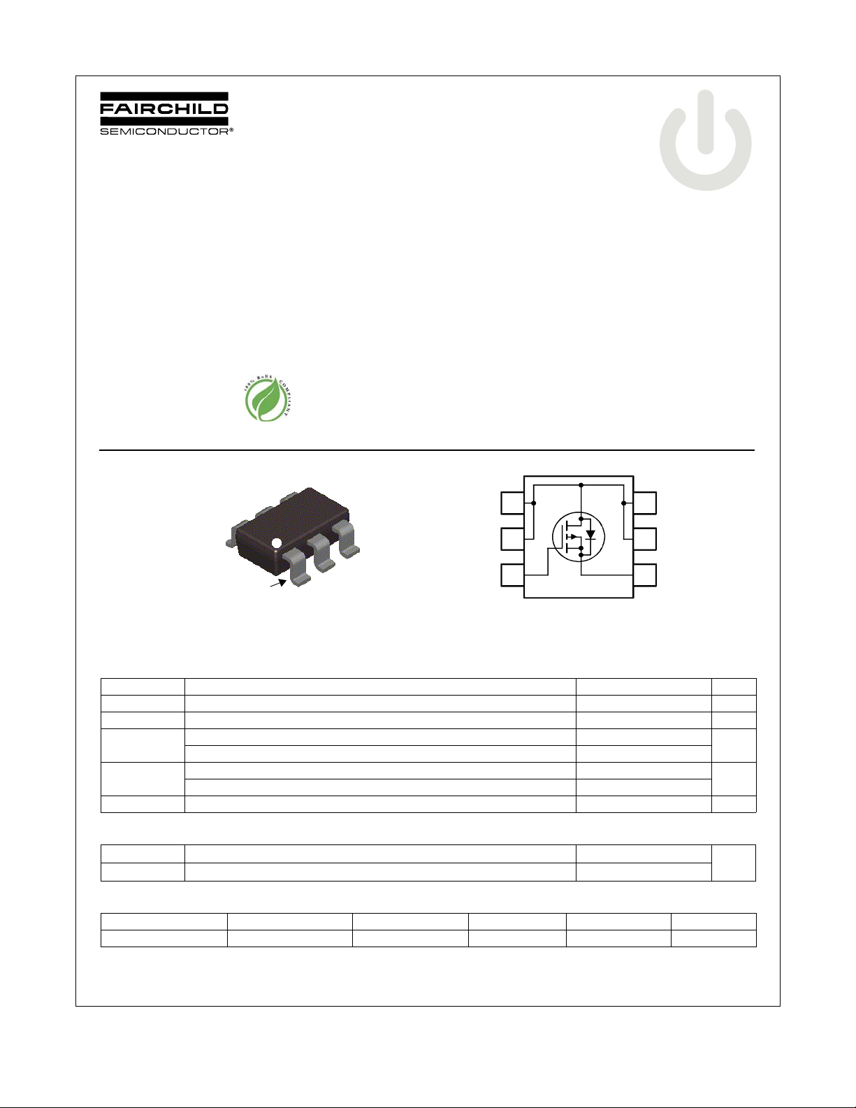
FDC365P
P-Channel PowerTrench® MOSFET
-35V, -4.3A, 55mΩ
Features
Max r
Max r
RoHS Compliant
= 55mΩ at VGS = -10V, ID = -4.2A
DS(on)
= 80mΩ at VGS = -4.5V, ID = -3.2A
DS(on)
General Description
This P-Channel MOSFET has been produced using Fairchild
Semiconductor’s proprietary PowerTrench
deliver low
superior performance benefit in the applications.
Applications
Inverter
Power Supplies
November 2007
®
technology to
r
and optimized Bvdss capability to offer
DS(on)
FDC365P P-Channel PowerTrench
®
MOSFET
S
D
D
G
Pin 1
SuperSOT
MOSFET Maximum Ratings T
Symbol Parameter Ratings Units
V
DS
V
GS
I
D
P
D
, T
T
J
STG
Drain to Source Voltage -35 V
Gate to Source Voltage ±20 V
-Continuous (Note 1a) -4.3
-Pulsed -20
Power Dissipation (Note 1a) 1.6
Power Dissipation (Note 1b) 0.8
Operating and Storage Junction Temperature Range -55 to +150 °C
D
D
TM
-6
= 25°C unless otherwise noted
C
1
D
D
2
G
3
D
6
5
D
S
4
Thermal Characteristics
R
θJA
R
θJA
Thermal Resistance, Junction to Ambient (Note 1a) 78
Thermal Resistance, Junction to Ambient (Note 1b) 156
Package Marking and Ordering Information
A
W
°C/W
Device Marking Device Package Reel Size Tape Width Quantity
.365P FDC365P SSOT6 7’’ 8mm 3000 units
©2007 Fairchild Semiconductor Corporation
FDC365P Rev.C
1
www.fairchildsemi.com
Page 2
FDC365P P-Channel PowerTrench
Electrical Characteristics T
= 25°C unless otherwise noted
J
Symbol Parameter Test Conditions Min Typ Max Units
Off Characteristics
BV
DSS
∆BV
DSS
∆T
J
I
DSS
I
GSS
On Characteristics
V
GS(th)
∆V
GS(th)
∆T
J
r
DS(on)
g
FS
Drain to Source Breakdown Voltage ID = -250µA, VGS = 0V -35 V
Breakdown Voltage Temperature
Coefficient
Zero Gate Voltage Drain Current VDS = -28V, V
Gate to Source Leakage Current VGS = ±20V, V
ID = -250µA, referenced to 25°C -26 mV/°C
= 0V -1 µA
GS
= 0V ±100 nA
DS
Gate to Source Threshold Voltage VGS = VDS, ID = -250µA -1 -1.8 -3 V
Gate to Source Threshold Voltage
Temperature Coefficient
Static Drain to Source On Resistance
Forward Transconductance VDS = -10V, ID = -4.2A 8.7 S
ID = -250µA, referenced to 25°C 5.0 mV/°C
VGS = -10V, ID = -4.2A 45 55
VGS = -10V , ID = -4.2A, TJ = 125°C 69 90
Dynamic Characteristics
C
iss
C
oss
C
rss
R
g
Input Capacitance
Output Capacitance 105 135 pF
Reverse Transfer Capacitance 55 80 pF
VDS = -20V, VGS = 0V,
f = 1MHz
530 705 pF
Gate Resistance f = 1MHz 6.1 Ω
Switching Characteristics
t
d(on)
t
r
t
d(off)
t
f
Q
Q
Q
Q
g
g
gs
gd
Turn-On Delay Time
Rise Time 3 10 ns
Turn-Off Delay Time 15 28 ns
VDD = -20V, ID = -4.2A,
VGS = -10V, R
GEN
= 6Ω
7 13 ns
Fall Time 3 10 ns
Total Gate Charge V
Total Gate Charge V
Gate to Source Charge 1.7 nC
= 0V to -10V
GS
= 0V to -5V 6 9 nC
GS
VDD = -20V,
ID = -4.2A
11 15 nC
Gate to Drain “Miller” Charge 2.2 nC
mΩVGS = -4.5V, ID = -3.2A 70 80
®
MOSFET
Drain-Source Diode Characteristics
V
SD
t
rr
Q
rr
Notes:
is the sum of the junction-to-case and case-to-ambient thermal resistance where the case thermal reference is defined as the solder mounting surface of the drain pins.
1: R
θJA
R
θJC
2: Pulse Test: Pulse Width < 300µs, Duty cycle < 2.0%.
©2007 Fairchild Semiconductor Corporation
FDC365P Rev.C
Source to Drain Diode Forward Voltage V
Reverse Recovery Time
Reverse Recovery Charge 7 14 nC
is guaranteed by design while R
is determined by the user’s board design.
θJA
GS
IF = -4.2A, di/dt = 100A/µs
a.
78°C/W when mounted on a 1
2
in
pad of 2 oz copper on FR-4
board.
= 0V, IS = -1.3A (Note 2) -0.8 -1.2 V
16 29 ns
b.
156°C/W when mounted on a
minimum pad of 2 oz copper.
2
www.fairchildsemi.com
Page 3

FDC365P P-Channel PowerTrench
Typical Characteristics T
20
16
12
8
, DRAIN CURRENT (A)
D
-I
4
0
012345
Figure 1.
1.6
1.4
1.2
1.0
NORMALIZED
0.8
DRAIN TO SOURCE ON-RESISTANCE
0.6
-75 -50 -25 0 25 50 75 100 125 150
Figu r e 3. Nor m a lized O n - Resist a n ce
VGS = -10V
VGS = -4.5V
PULSE DURATION = 80µs
DUTY CYCLE = 0.5%MAX
-VDS, DRAIN TO SOURCE VOLTAGE (V)
On-Region Characteristics Figure 2.
ID = - 4.2A
V
= -10V
GS
T
, JUNCTION TEMPERATURE (
J
vs Junction Temperature
= 25°C unless otherwise noted
J
VGS = -4V
VGS = -3.5V
VGS = -3V
o
C)
4.0
3.5
3.0
VGS = -3V
PULSE DURATION = 80µs
DUTY CYCLE = 0.5%MAX
VGS = -3.5V
2.5
VGS = -4V
VGS = -4.5V
V
= -10V
GS
2.0
NORMALIZED
1.5
1.0
DRAIN TO SOURCE ON-RESISTANCE
0.5
048121620
-ID, DRAIN CURRENT(A)
Norma l i z e d O n - Resistance
vs Drain Current and Gate Voltage
200
ID = -4.2A
160
(mΩ)
120
, DRAIN TO
80
DS(on)
r
40
SOURCE ON-RESISTANCE
0
246810
-VGS, GATE TO SOURCE VOLTAG E (V)
Figure 4.
On-Resistanc e vs Gate to
PULSE DURATION = 80µs
DUTY CYCLE = 0.5%MAX
TJ = 125oC
o
T
= 25
C
J
Source Voltage
®
MOSFET
20
PULSE DURATION = 80µs
DUTY CYCLE = 0.5%MAX
16
V
= -5V
DS
12
8
, DRAIN CURRENT (A)
D
4
-I
0
12345
TJ = 150oC
TJ = 25oC
-VGS, GATE TO SOURCE V OLTAGE (V)
Figure 5. Transfer Characteristics
©2007 Fairchild Semiconductor Corporation
FDC365P Rev.C
TJ = -55oC
20
V
= 0V
GS
TJ = 150oC
TJ = 25oC
TJ = -55oC
0.0 0.2 0.4 0.6 0.8 1.0 1.2
-VSD, BODY DIODE FORWARD VOLTAGE (V)
Figure 6.
Source to Dr ai n Diode
0.1
0.01
, REVERSE DRAIN CURRENT (A)
S
-I
0.001
10
1
Forward Voltage vs Source Current
3
www.fairchildsemi.com
Page 4

FDC365P P-Channel PowerTrench
Typical Characteristics T
10
ID = -4.2A
8
VDD = -20V
6
V
= -15V
4
2
, GATE TO SOURCE VOLTAGE(V)
GS
-V
0
036912
Figure 7.
30
10
1
THIS AREA IS
LIMITED BY r
0.1
, DRAIN CURRENT (A)
D
-I
0.01
0.1 1 10 100
Figure 9.
DD
Qg, GATE CHARGE(nC)
Gate Charge Characteristics Figure 8.
DS(on)
SINGLE PULSE
T
= MAX RATED
J
o
= 156
θJA
C/W
o
C
R
TA = 25
-VDS, DRAIN to SOURCE VOLTAGE (V)
Forward Bias Safe
Operating Area
= 25°C unless otherwise noted
J
VDD = -25V
0.1ms
1ms
10ms
100ms
1s
10s
DC
1000
100
CAPACITANCE (pF)
30
0.1 1 10
400
100
10
), PEAK TRANSIENT POWER (W)
1
PK
P(
0.5
10-410-310-210
Figure 10.
C
iss
C
oss
f = 1MHz
V
= 0V
GS
C
rss
35
-VDS, DRAIN TO SOURCE VOLTAGE (V)
Capacitance vs Drain
to Source Voltage
-1
SINGLE PULSE
R
= 156oC/W
θJA
T
= 25oC
A
110
100 1000
VGS = -10V
t, PULSE WIDTH (s)
Single Pulse Maximum Power Dissipation
®
MOSFET
2
1
DUTY CYCLE-DESCENDING ORDER
D = 0.5
0.1
0.2
0.1
0.05
0.02
0.01
-4
10
10
θJA
IMPEDANCE, Z
0.01
NORMALIZED THERMAL
0.001
©2007 Fairchild Semiconductor Corporation
FDC365P Rev.C
SINGLE PULSE
R
-3
θJA
= 156
o
C/W
-2
10
t, RECTANGULAR PULSE DURATION (sec)
-1
10
110
Figure 11. Transient Thermal Response Curve
4
NOTES:
DUTY FACTOR: D = t
PEAK TJ = PDM x Z
P
DM
t
1
t
2
1/t2
x R
+ T
θJA
θJA
A
100 1000
www.fairchildsemi.com
Page 5

Dimensional Outline and Pad Layout
FDC365P P-Channel PowerTrench
®
MOSFET
©2007 Fairchild Semiconductor Corporation
FDC365P Rev.C
5
www.fairchildsemi.com
Page 6

Preliminary Datasheet
®
TRADEMARKS
The following are registered and unregistered trademarks and service marks Fairchild Semiconductor owns or is authorized to use and
is not intended to be an exhaustive list of all such trademarks.
®
ACEx
Build it Now™
CorePLUS™
CROSSVOLT™
CTL™
Current Transfer Logic™
EcoSPARK
Fairchild
®
®
Fairchild Semiconductor
FACT Quiet Series™
®
FACT
®
FAST
FastvCore™
FPS™
®
FRFET
Global Power Resource
Green FPS™
Green FPS™ e-Series™
GTO™
i-Lo™
IntelliMAX™
ISOPLANAR™
MegaBuck™
MICROCOUPLER™
®
MicroFET™
MicroPak™
MillerDrive™
Motion-SPM™
OPTOLOGIC
OPTOPLANAR
®
SM
PDP-SPM™
Power220
®
®
®
Power247
POWEREDGE
Power-SPM™
PowerTrench
Programmable Active Droop™
QFET
QS™
QT Optoelectronics™
Quiet Series™
RapidConfigure™
SMART START™
SPM
STEALTH™
SuperFET™
SuperSOT™-3
SuperSOT™-6
®
®
®
®
SuperSOT™-8
SyncFET™
The Power Franchise
TinyBoost™
TinyBuck™
TinyLogic
®
®
TINYOPTO™
TinyPower™
®
TinyPWM™
TinyWire™
µSerDes™
®
UHC
UniFET™
VCX™
FDC365P P-Channel PowerTrench
®
MOSFET
DISCLAIMER
FAIRCHILD SEMICONDUCTOR RESERVES THE RIGHT TO MAKE CHANGES WITHOUT FURTHER NOTICE TO ANY PRODUCTS
HEREIN TO IMPROVE RELIABILITY, FUNCTION, OR DESIGN. FAIRCHILD DOES NOT ASSUME ANY LIABILITY ARISING OUT OF
THE APPLICATION OR USE OF ANY PRODUCT OR CIRCUIT DESCRIBED HEREIN; NEITHER DOES IT CONVEY ANY LICENSE
UNDER ITS PATENT RIGHTS, NOR THE RIGHTS OF OTHERS. THESE SPECIFICATIONS DO NOT EXPAND THE TERMS OF
FAIRCHILD’S WORLDWIDE TERMS AND CONDITIONS, SPECIFICALLY THE WARRANTY THEREIN, WHICH COVERS THESE
PRODUCTS.
LIFE SUPPORT POLICY
FAIRCHILD’S PRODUCTS ARE NOT AUTHORIZED FOR USE AS CRITICAL COMPONENTS IN LIFE SUPPORT DEVICES OR
SYSTEMS WITHOUT THE EXPRESS WRITTEN APPROVAL OF FAIRCHILD SEMICONDUCTOR CORPORATION.
As used herein:
1. Life support devices or systems are devices or systems
which, (a) are intended for surgical implant into the body or
(b) support or sustain life, and (c) whose failure to perform
when properly used in accordance with instructions for use
2. A critical component in any component of a life support,
device, or system whose failure to perform can be
reasonably expected to cause the failure of the life support
device or system, or to affect its safety or effectiveness.
provided in the labeling, can be reasonably expected to
result in a significant injury to the user.
PRODUCT STATUS DEFINITIONS
Definition of Terms
Datasheet Identification Product Status Definition
Advance Information Formative or In Design
This datasheet contains the design specifications for product
development. Specifications may change in any manner without notice.
This datasheet contains preliminary data; supplementary data will be pub-
Preliminary First Production
lished at a later date. Fairchild Semiconductor reserves the right to make
changes at any time without notice to improve design.
No Identification Needed Full Production
This datasheet contains final specifications. Fairchild Semiconductor reserves
the right to make changes at any time without notice to improve design.
This datasheet contains specifications on a product that has been discontin-
Obsolete Not In Production
ued by Fairchild Semiconductor. The datasheet is printed for reference information only.
©2007 Fairchild Semiconductor Corporation
FDC365P Rev.C
6
www.fairchildsemi.com
Rev. I31
 Loading...