

Page 1
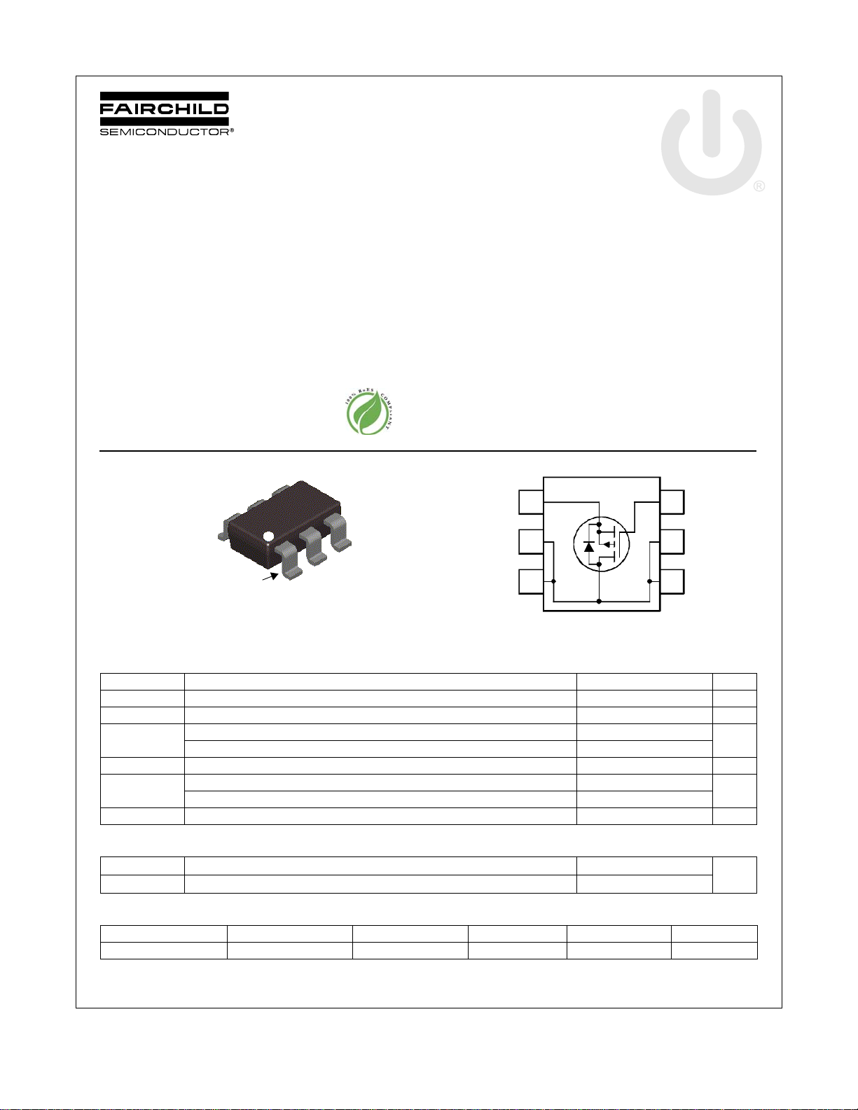
FDC3535
SuperSOTTM -6
G
S
D
D
D
D
Pin 1
1
2
3
6
5
4
D
D
G
D
D
S
P-Channel Power Trench® MOSFET
-80 V, -2.1 A, 183 mΩ
Features
Max r
Max r
High performance trench technology for extremely low r
High power and current handling capability in a widely used
surface mount package
Fast switching speed
100% UIL Tested
RoHS Compliant
= 183 mΩ at VGS = -10 V, ID = -2.1 A
DS(on)
= 233 mΩ at VGS = -4.5 V, ID = -1.9 A
DS(on)
DS(on)
General Description
This P-Channel MOSFET is produced using Fairchild
Semiconductor‘s advanced Power Trench
been optimized for r
ruggedness.
Applications
Load Switch
Synchronous Rectifier
June 2010
®
, switching performance and
DS(on)
process that has
FDC3535 P-Channel Power Trench
®
MOSFET
MOSFET Maximum Ratings T
Symbol Parameter Ratings Units
V
DS
V
GS
I
D
E
AS
P
D
, T
T
J
STG
Thermal Characteristics
R
θJC
R
θJA
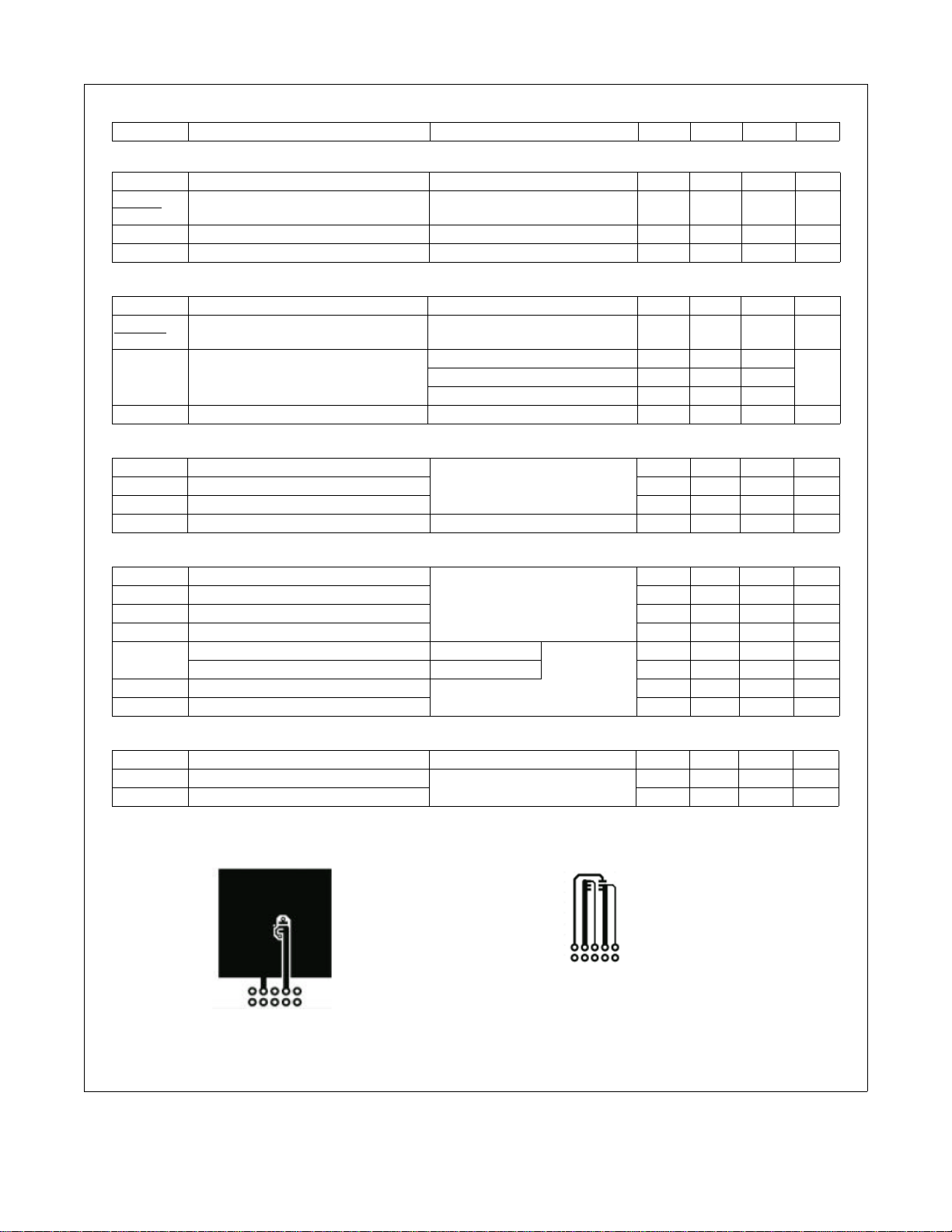
Package Marking and Ordering Information
Device Marking Device Package Reel Size Tape Width Quantity
©2010 Fairchild Semiconductor Corporation
FDC3535 Rev. C
Drain to Source Voltage -80 V
Gate to Source Voltage ±20 V
Drain Current -Continuous (Note 1a) -2.1
-Pulsed -10
Single Pulse Avalanche Energy (Note 3) 37 mJ
Power Dissipation (Note 1a) 1.6
Power Dissipation (Note 1b) 0.7
Operating and Storage Junction Temperature Range -55 to +150 °C
Thermal Resistance, Junction to Case 30
Thermal Resistance, Junction to Ambient (Note 1a) 78
.535 FDC3535 SSOT-6 7 ’’ 8 mm 3000 units
= 25 °C unless otherwise noted
A
1
A
W
°C/W
www.fairchildsemi.com
Page 2
FDC3535 P-Channel Power Trench
Electrical Characteristics T
= 25 °C unless otherwise noted
J
Symbol Parameter Test Conditions Min Typ Max Units
Off Characteristics
BV
ΔBV
ΔT
I
DSS
I
GSS
DSS
DSS
J
Drain to Source Breakdown Voltage ID = -250 μA, VGS = 0 V -80 V
Breakdown Voltage Temperature
Coefficient
Zero Gate Voltage Drain Current VDS = -64 V, V
Gate to Source Leakage Current VGS = ±20 V, V
I
= -250 μA, referenced to 25 °C -64 mV/°C
D
= 0 V -1 μA
GS
= 0 V ±100 nA
DS
On Characteristics
V
GS(th)
ΔV
ΔT
r
DS(on)
g
FS
GS(th)
J
Gate to Source Threshold Voltage VGS = VDS, ID = -250 μA-1-1.6-3V
Gate to Source Threshold Voltage
Temperature Coefficient
Static Drain to Source On Resistance
I
= -250 μA, referenced to 25 °C 5 mV/°C
D
V
= -10 V, ID = -2.1 A 147 183
GS
= -4.5 V, ID = -1.9 A 176 233
GS
= -10 V, ID = -2.1 A, TJ = 125 °C 246 307
V
GS
Forward Transconductance VDD = -10 V, ID = -2.1 A 6.3 S
Dynamic Characteristics
C
iss
C
oss
C
rss
R
g
Input Capacitance
Output Capacitance 49 65 pF
Reverse Transfer Capacitance 24 40 pF
= -40 V, VGS = 0 V,
V
DS
f = 1 MHz
Gate Resistance 5.7 Ω
659 880 pF
Switching Characteristics
t
d(on)
t
r
t
d(off)
t
f
Q
g(TOT)
Q
gs
Q
gd
Turn-On Delay Time
Rise Time 3.1 10 ns
Turn-Off Delay Time 23 38 ns
= -40 V, ID = -2.1 A,
V
DD
V
= -10 V, R
GS
GEN
= 6 Ω
Fall Time 2.9 10 ns
Total Gate Charge VGS = 0 V to -10 V
Total Gate Charge V
Total Gate Charge 1.6 nC
= 0 V to -4.5 V 6.8 10 nC
GS
= -40 V
V
DD
I
= -2.1 A
D
Gate to Drain “Miller” Charge 2.7 nC
6.5 13 ns
14 20 nC
mΩV
®
MOSFET
Drain-Source Diode Characteristics
V
SD
t
rr
Q
rr
NOTES:
1. R
is the sum of the junction-to-case and case-to-ambient thermal resistance where the case thermal reference is defined as the solder mounting surface of the drain pins.
θJA
R
is guaranteed by design while R
θJC
2. Pulse Test: Pulse Width < 300 μs, Duty cycle < 2.0 %.
3. Starting T
©2010 Fairchild Semiconductor Corporation
FDC3535 Rev. C
Source to Drain Diode Forward Voltage V
Reverse Recovery Time
Reverse Recovery Charge 23 38 nC
is determined by the user's board design.
θCA
= 25 oC, L = 3 mH, IAS = -5 A, VDD = -80 V, VGS = -10 V.
J
= 0 V, IS = -2.1 A (Note 2) -0.81 -1.3 V
GS
= -2.1 A, di/dt = 100 A/μs
I
F
a. 78 °C/W when mounted on
2
pad of 2 oz copper
a 1 in
2
25 40 ns
b.175 °C/W when mounted on
a minimum pad of 2 oz copper
www.fairchildsemi.com
Page 3
FDC3535 P-Channel Power Trench
012345
0
2
4
6
8
10
VGS = -3.5 V
VGS = -10 V
VGS = -2.5 V
VGS = -3 V
VGS = -4.5 V
PULSE DURATION = 80 μs
DUTY CYCLE = 0.5% MAX
-I
D
, DRAIN CURRENT (A)
-VDS, DRA IN TO SOURCE VOLTAGE (V)
0246810
0
1
2
3
4
VGS = -3.5 V
VGS = -2.5 V
PULSE DURATION = 80 μs
DUTY CYCLE = 0.5% MAX
NORMALIZED
DRAIN TO SOURCE ON-RESISTANCE
-ID, DRAIN CURRENT (A)
VGS = -4.5 V
VGS = -3 V
V
GS
= -10 V
-75 -50 -25 0 25 50 75 100 125 150
0.4
0.6
0.8
1.0
1.2
1.4
1.6
1.8
2.0
ID = - 2.1 A
V
GS
= -10 V
NORMALIZED
DRAIN TO SOURCE ON-RESIST ANCE
T
J
, JUNCTION TEMPERATURE (
o
C)
246810
100
200
300
400
500
600
PULSE DURATION = 80 μs
DUTY CYCLE = 0.5% MAX
TJ = 125 oC
T
J
= 25
o
C
ID = -2.1 A
r
DS(on)
, DRAIN TO
SOURCE ON-RESISTANCE
(mΩ)
-VGS, GATE TO S OURCE VOLTAGE ( V )
12345
0
2
4
6
8
10
TJ = 25 oC
V
DS
= -5 V
PULSE DURATION = 80 μs
DUTY CYCLE = 0.5% MAX
TJ = -55 oC
TJ = 150 oC
-I
D
, DRAIN CURRENT (A)
-VGS, GATE TO SOURCE VO LTAGE (V)
0.0 0.2 0.4 0.6 0.8 1.0 1.2
0.001
0.01
0.1
1
10
20
TJ = -55 oC
TJ = 25 oC
TJ = 150 oC
V
GS
= 0 V
-I
S
, REVERSE DRAIN CURRENT (A)
-VSD, BODY DIODE FORWARD VOLTAGE (V)
Typical Characteristics T
Figure 1.
On-Region Characteristics Figure 2.
= 25 °C unless otherwise noted
J
®
MOSFET
Normali z e d O n - R esistance
vs Drain Current and Gate Voltage
Figu r e 3. Norm a l ized On - R esista n c e
vs Junction Temperature
©2010 Fairchild Semiconductor Corporation
FDC3535 Rev. C
Figure 5. Transfer Characteristics
Figure 4.
On-Res istance vs Gate to
Source Voltage
Figure 6.
Source to Drain Diode
Forward Voltage vs Source Current
3
www.fairchildsemi.com
Page 4

FDC3535 P-Channel Power Trench
0 3 6 9 12 15
0
2
4
6
8
10
ID = -2.1 A
VDD = -50 V
V
DD
= -30 V
-V
GS
, GATE TO SOURCE VOLTAGE (V)
Qg, GATE CHARGE (nC)
VDD = -40 V
0.1 1 10 100
10
100
1000
f = 1 MHz
V
GS
= 0 V
CAPACITANCE (pF)
-VDS, DRAIN TO SOURCE VOLTAGE (V)
C
rss
C
oss
C
iss
0.01 0.1 1 10
1
2
3
4
5
6
7
TJ = 100 oC
TJ = 25 oC
TJ = 125 oC
tAV, TIME IN AVALANCHE (ms )
-I
AS
, AVALANCHE CURRENT (A)
25 50 75 100 125 150
0.0
0.5
1.0
1.5
2.0
2.5
R
θJA
= 78 oC/W
V
GS
= -4.5 V
V
GS
= -10 V
-I
D
, DRAIN CURRENT (A)
T
C
, Ambient TEMPERATURE (
o
C)
0.1 1 10 100 300
0.005
0.01
0.1
1
10
20
THIS AR E A IS
LIMITED BY r
DS(on)
100 us
1 ms
100 ms
1 s
DC
10 s
10 ms
SINGLE PULSE
T
J
= MAX RATED
R
θJA
= 175
o
C/W
TA = 25
o
C
-I
D
, DRAIN CURRENT (A)
-VDS, DRAIN to SOURCE VOLTAGE (V)
10-410-310-210-1110
100 1000
0.5
1
10
100
1000
SINGLE PULSE
R
θJA
= 175 oC/W
T
A
= 25 oC
VGS = -10 V
P(
PK
), PEAK TRANSIENT POWER (W)
t, PULSE WIDTH (s)
Typical Characteristics T
Figure 7.
Gate Charge Characteristics Figure 8.
= 25 °C unless otherwise noted
J
Capacitance vs Drain
to Source Voltage
®
MOSFET
Figure 9.
Uncl a m p e d I n duct i v e
Switching Capability
Figure 11.
Operating Area
©2010 Fairchild Semiconductor Corporation
FDC3535 Rev. C
Forward Bias Safe
Figure 10.
Max i mum C o ntin u ous Dra i n
Current vs Ambient Temperature
Fi gur e 12 . Si ngl e Pu lse Max imu m
Power Dissipation
4
www.fairchildsemi.com
Page 5

FDC3535 P-Channel Power Trench
10
-4
10
-3
10
-2
10
-1
110
100 1000
0.001
0.01
0.1
1
2
SINGLE PULSE
R
θJA
= 175 oC/W
DUTY CYCLE-DESCENDING ORDER
NORMALIZED THERMAL
IMPEDANCE,
Z
θJA
t, RECTANGULAR PU L SE DURATION (sec)
D = 0.5
0.2
0.1
0.05
0.02
0.01
P
DM
t
1
t
2
NOTES:
DUTY FACTOR: D = t
1/t2
PEAK TJ = PDM x Z
θJA
x R
θJA
+ T
A
Typical Characteristics T
Figure 13. Junction-to-Ambient Transient Thermal Response Curve
= 25 °C unless otherwise noted
J
®
MOSFET
©2010 Fairchild Semiconductor Corporation
FDC3535 Rev. C
5
www.fairchildsemi.com
Page 6
FDC3535 P-Channel Power Trench
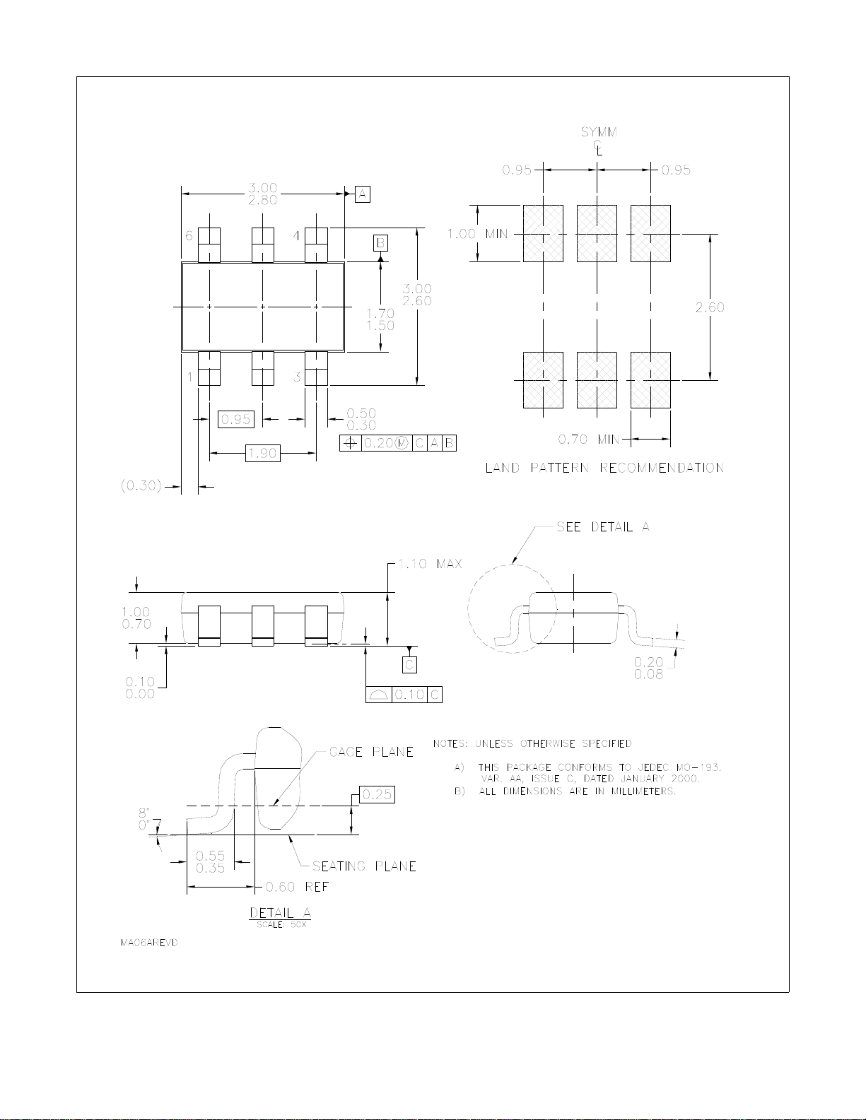
Dimensional Outline and Pad Layout
®
MOSFET
©2010 Fairchild Semiconductor Corporation
FDC3535 Rev. C
6
www.fairchildsemi.com
Page 7
TRADEMARKS
tm
®
tm
The following includes registered and unregistered trademarks a nd service marks, owned by Fairch ild Semiconduct or and/or its global sub sidiaries, and is not
intended to be an exhaustive list of all such trademarks.
AccuPower™
Auto-SPM™
Build it Now™
CorePLUS™
CorePOWER™
CROSSVOLT™
CTL™
Current Transfer Logic™
DEUXPEED
Dual Cool™
EcoSPARK
EfficentMax™
ESBC™
Fairchild
Fairchild Semiconductor
FACT Quiet Series™
FACT
FAST
FastvCore™
FETBench™
FlashWriter
FPS™
®
®
®
®
®
®
*
F-PFS™
®
FRFET
Global Power Resource
Green FPS™
Green FPS™ e-Series™
Gmax™
GTO™
IntelliMAX™
ISOPLANAR™
MegaBuck™
MICROCOUPLER™
MicroFET™
MicroPak™
MicroPak2™
MillerDrive™
®
MotionMax™
Motion-SPM™
OptiHiT™
OPTOLOGIC
OPTOPLANAR
®
®
SM
®
PDP SPM™
Power-SPM™
PowerTrench
PowerXS™
Programmable Active Droop™
QFET
QS™
Quiet Series™
RapidConfigure™
®
®
™
Saving our world, 1mW/W/kW at a time™
SignalWise™
SmartMax™
SMART START™
®
SPM
STEALTH™
SuperFET™
SuperSOT™-3
SuperSOT™-6
SuperSOT™-8
SupreMOS™
SyncFET™
Sync-Lock™
®*
The Power Franchise
®
TinyBoost™
TinyBuck™
TinyCalc™
®
TinyLogic
TINYOPTO™
TinyPower™
TinyPWM™
TinyWire™
TriFault Detect™
TRUECURRENT™*
μSerDes™
®
UHC
Ultra FRFET™
UniFET™
VCX™
VisualMax™
XS™
®
*Trademarks of System General Corporation, used under license by Fairchild Semiconductor.
DISCLAIMER
FAIRCHILD SEMICONDUCTOR RESERVES THE RIGHT TO MAKE CHANGES WITHOUT FURTHER NOTICE TO ANY PRODUCTS HEREIN TO IMPROVE
RELIABILITY, FUNCTION, OR DESIGN. FAIRCHILD DOES NOT ASSUME ANY LIABILITY ARISING OUT OF THE APPLICATION OR USE OF ANY
PRODUCT OR CIRCUIT DESCRIBED HEREIN; NEITHER DOES IT CONVEY ANY LICENSE UNDER ITS PATENT RIGHTS, NOR THE RIGHTS OF OTHERS.
THESE SPECIFICATIONS DO NOT EXPAND THE TERMS OF FAIRCHILD’S WORLDWIDE TERMS AND CONDITIONS, SPECIFICALLY THE WARRANTY
THEREIN, WHICH COVERS THESE PRODUCTS.
FDC3535 P-Channel Power Trench
®
MOSFET
LIFE SUPPORT POLICY
FAIRCHILD’S PRODUCTS ARE NOT AUTHORIZED FOR USE AS CRITICAL COMPONENTS IN LIFE SUPPORT DEVICES OR SYSTEMS WITHOUT THE
EXPRESS WRITTEN APPROVAL OF FAIRCHILD SEMICONDUCTOR CORPORATION.
As used here in:
1. Life support devices or systems are devices or systems which, (a) are
intended for surgical implant into the body or (b) support or sustain life,
and (c) whose failure to perform when properly used in accordance with
instructions for use provided in the labeling, can be reasonably
2. A critical component in any component of a life support, device, or
system whose failure to perform can be reasonably expected to cause
the failure of the life support device or system, or to affect its safety or
effectiveness.
expected to result in a significant injury of the user.
ANTI-COUNTERFEITING POLICY
Fairchild Semiconductor Corporation’s Anti-Counterfeiting Policy. Fairchild’s Anti-Counterfeiting Policy is also stated on our external website,
www.Fairchildsemi.com, under Sales Support
Counterfeiting of semiconductor parts is a growing problem in the indust ry. All manufactures of semiconductor products are experiencin g counterfeiting of their
parts. Customers who inadvertently purchase counte rfe it parts e xpe rien ce many probl ems such as loss of b rand reputa tio n, subst andard p erf orman ce, fai led
application, and increased cost of production and manufacturing del ays. Fairch ild is taking stro ng measure s to prot ect ourselves and our customers fro m the
proliferation of counterfeit parts. Fairchild strongly encou rages customer s to purchase Fairchild parts either direct ly from Fairchild or from Authorized Fairchild
Distributors who are listed by country on our web page cited above. Products customers buy either from Fairchild directly or from Authorized Fairchild
Distributors are genuine parts, have full traceability, meet Fairchild’s qua lity standards for handing and storage and provide access to Fairchild’s full range o f
up-to-date technical and product information. Fairchild and our Authorized Distributors will stand behind all warranties and will appropriately address and
warranty issues that may arise. Fairchild will not provide any warranty coverage or other assistance for parts bought from Unauthorized Sources. Fairchild is
committed to combat this global problem and encourage our customer s to do their part in stopping this practice by buying direct or from authorized distrib utors.
PRODUCT STATUS DEFINITIONS
Definition of Terms
.
Datasheet Identification Product Status Definition
Advance Information Formative / In Design
Preliminary First Production
No Identification Needed Full Production
Obsolete Not In Production
©2010 Fairchild Semiconductor Corporation
FDC3535 Rev. C
Datasheet contains the design specifications for product development. Specifications
may change in any manner without notice.
Datasheet contains preliminary data; supplementary data will be published at a later
date. Fairchild Semiconductor reserves the right to make changes at any time without
notice to improve design.
Datasheet contains final specifications. Fairchild Semiconductor reserves the right to
make changes at any time without notice to improve the design.
Datasheet contains specifications on a product that is discontinu ed by Fairchild
Semiconductor. The datasheet is for reference information only.
7
www.fairchildsemi.com
Rev. I48
 Loading...