

Page 1
SANYO Electric Co.,Ltd. Semiconductor Bussiness Headquaters
TOKYO OFFICE Tokyo Bldg., 1-10, 1 Chome, Ueno, Taito-ku, TOKYO, 110-8534 JAPAN
N-Channel Junction Silicon FET
Low-Frequency General-Purpose Amp,
Differential Amp Applications
Ordering number:EN3154
FC11
Features
· Adoption of FBET process.
· Composite type with 2 transistors contained in the
CP package currently in use, improving the mounting efficiency greatly.
· The FC11 is formed with two chips, being equivalent
to the 2SK771, placed in one package.
· Excellent in the thermal equilibrium and pair capability and suitable for use in differential amp.
· Common source.
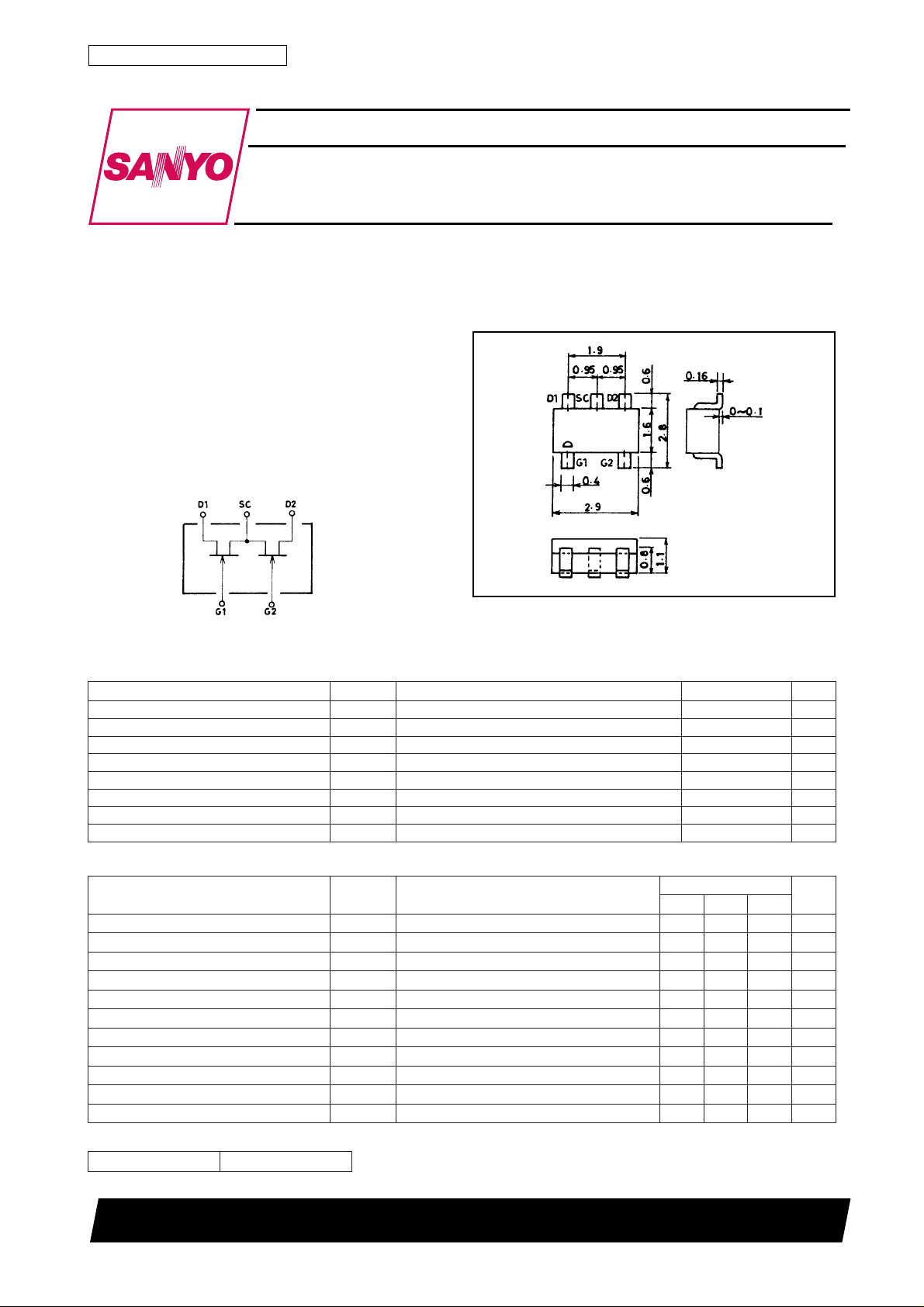
Electrical Connection
Specifications
Absolute Maximum Ratings at Ta = 25˚C
retemaraPlobmySsnoitidnoCsgnitaRtinU
egatloVecruoS-ot-niarDV
egatloVniarD-ot-etaGV
tnerruCetaGI
tnerruCniarDI
noitapissiDrewoPelbawollA
noitapissiDlatoTP
erutarepmeTnoitcnuJjT 051
erutarepmeTegarotSgtsT 051+ot55–
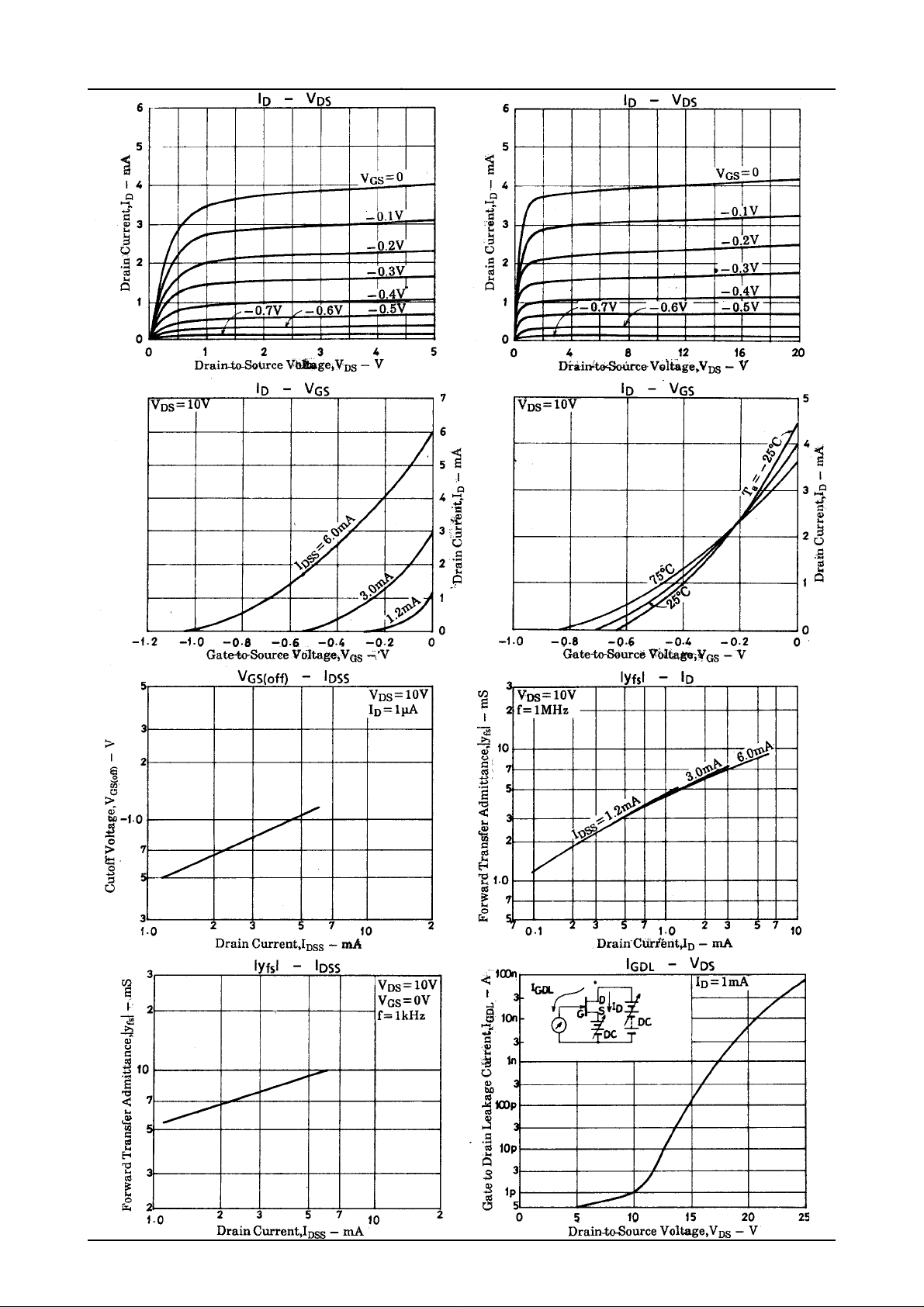
Electrical Characteristics at Ta = 25˚C
retemaraPlobmySsnoitidnoC
egatloVnwodkaerBniarD-ot-etaGV
tnerruCffotuCetaGI
egatloVffotuCV
porDegatloVecruoS-ot-etaG
tnerruCniarDI
oitaRtnerruCniarDV
ecnattimdArefsnarTdrawroFY|sf|VSDV,V01=
oitaRecnattimdArefsnarTdrawroFV
ecncaticapaCtupnIssiCVSDV,V01=
ecnaticapaCrefsnarTesreveRssrCVSDV,V01=
erugiFesioNFNVSDR,V01=
Note*:The FC11 is classified by I
0.3D2.10.6E5.2
as follows (unit:mA)
DSS
∆V
XSD
SDG
G
D
P
D
T
I
SDG)RB(
G
V
SSG
V
)ffo(SG
V|
SG
V
SSD
Package Dimensions
unit:mm
2070
[FC11]
G1:Gate1
G2:Gate2
D2:Drain2
SC:Source Common
D1:Drain1
SANYO:CP5
04V
04–V
01Am
01Am
tinu1 002Wm
003Wm
sgnitaR
nimpytxam
V,Aµ01=
0=04–V
SD
V,V02–=
SG
SD
SG
SD
SD
SD
V0=0.1–An
SD
I,V01=
Aµ1=3.0–9.0–8.1–V
D
V–egral
SG
V,V01=
SG
I,V01=
SSD
SG
Y|,V01=
sf
SG
SG
k1= Ω I,
g
V,|llams
V0=*2.1*0.6Am
I/llams
SSD
zHk1=f,V0=5.40.9Sm
Y|/llams|
sf
zHM1=f,V0=0.9Fp
zHM1=f,V0=1.2Fp
D
I,V01=
SD
egral9.0
egral|9.0
Am1=03Vm
D
zHk1=f,Am1=5.1Bd
Marking:11
I
rank:D,E
DSS
The Specifications shown above are for each individual
transistor.
˚C
˚C
tinU
52098HA (KT)/7259TA, TS No.3154-1/3
Page 2
FC11
No.3154-2/3
Page 3

FC11
No products described or contained herein are intended for use in surgical implants, life-support systems,
aerospace equipment, nuclear power control systems, vehicles, disaster/crime-prevention equipment and
the like, the failure of which may directly or indirectly cause injury, death or property loss.
Anyone purchasing any products described or contained herein for an above-mentioned use shall:
Accept full responsibility and indemnify and defend SANYO ELECTRIC CO., LTD., its affiliates,
subsidiaries and distributors and all their officers and employees, jointly and severally, against any
and all claims and litigation and all damages, cost and expenses associated with such use:
Not impose any responsibilty for any fault or negligence which may be cited in any such claim or
litigation on SANYO ELECTRIC CO., LTD., its affiliates, subsidiaries and distributors or any of
their officers and employees jointly or severally.
Information (including circuit diagrams and circuit parameters) herein is for example only; it is not guaranteed for volume production. SANYO believes information herein is accurate and reliable, but no guarantees
are made or implied regarding its use or any infringements of intellectual property rights or other rights of
third parties.
This catalog provides information as of May, 1998. Specifications and information herein are subject to
change without notice.
PS No.3154-3/3
 Loading...