

Page 1
FAN7314 LCD Backlight Inverter Drive IC
March 2006
FAN7314
LCD Backlight Inverter Drive IC
Features
High-efficiency single-stage power conversion
■
■
Wide input voltage range: 5V to 25.5V
Back light lamp ballast and soft dimming
■
■
Reduces number of required external components
Precision voltage reference trimmed to 2%
■
■
ZVS half-bridge topology
■
Soft start
PWM control at fixed frequency
■
■
Analog and burst dimming function
Programmable striking frequency
■
■
Open lamp protection
Open lamp regulation
■
■
20-Pin SOIC
Description
The FAN7314 provides all the control functions for use
as a series parallel resonant converter as well as a pulse
width modulation (PWM) controller to develop a supply
voltage. Typical operating frequency range is between
30kHz and 250kHz, depending on the CCFL and the
transformer’s characteristics.
Ordering Information
Product number Package Operating Temperature
FAN7314M 20-SOIC -25°C to 85°C
FAN7314MX
FPS™ is a trademark of Fairchild Semiconductor Corporation.
©2006 Fairchild Semiconductor Corporation
FAN7314 Rev. 1.0.1
1
www.fairchildsemi.com
Page 2
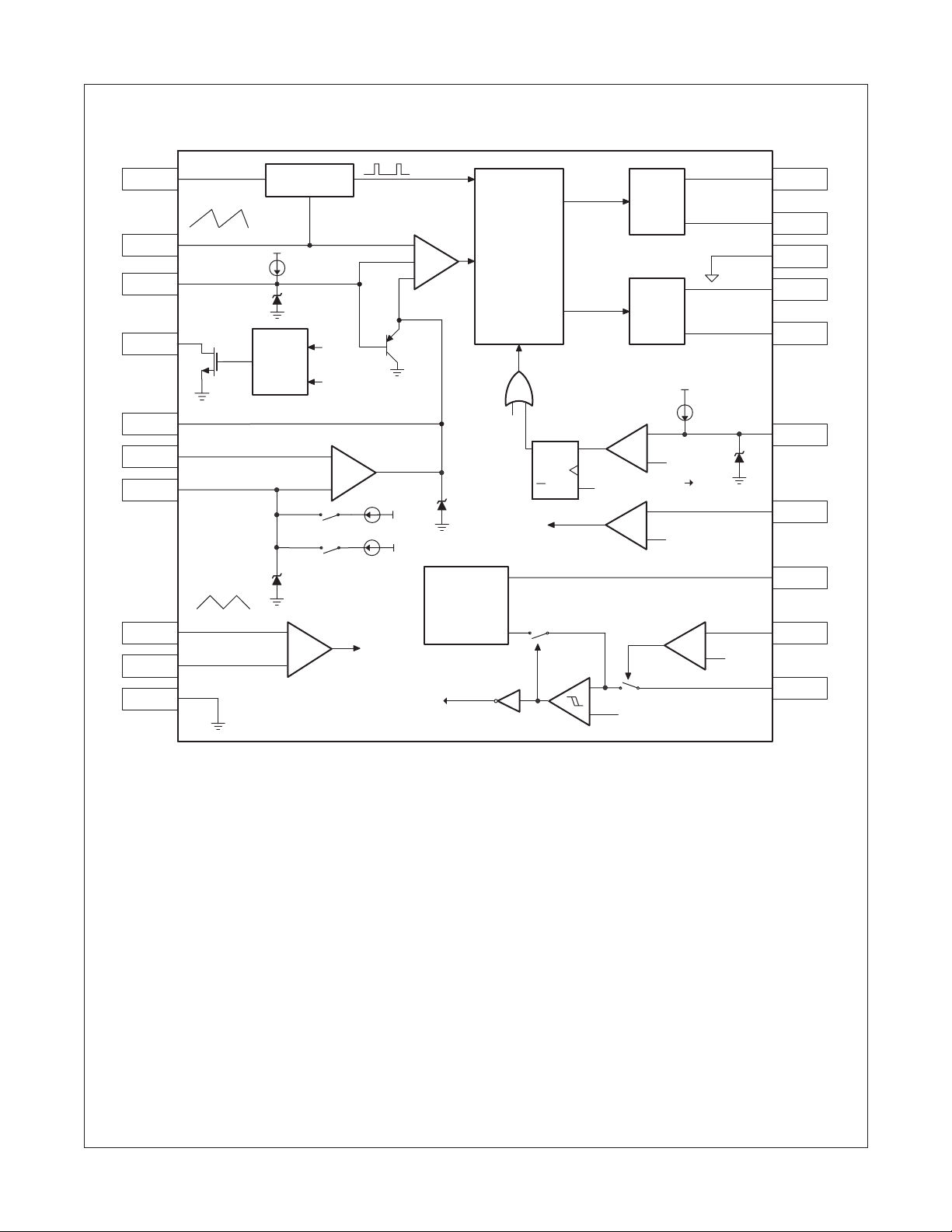
Internal Block Diagram
FAN7314 LCD Backlight Inverter Drive IC
RT
CT
S_S
RT1
EA_OUT
ADIM
EA_IN
BCT
BDIM
AGND
max. 2V
min. 0.5V
M
RT1
max. 2V
min. 0.5V
6µA
Oscillator
Striking
Logic
Va+α
2.65V
OLP
S_S
+
–
Solr 105µA
Sburst 85µA
–
+
Error Amp.
Sburst
UVLO
–
+
+
2.5V
Voltage
Reference
Internal Bias
OUTA
Output
Driver
OUTB
Output
Control
PGND
Logic
OUTC
Output
Driver
OUTD
1.4µA
UVLO
Solr
Q
Q
SET
S
R
CLR
2.5VREF
UVLO
+
–
2.5V 1.5V
+
–
2V
V
+α
OLP
V
OLP
OLP
OLR
REF
&
ENA
VIN
VIN
+
–
1.4V
+
–
UVLO 5V
FAN7314 Rev. 1.0.1
2
www.fairchildsemi.com
Page 3
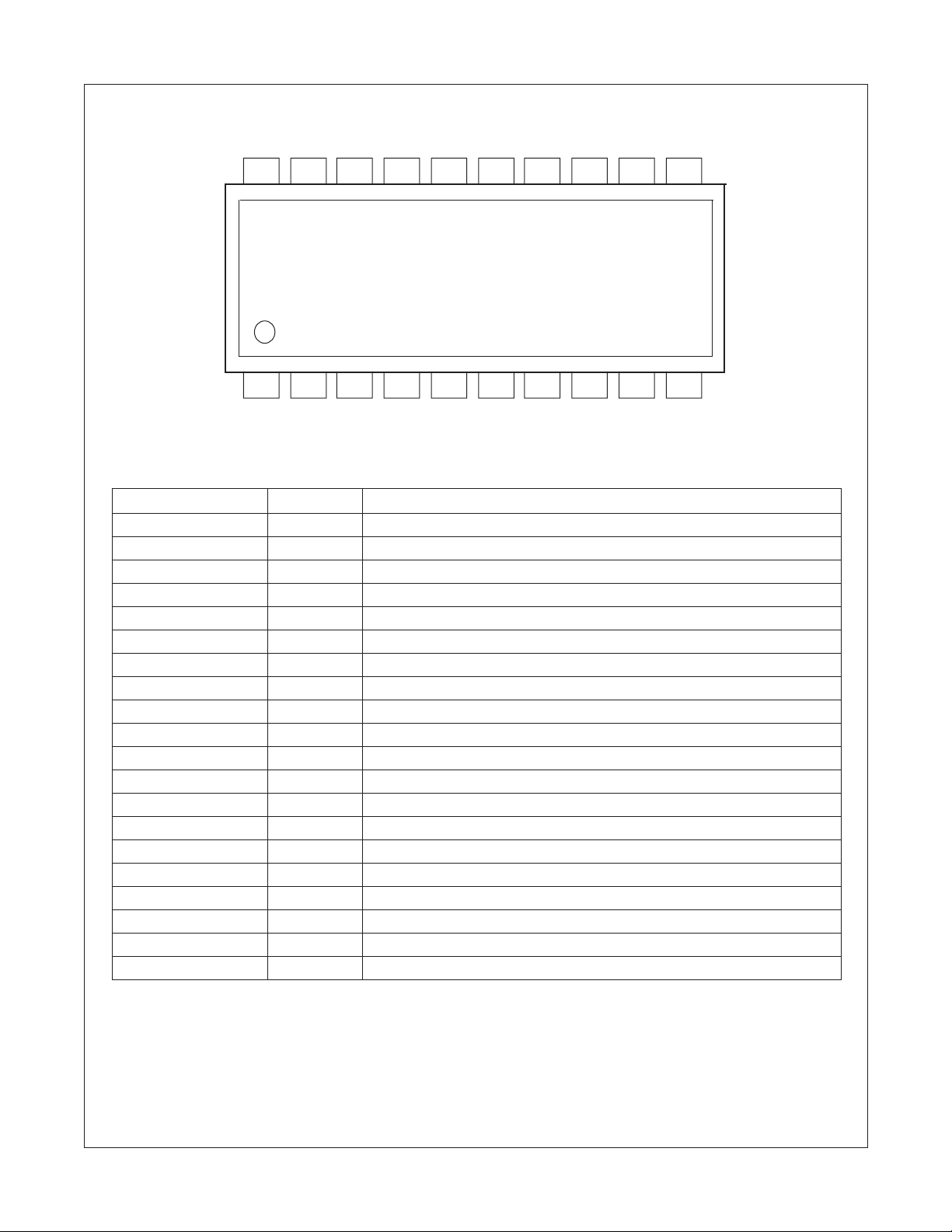
Pin Assignments
FAN7314 LCD Backlight Inverter Drive IC
16
OUTC
15
14
13
RT1 OUTB OUTA VIN PGND OUTD CT RT BCT
20
19
18 17
FAN7314
1
OLP OLR ENA S_S
2
Pin Definitions
Pin Number Pin Name Pin Function Description
1 OLP Open Lamp Protection
2 OLR Open Lamp Regulation
3 ENA Enable Input
4 S_S Soft Start
5 GND Analog Ground
6 REF 2.5V Reference Voltage
7 ADIM Analog Dimming Input
8 BDIM Burst Dimming Input
9 EA_IN Error Amplifier Input
10 EA_OUT Error Amplifier Output
11 BCT Burst Dimming Timing Capacitor
12 RT Timing Resistor
13 CT Timing Capacitor
14 OUTD NMOSFET Drive Output D
15 OUTC PMOSFET Drive Output C
16 PGND Power Ground
17 VIN Supply Voltage
18 OUTA PMOSFET Drive Output A
19 OUTB NMOSFET Drive Output B
20 RT1 Striking Frequency Resistor
543
GND
REF ADIM BDIM EA_IN EA_OUT
12
11
9876
10
FAN7314 Rev. 1.0.1
3
www.fairchildsemi.com
Page 4
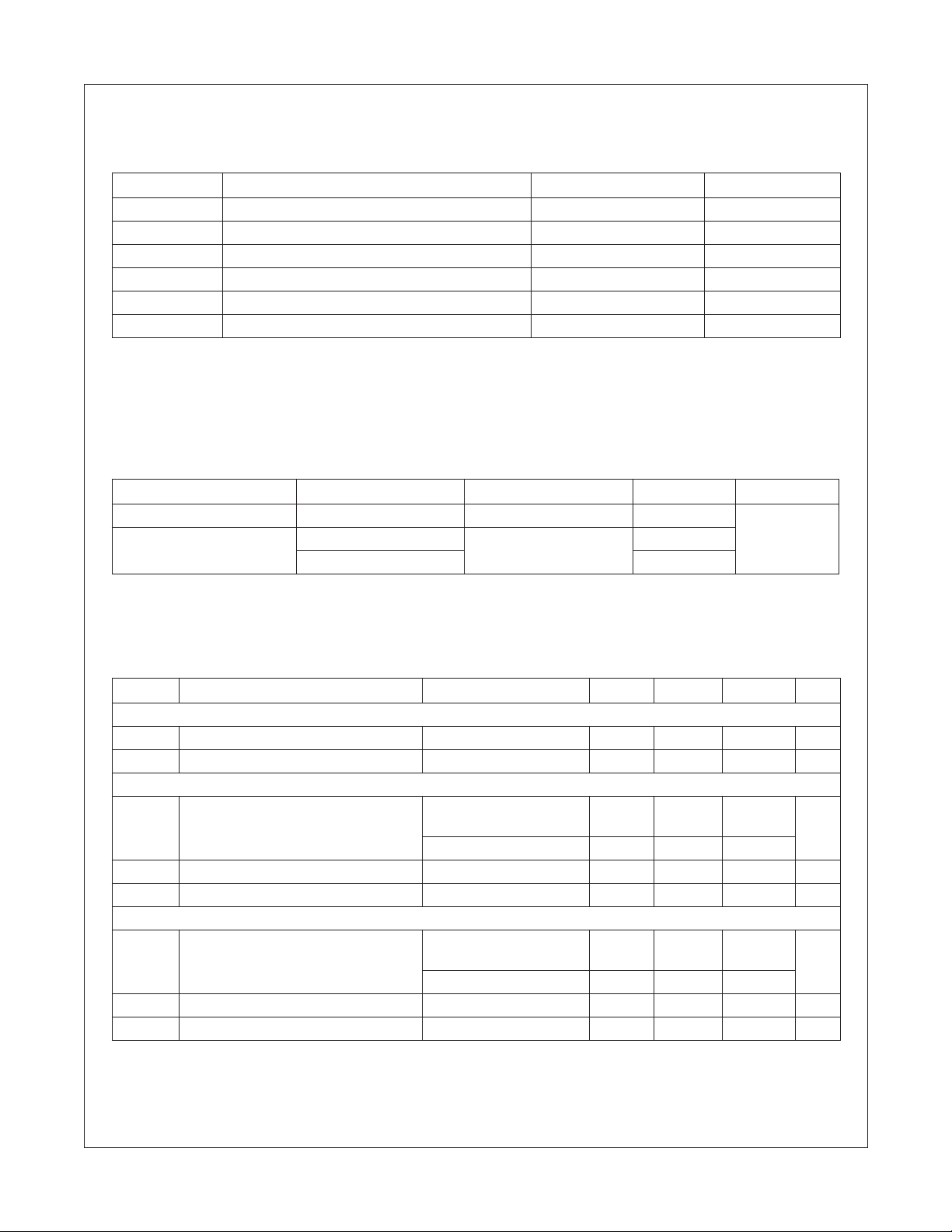
Absolute Maximum Ratings
For typical values T
–25
°
C
≤
T
≤
A
Symbol Parameter Value Unit
V
CC
Topr Operating Temperature Range -25 to 85
Tj Junction Temperature 150
Tstg Storage Temperature Range -65 to 150
R
θ
JA
Pd Power Dissipation 1.8 W
Notes:
1. Thermal resistance test board:
Size: 76.2mm x 114.3mm x 1.6mm(1S0P)
JEDEC standard: JESD51-2, JESD51-3
2. Assume no ambient airflow.
= 25
°
C, V
85
°
C and 5V
A
= 12V and for min/max values T
CC
≤
V
≤
25.5V, unless otherwise specified.
CC
is the operating ambient temperature range with
A
Supply Voltage 5 to 25.5 V
Thermal Resistance Junction-Air
(1, 2)
70
ESD Level
°
°
°
°
C/W
FAN7314 LCD Backlight Inverter Drive IC
C
C
C
Parameter Pins Conditions Level Unit
Human Body Model (HBM) All pins R = 1.5k
Machine Model (MM) All pins except for BDIM C = 200pF 300
BDIM 250
Ω
, C = 100pF 2000 V
Electrical Characteristics
For typical values T
–25
°
C
≤
T
≤
A
Symbol Characteristics Test Condition Min. Typ. Max. Unit
REFERENCE SECTION (Recommend X7R Capacitor)
∆
Vref Line Regulation 5
V25 2.5V Regulation Voltage 2.45 2.5 2.55 V
OSCILLATOR SECTION (Main)
fosc Oscillation Frequency T
Vcth CT High Voltage – 2.0 – V
Vctl CT Low Voltage – 0.5 – V
OSCILLATOR SECTION (Burst)
foscb Oscillation Frequency T
Vbcth BCT High Voltage – 2 – V
Vbctl BCT Low Voltage – 0.5 – V
85
°
C and 5V
= 25
A
°
C, V
= 12V and for min/max values T
CC
≤
V
≤
25.5V, unless otherwise specified.
CC
is the operating ambient temperature range with
A
≤
V
≤
25.5V – 2 25 mV
CC
= 25
°
A
C, Ct = 270pF
110.4 115 119.6 kHz
Rt = 18k
Ct = 270pF, Rt = 18k 108 115 122
= 25
°
A
C, Ctb = 10nF,
204.75 225 245.25 Hz
Rt = 18k
Ctb = 10nF, Rt = 18k 201 225 248
FAN7314 Rev. 1.0.1
4
www.fairchildsemi.com
Page 5
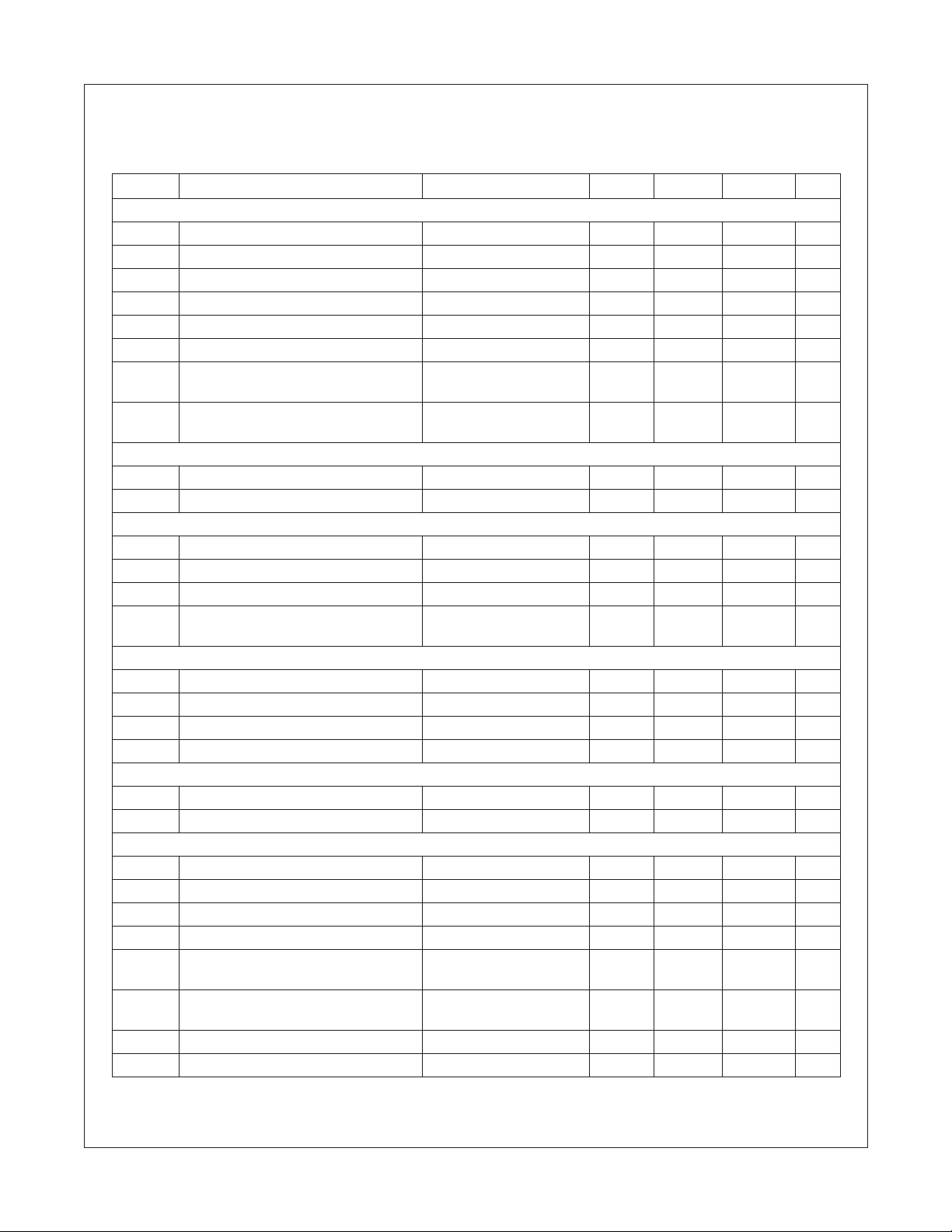
FAN7314 LCD Backlight Inverter Drive IC
Electrical Characteristics
For typical values T
–25
°
C
≤
T
≤
A
85
°
C and 5V
= 25
A
°
C, V
≤
(Continued)
= 12V and for min/max values T
CC
V
≤
25.5V, unless otherwise specified.
CC
is the operating ambient temperature range with
A
Symbol Characteristics Test Condition Min. Typ. Max. Unit
ERROR AMP SECTION
(1)
(1)
(1)
(1)
–80 –dB
– 1.5 – MHz
61 85 109 µA
R(EA_IN) = 60k
→
open lamp 1.3 1.5 1.7 V
0.1 Va
Ω
Va
+
0.4 Va
+
+
0.7 1.4 2.1 µA
= Vth–0.2 – 130 180 µA
CC
= 12V – 1.5 4 mA
CC
= 12V – 200 370 µA
CC
= 12V – Vcc – V
CC
= 12V Vcc–10.5 Vcc–8.5 Vcc–6.5 V
CC
= 12V 6.5 8.5 10.5 V
CC
= 12V – 0 – V
CC
V
= Vth–0.2 Vcc–0.3 – – V
CC
V
= Vth–0.2 – – 0.3 V
CC
V
= 12V, Cload = 2nF – 200 500 ns
CC
V
= 12V, Cload = 2nF – 200 500 ns
CC
0.7 V
Open Loop Gain
Unit Gain Bandwidth
VehFeedback Output High Voltage EA_IN = 0V 2.13 2.4 2.57 V
lsin Output Sink Current EA_OUT = 1.5V – – -1 mA
lsur Output Source Current EA_OUT = 1.5V 1 – – mA
Iolr EA_IN Driving Current On OLR 75 105 135 µA
Iburst EA_IN Driving Current On Burst
Dimming
Vfbh Feedback High Voltage On Burst
Dimming
SOFT START SECTION
I
Soft Start Current S_S = 2V 4 6 8 µA
SS
Vssh Soft Start Clamping Voltage 2.3 2.65 3 V
PROTECTION SECTION
Volp0 Open Lamp Protection Voltage 0 Start at open lamp 2.2 2.5 2.8 V
Volp1 Open Lamp Protection Voltage 1 Normal
Volr Open Lamp Regulation Voltage 1.75 2 2.25 V
Iolp Open Lamp Protection Charging
Current
UNDER VOLTAGE LOCK OUT SECTION
Vth Start Threshold Voltage – – 5 V
Ist Start Up Current V
Iop Operating Supply Current V
Isb Stand-by Current V
ON/OFF SECTION
Von On State Input Voltage 2 – 5 V
Voff Off Stage Input Voltage – – 0.7 V
OUTPUT SECTION
Vpdhv PMOS Gate High Voltage V
Vphlv PMOS Gate Low Voltage V
Vndhv NMOS Gate Drive Voltage V
Vndhv NMOS Gate Drive Voltage V
Vpuv PMOS Gate Voltage With UVLO
Activated
Vnuv NMOS Gate Voltage With UVLO
Activated
Tr Rising Time
Tf Falling Time
FAN7314 Rev. 1.0.1
5
www.fairchildsemi.com
Page 6

Symbol Characteristics Test Condition Min. Typ. Max. Unit
MAX./MIN. OVERLAP
Min. Overlap Between Diagonal
Switches
Max. Overlap Between Diagonal
Switches
(1)
(1)
DELA Y TIME
PDR_A/NDR_B
PDR_C/NDR_D
Notes:
1. These parameters, although guranteed, are not 100% tesed in production.
2. Specifications to -25°C to 85°C are guaranteed by design based on final characterization results.
(1)
(1)
fosc = 100kHz – 0 – %
fosc = 100kHz – 100 – %
Rt = 18k – 450 – ns
Rt = 18k – 450 – ns
FAN7314 LCD Backlight Inverter Drive IC
FAN7314 Rev. 1.0.1
6
www.fairchildsemi.com
Page 7
Function Description
UVLO: The under voltage lockout circuit guarantees
stable operation of the IC’s control circuit by stopping
and starting operation as a function of the Vin value. The
UVLO circuit turns on the control circuit when Vin
exceeds 5V. When Vin is lower than 5V, the IC’s standby
current is less than 200µA.
ENA: Applying voltage higher than 2V to the ENA pin
enables the operation of the IC. Applying voltage lower
than 0.7V to the ENA pin will disable the operation of the
inverter.
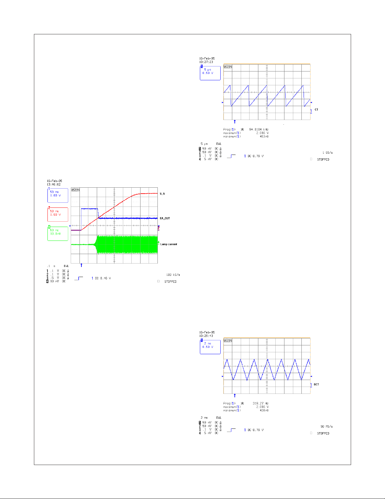
Soft start: The soft start function requires that the S_S
pin is connected through a capacitor to GND. A soft star t
circuit ensures a gradual increase in the input and output
power. The capacitor value connected to the S_S pin
determines the rate at which the duty ratio rises. It is
charged by a 6µA current source.
Burst oscillator & burst dimming: The timing capaci-
tors (BCTs) are charged by the reference current source,
which is formed by the timing resistor (R
). The timing
T
resistor’s voltage is regulated at 1.25V. The sawtooth
waveform charges up to 2V. Once this voltage is
reached, the capacitors begin discharging down to 0.5V.
Next the timing capacitors start charging again and a
new switching cycle begins. The burst dimming frequency can be programmed by adjusting the R
BC
values. The burst dimming frequency can be calcu-
T
and
T
lated as shown below:
FAN7314 LCD Backlight Inverter Drive IC
Main oscillator: The timing capacitors (CTs) are
charged by the reference current source. The current
source is formed by the timing resistor (R
). The timing
T
resistor’s voltage is regulated at 1.25V. The sawtooth
waveform (see top of next column) charges up to 2V.
Once this voltage is reached, the capacitors begin discharging down to 0.5V. Next, the timing capacitors start
charging again and a new switching cycle begins. The
main frequency can be programmed by adjusting the R
and CT values. The main frequency can be calculated as
shown below:
19
-------------------------------
fop =
32 RT C
T
f
burst
3.75
=
----------------------------------96 RT BC
T
To avoid visible flicker, the burst dimming frequency
should be greater than 120Hz.
By comparing the input of BDIM pin with the 0.5 to 2V
triangular wave of the burst oscillator, the PWM pulses
for burst dimming. The PWM pulse controls EA_OUT’s
voltage by summing 85µA into the EA_IN pin.
T
FAN7314 Rev. 1.0.1
7 www.fairchildsemi.com
Page 8
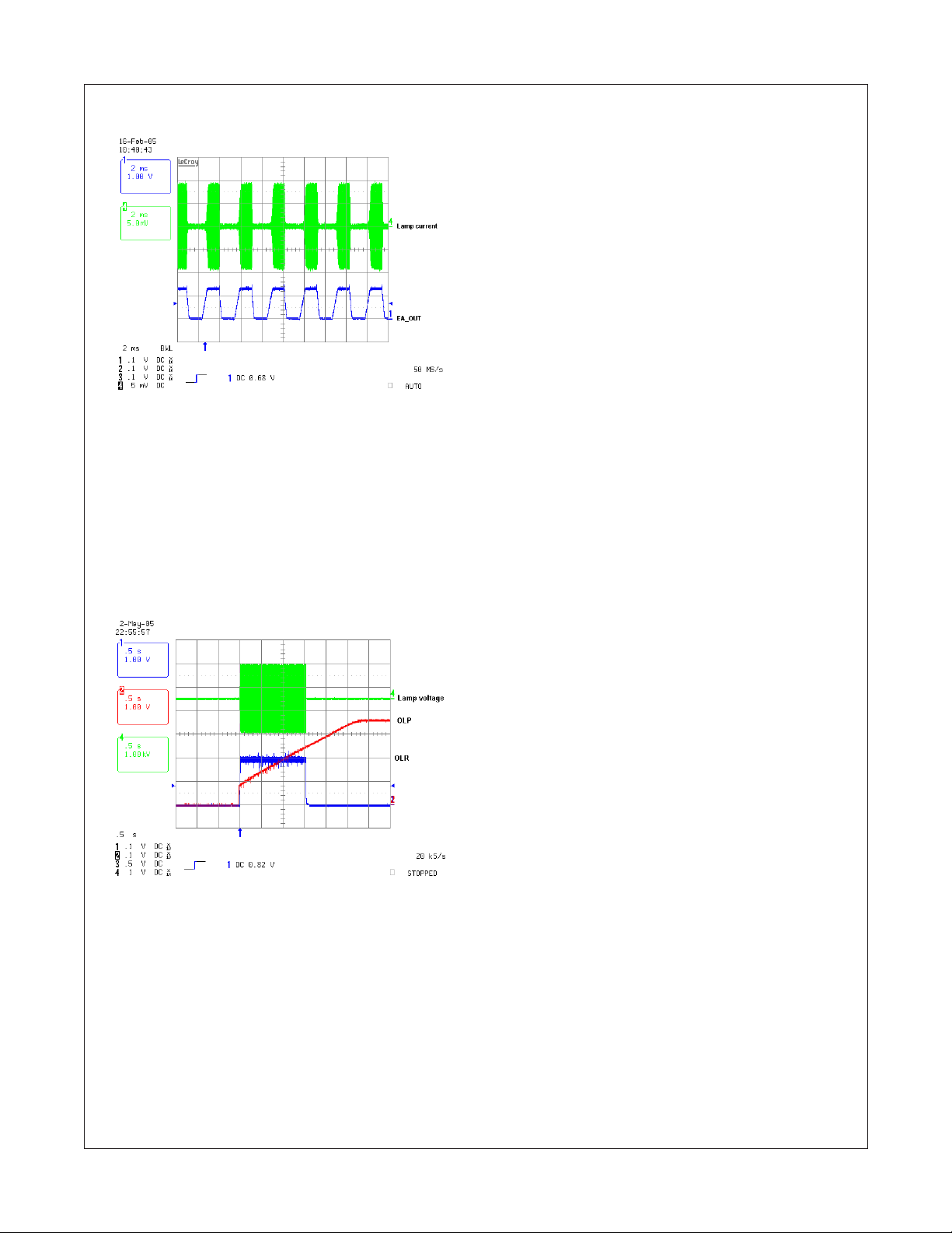
Open lamp regulation & open lamp protection: It is
necessary to suspend power stage operation if an open
lamp occurs, because the power stage has high gain.
When a voltage higher than 2V is applied to the OLR pin,
the part enters regulation mode and controls the
EA_OUT voltage. This limits the lamp voltage by summing 105µA into the feedback node. At the same time,
the OLP capacitor, connected to the OLP pin, is charged
by the 1.4µA internal current source. Once it reaches
2.5V, the IC enters shut down where all the output is
high.
FAN7314 LCD Backlight Inverter Drive IC
Output Drives: The four output drives are designed so
that switches A and B, C and D never turn on simultaneously. The OUTA-OUTB pair is intended to drive one
half-bridge in the external power stage. The OUTCOUTD pair will drive the other half-bridge.
FAN7314 Rev. 1.0.1
8 www.fairchildsemi.com
Page 9
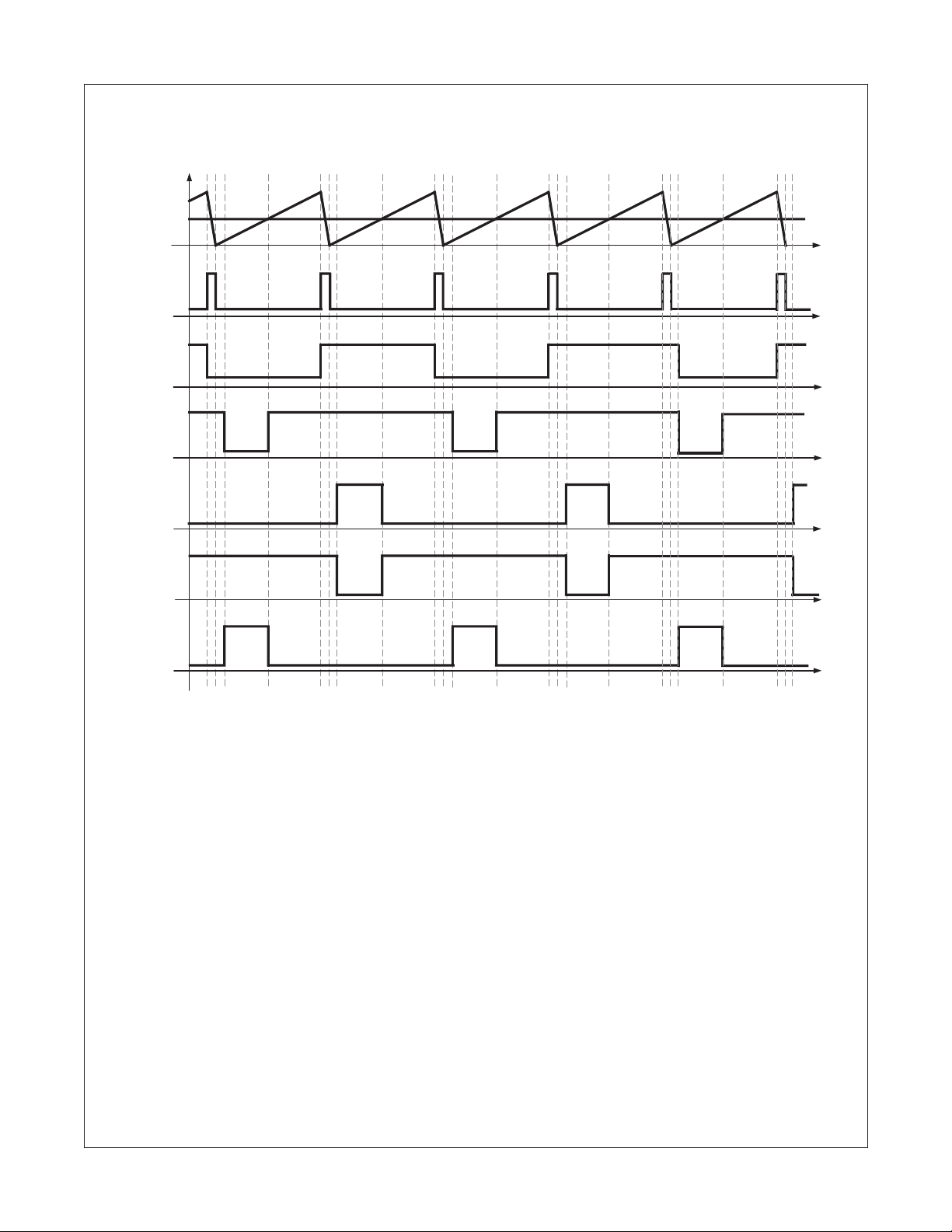
Timing Diagram
The FAN7314 uses the half-bridge to drive CCFL.
EA_OUT
CT
SYNC
T
POUT A
NOUT B
FAN7314 LCD Backlight Inverter Drive IC
POUT C
NOUT D
FAN7314 Rev. 1.0.1
9 www.fairchildsemi.com
Page 10
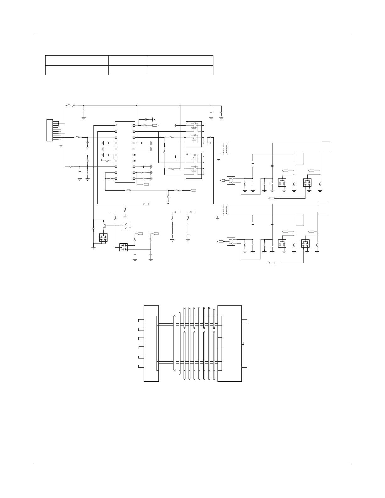
Typical Application Circuit
Application Lamps Input Volta ge
19 inch LCD Monitor 4 13V
1. Schematic
F1
FUSE
ON/OFF
R4
22k
C22
220u
25V
0
R24
10k
C28
10n
0
REF
R2
56k
C21
R3
18k
10n
0
0
IC1 FAN7314
OLP
OLR
ENA
C1 0.22u
S_S
0
GND
0
C2 1u
0
REF
ADIM
R7 0
BDIM
EA_IN
C3
EA_OUT
4.7n
REF
R1
OLP
330k
C9
Q1
1u
KST2222
D1
BAW56
0
C260.1u
0
R6 82k
PGND
OUTC
OUTD
R8
100k
R14
100k
RT1
OUTB
OUTA
VIN
CT
RT
BCT
C6
1u
C5 220p
R5 27k
C4
4.7n
OUTB
OUTA
RT
0
0
J1
0
0
0
0
RT
OLR
0
D11
BAW56
OLP3 OLP4
R21
R20
10k
10k
D10
BAW56
C18
C17
2.2n
2.2n
0
0
CN5
12505WR-10
1
13V
2
3
4
5
6
7
8
9
10
0
DIM ( 0~3.3V)
FAN7314 LCD Backlight Inverter Drive IC
C25
C27
1u
1u
M1
0
SN
GN
R25
SP
10k
GP
FDS8958A
M2
0
SN
GN
R27
SP
10k
GP
FDS8958A
R15
10k
R9
9.1k
0
R22
R23
10k
10k
C19
C20
2.2n
2.2n
00
0
0
DN
DN
C7 10u
DP
DP
DN
DN
DP
DP
FB
C8 10u
TX1
0
OLR
D4
BAV70
R26
1k
0 0
TX2
OLP2OLP1
0
OLR
D3
BAV70
R12
1k
0 0
LTM190EX
1
HOT
CN2
CCFL
2
C10
15p
C14
10n
0 0
C11
15p
OLP1
C30
R13
10n
1k
0
FB
C12
15p
C29
10n
0
C13
15p
OLP3 OLP4
R11
C15
1k
10n
0
COLD
OLP2
D6
BAV99
0
D8
BAV99
0
D7
BAV99
R17
1k
0
0
1
1
HOT
2
COLD
R18
1k
0
2
CN4
CCFL
D9
BAV99
0
1
HOT
CN1
CCFL
2
COLD
R16
1k
HOT
CN3
CCFL
COLD
R19
1k
0
FB
2. Transformer Schematic Diagram
Supported by Namyang electronics (http://www.namyangelec.co.kr)
1
6
9
8
234567
3. Core & Bobbin
■ Core: EFD2124
■ Material: PL7
■ Bobbin: EFE2124
9
7
1
FAN7314 Rev. 1.0.1
10 www.fairchildsemi.com
Page 11
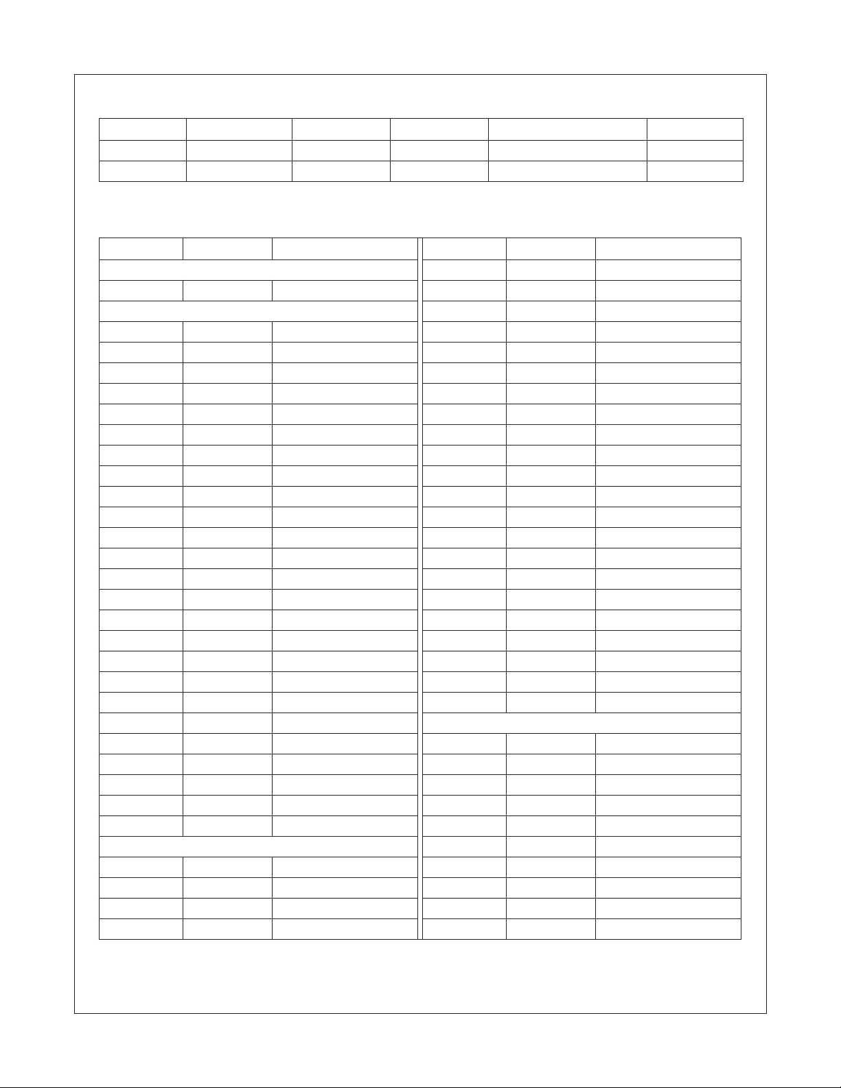
4. Winding Specification
Pin No. Wire Turns Inductance Leakage Inductance Remarks
5 → 2 1 UEW 0.45 φ 12 180µH 7.2µH 1KHz, 1V
7 → 9 1 UEW 0.04 φ 2430 (270 x 9) 7.2H 330mH 1KHz, 1V
5. BOM of the Application Circuit
Part Ref. Value Description/Vendor Part Ref. Value Description/Vendor
Fuse C5 220p 50V 1608 J
F1 24V 3A Fuse C6 1µ 50V 2012 K
Resistor (SMD) C7 10µ 16V 3216
R1 330K 1608 J C8 10µ 16V 3216
R2 56K 1608 F C9 1µ 16V 1608 K
R3 18K 1608 F C10 15p 3KV 3216
R4 22K 1608 F C11 15p 3KV 3216
R5 27K 1608 F C12 15p 3KV 3216
R6 82K 1608 F C13 15p 3KV 3216
R8 100K 1608 F C14 10n 50V 1608 K
R9 9.1K 1608 F C15 10n 50V 1608 K
R11 1K 1608 F C17 2.2n 50V 1608 Z
R12 1K 1608 F C18 2.2n 50V 1608 Z
R13 1K 1608 F C19 2.2n 50V 1608 Z
R14 100K 1608 F C20 2.2n 50V 1608 Z
R15 10K 1608 F C21 10n 50V 1608 Z
R16 1K 1608 F C25 1µ 50V 2012 K
R17 1K 1608 F C26 0.1µ 16V 1608 K
R18 1K 1608 F C27 1µ 50V 2012 K
R19 1K 1608 F C28 10n 50V 1608 Z
R20 10K 1608 J C29 10n 50V 1608 K
R21 10K 1608 J C30 10n 50V 1608 K
R22 10K 1608 J Diode / TR (SMD)
R23 10K 1608 J D1 BAW56 Fairchildsemi
R24 10K 1608 J D3 BAV70 Fairchildsemi
R25 10K 1608 J D4 BAV70 Fairchildsemi
R26 1K 1608 F D6 BAV99 Fairchildsemi
R27 10K 1608 J D7 BAV99 Fairchildsemi
Capacitor (SMD) D8 BAV99 Fairchildsemi
C1 0.22µ 16V 1608 K D9 BAV99 Fairchildsemi
C2 1µ 50V 2012 K D10 BAW56 Fairchildsemi
C3 4.7n 50V 1608 K D11 BAW56 Fairchildsemi
C4 4.7n 50V 1608 K Q1 KST2222 Fairchildsemi
FAN7314 LCD Backlight Inverter Drive IC
FAN7314 Rev. 1.0.1
11 www.fairchildsemi.com
Page 12
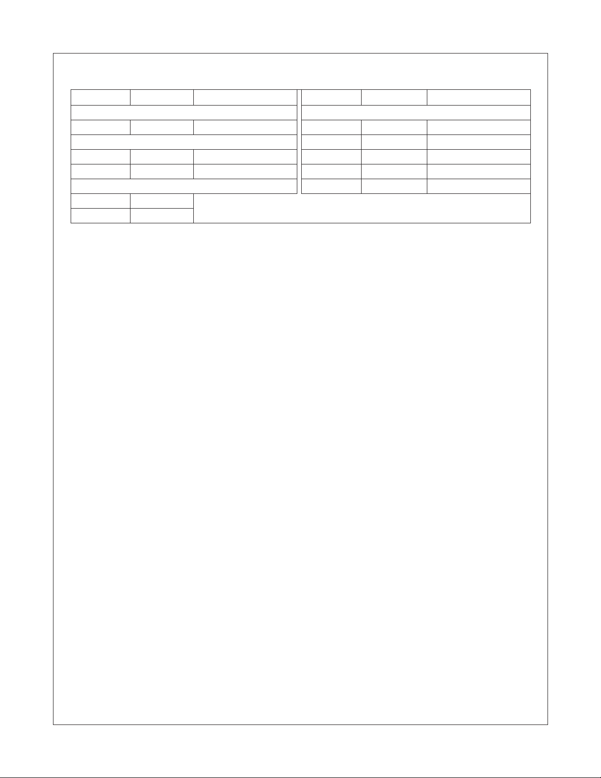
5. BOM of the Application Circuit (Continued)
Part Ref. Value Description/Vendor Part Ref. Value Description/Vendor
Electrolytic capacitor Wafer (SMD)
C22 220µ 25V CN1 35001WR-02A
MOSFET (SMD) CN2 35001WR-02A
M1 FDS8958A Fairchildsemi CN3 35001WR-02A
M2 FDS8958A Fairchildsemi CN4 35001WR-02A
Transformer (SMD) CN5 12505WR-10
TX1 EFD2124 Supported by Namyang electronics
TX2 EFD2124
(http://www.namyangelec.co.kr)
FAN7314 LCD Backlight Inverter Drive IC
FAN7314 Rev. 1.0.1
12 www.fairchildsemi.com
Page 13

Mechanical Dimensions
20-pin SOIC Package
FAN7314 LCD Backlight Inverter Drive IC
20
11
Symbol
A .093 .104 2.35 2.65
A1 .004 .012 0.10 0.30
B .013 0.33
C .009 .013 0.23 0.32
D .496 .512 12.60 13.00
E .291 .299 7.40 7.60
e
H
h
L .016 .050 0.40 1.27
N20 20
α
ccc .004 0.10——
Notes:
1.
Dimensioning and tolerancing per ANSI Y14.5M-1982.
2.
"D" and "E" do not include mold flash. Mold flash or
protrusions shall not exceed .010 inch (0.25mm).
3.
"L" is the length of terminal for soldering to a substrate.
4.
Terminal numbers are shown for reference only.
5.
"C" dimension does not include solder finish thickness.
6.
Symbol "N" is the maximum number of terminals.
Inches
Min. Max. Min. Max.
.020 0.51
.050 BSC 1.27 BSC
.394 .419 10.00 10.65
.010 .029 0.25 0.75
0° 8° 0° 8°
Millimeters
Notes
5
2
2
3
6
1
A
e
FAN7314 Rev. 1.0.1
EH
10
D
A1
B
SEATING
PLANE
– C –
LEAD COPLANARITY
ccc C
13 www.fairchildsemi.com
α
h x 45°
C
L
Page 14
TRADEMARKS
The following are registered and unregistered trademarks Fairchild Semiconductor owns or is authorized to use and is
not intended to be an exhaustive list of all such trademarks.
ACEx™
ActiveArray™
Bottomless™
FPS™
Build it Now™
CoolFET™
CROSSVOLT™
DOME™
EcoSPARK™
2
E
CMOS™
EnSigna™
FACT™
FACT Quiet Series™
Across the board. Around the world.™
The Power Franchise
Programmable Active Droop™
DISCLAIMER
FAIRCHILD SEMICONDUCTOR RESERVES THE RIGHT TO MAKE CHANGES WITHOUT FURTHER NOTICE TO ANY
PRODUCTS HEREIN TO IMPROVE RELIABILITY, FUNCTION OR DESIGN. FAIRCHILD DOES NOT ASSUME ANY LIABILITY
ARISING OUT OF THE APPLICATION OR USE OF ANY PRODUCT OR CIRCUIT DESCRIBED HEREIN; NEITHER DOES IT
CONVEY ANY LICENSE UNDER ITS PATENT RIGHTS, NOR THE RIGHTS OF OTHERS.
LIFE SUPPORT POLICY
®
FAST
FASTr™
LittleFET™
FRFET™
GlobalOptoisolator™
GTO™
HiSeC™
2
I
C™
i-Lo™
ImpliedDisconnect™
IntelliMAX™
®
ISOPLANAR™
MICROCOUPLER™
MicroFET™
MicroPak™
MICROWIRE™
MSX™
MSXPro™
OCX™
OCXPro™
OPTOLOGIC
®
OPTOPLANAR™
PACMAN™
POP™
Power247™
PowerEdge™
PowerSaver™
PowerTrench
®
QFET
®
QS™
QT Optoelectronics™
Quiet Series™
RapidConfigure™
RapidConnect™
µSerDes™
ScalarPump™
SILENT SWITCHER
SMART START™
SPM™
Stealth™
SuperFET™
SuperSOT™-3
SuperSOT™-6
SuperSOT™-8
SyncFET™
TCM™
TinyLogic
TINYOPTO™
TruTranslation™
UHC™
UltraFET
UniFET™
®
VCX™
Wire™
®
®
FAN7314 LCD Backlight Inverter Drive IC
FAIRCHILDíS PRODUCTS ARE NOT AUTHORIZED FOR USE AS CRITICAL COMPONENTS IN LIFE SUPPORT
DEVICES OR SYSTEMS WITHOUT THE EXPRESS WRITTEN APPROVAL OF FAIRCHILD SEMICONDUCTOR CORPORATION.
As used herein:
1. Life support devices or systems are devices or
systems which, (a) are intended for surgical implant into
the body, or (b) support or sustain life, or (c) whose
failure to perform when properly used in accordance
with instructions for use provided in the labeling, can be
reasonably expected to result in significant injury to the
user.
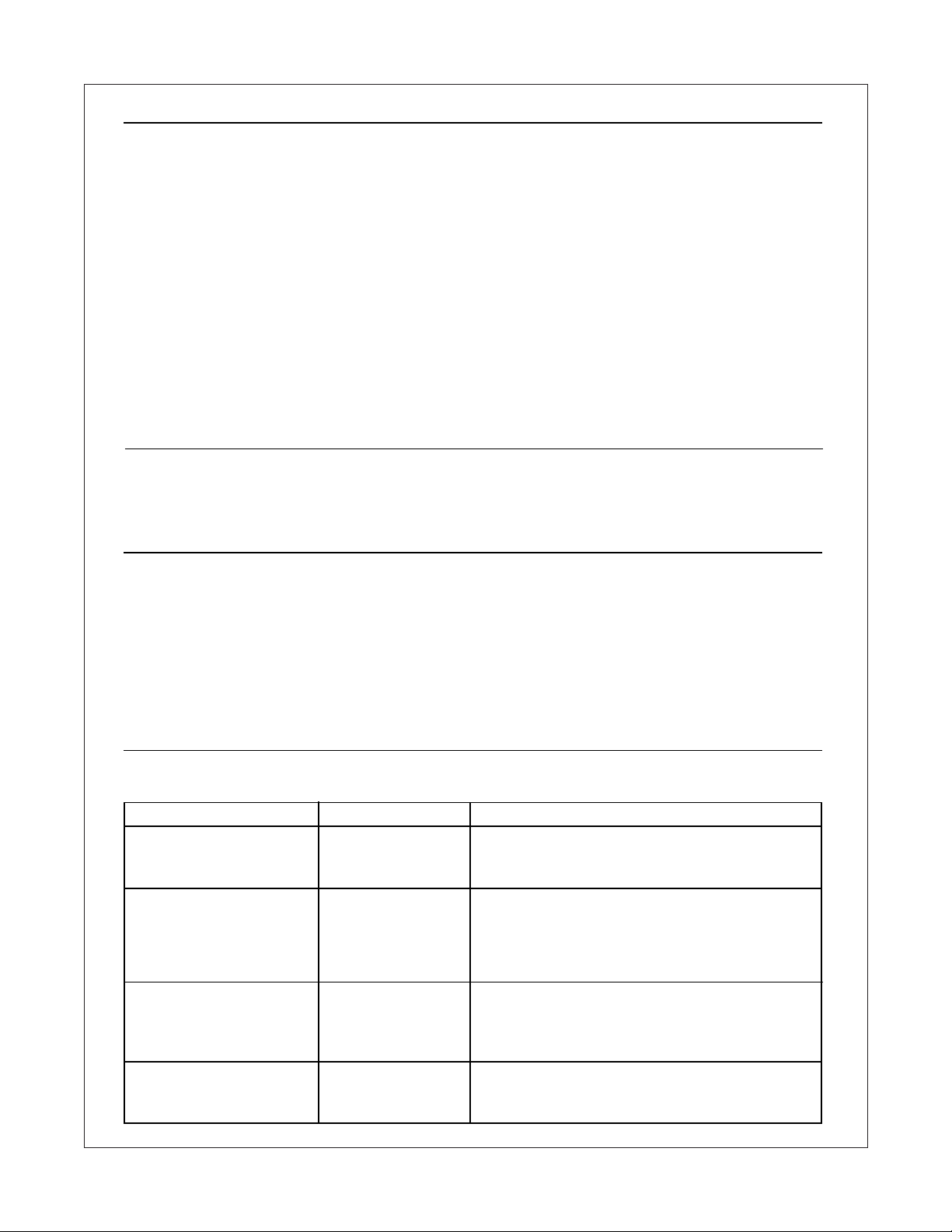
PRODUCT STATUS DEFINITIONS
Definition of Terms
Datasheet Identification Product Status Definition
Advance Information
Preliminary
No Identification Needed
Formative or
In Design
First Production
Full Production
2. A critical component is any component of a life
support device or system whose failure to perform can
be reasonably expected to cause the failure of the life
support device or system, or to affect its safety or
effectiveness.
This datasheet contains the design specifications for
product development. Specifications may change in
any manner without notice.
This datasheet contains preliminary data, and
supplementary data will be published at a later date.
Fairchild Semiconductor reserves the right to make
changes at any time without notice in order to improve
design.
This datasheet contains final specifications. Fairchild
Semiconductor reserves the right to make changes at
any time without notice in order to improve design.
Obsolete
FAN7314 Rev. 1.0.1
Not In Production
This datasheet contains specifications on a product
that has been discontinued by Fairchild semiconductor.
The datasheet is printed for reference information only.
Rev. I18
14 www.fairchildsemi.com
 Loading...